
®
Integrated Circuits Group
ID242 Series
Flash Memory Card
(Model Numbers: ID242xxx)
Spec No.: CPS0002-002
Issue Date: May, 1998
Product Overview
SHARP
ID242 SERIES PRODUCT OVERVIEW
l
Handle this document carefully for it contains material protected by international copyright law. Any reproduction, full or in part, of this material is prohibited without the express written permission of the company.
l
When using the products covered herein, please observe the conditions written herein and the precautions
outlined in the following paragraphs. In no event shall the company be liable for any damages resulting from
failure to strictly adhere to these conditions and precautions.
(1) The products covered herein are designed and manufactured for the following application areas. When
using the products covered herein for the equipment listed in Paragraph (2). even for the following
application areas, be sure to observe the precautions given in Paragraph (2). Never use the products for
the equipment listed in Paragraph (3).
* Office electronics
* Instrumentation and measuring equipment
* Machine tools
* Audiovisual equipment
* Home appliances
* Communication equipment other than for trunk lines
(2) Those contemplating using the products covered herein for the following equipment which demands
high reliability, should first contact a sales representative of the company and then accept responsibility for incorporating into the design fail-safe operation, redundancy, and other appropriate measures for
ensuring reliability and safety of the equipment and the overall system.
* Control and safety devices for airplanes, trains, automobiles, and other transportation equipment
* Mainframe computers
* Traffic control systems
* Gas leak detectors and automatic cutoff devices
* Rescue and security equipment
* Other safety devices and safety equipment, etc.
(3) Do not use the products covered herein for the following equipment which demands extremely high
performance in terms of functionality, reliability, or accuracy.
* Aerospace equipment
* Communications equipment for trunk lines
* Control equipment for the nuclear power industry
* Medical equipment related to life support, etc.
(4) Please direct all queries and comments regarding the interpretation of the above three Paragraphs to a
sales representative of the company.
CPSOOOZ-002 8 May.
SHARI=
ID242 SERIES PRODUCT OVERVIEW
1.
2.
3.
4.
5.
6.
7.
8.
9.
10.
11.
Contents
Introduction.. ...............................................................................................................
P.
Features
.......................................................................................................................
P.
Block Diagram
............................................................................................................
P.
Pin Connections
........... ...............................................................................................
P.
Signal Description
......................................................................................................
P.
Functions.. ...................................................................................................................
P.
6.
1 Common Memory.. .........................................................................................
P.
6.
2 Attribute Memory ...........................................................................................
P.
6. 3 Function Table
................................................................................................
P.
Card Information Structure (CIS)
...............................................................................
P.
Card Control
...............................................................................................................
P.
8. 1 Reset
.............................................................................................................
P.
8. 2 Status Register
................................................................................................
P.
8.
3 Write Protect Switch.. .....................................................................................
P.
8. 4 Identifier Codes..
........ . . ...................................................................................
P.
Component
Management Register
(CMR)
.................................................................
P.
Command Definitions..
...............................................................................................
P.
Electrical Specifications
.............................................................................................
P‘
11. 1 Absolute Maximum Ratings
...........................................................................
P.
11. 2 Recommended Operating Conditions..
...........................................................
P.
11. 3 Capacitance
.....................................................................................................
P.
11. 4 AC Input/Output Test Conditions
..................................................................
P.
12. DC Characteristics
......................................................................................................
P.
13. AC Characteristics
......................................................................................................
P.
13. 1 Common Memory Read Operations..
.............................................................
P.
13. 2 Command Write Operations :
Common Memory..
........................................ P.
13. 3 Attribute Memory Read Operations
...............................................................
P.
13. 4 Attribute Memory Write Operations
..............................................................
P.
13. 5 Power-Up/Power Down
..................................................................................
P.
14. Specification Changes ................................................................................................
P.
15. Other Precautions..
......................................................................................................
P.
16. External
Diagrams ......................................................................................................
P.
3
3
4
5
6
7
7
8
9
9
12
12
12
12
12
14
16
17
17
17
17
17
18
20
20
22
28
29
30
31
31
32
SHARI=
ID242 SERIES PRODUCT OVERVIEW
3
-
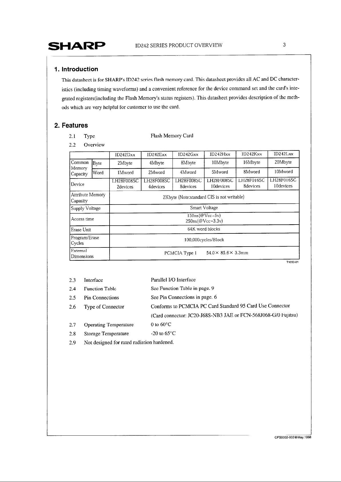
1. Introduction
This datasheet is for SHARP’s ID242 series flash memory card. This datasheet provides all AC and DC characteristics (including timing waveforms) and a convenient reference for the device command set and the card’s inte-
grated registers(including the Flash Memory’s status registers). This datasheet provides description of the meth-
ods which are very helpful for customer to use the card.
2. Features
2.1
Type
Flash Memory Card
2.2
Overview
Erase Unit
Program/Erase
Cycles
External
Dimensions
250ns(@Vcc=3.3v)
64K word blocks
100,000cycles/Block
PCMCIA Type 1
54.0X 85.6X 3.3mm
TlOSO-01
2.3
Interface
Parallel I/O Interface
2.4
Function Table
See Function Table in page. 9
2.5
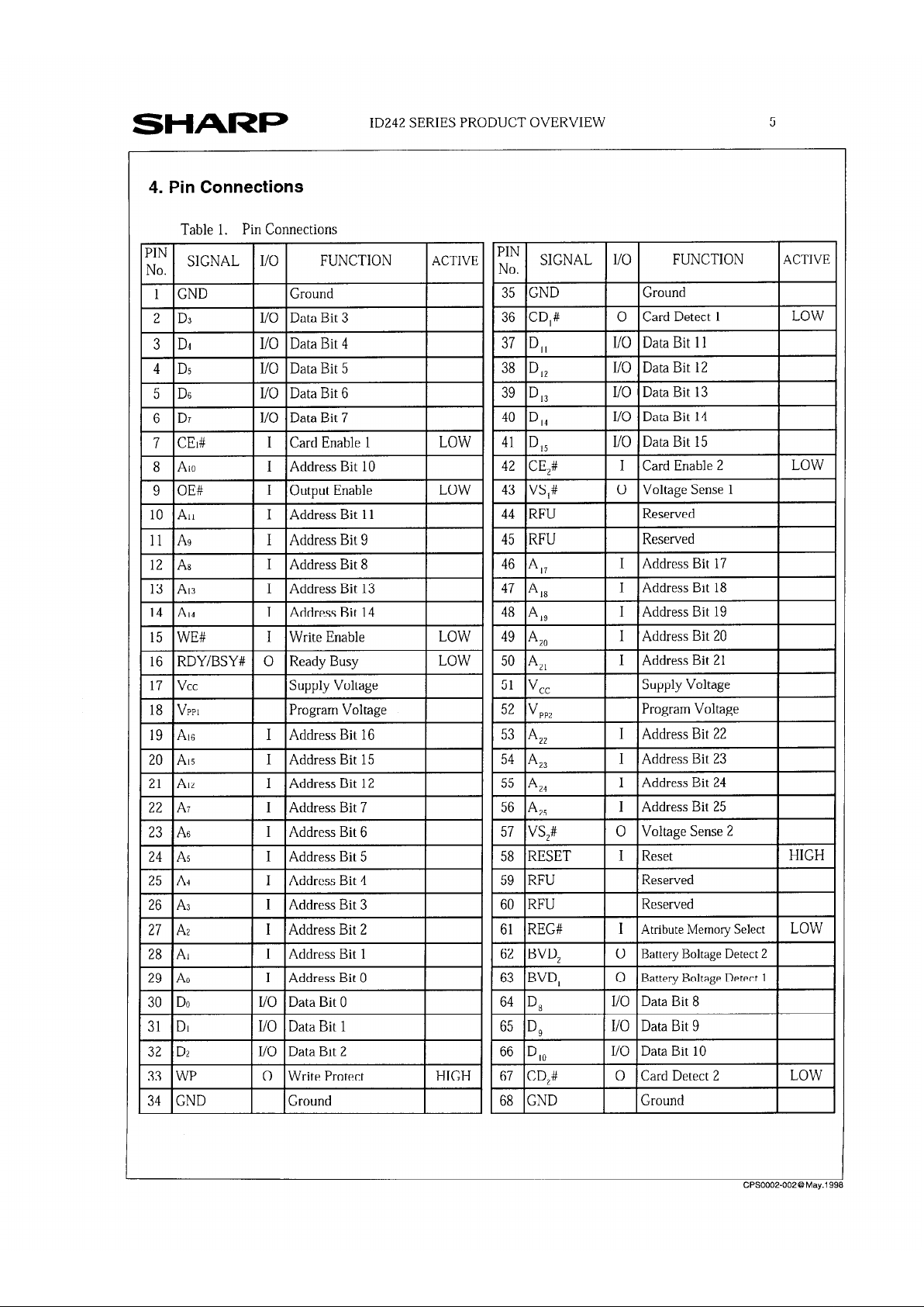
Pin Connections See Pin Connections in page. 6
2.6
Type of Connector
Conforms to PCMCIA PC Card Standard 95 Card Use Connector
(Card connector: JC20-J68S-NB3 JAE or FCN-568J068-G/O Fujitsu)
2.7
Operating Temperature
0 to 60°C
2.8
Storage Temperature
-20
to 65°C
2.9
Not designed for rated radiation hardened.
-
CPS0002.002BMay,19!
SHARP
ID242 SERIES PRODUCT OVERVIEW
4
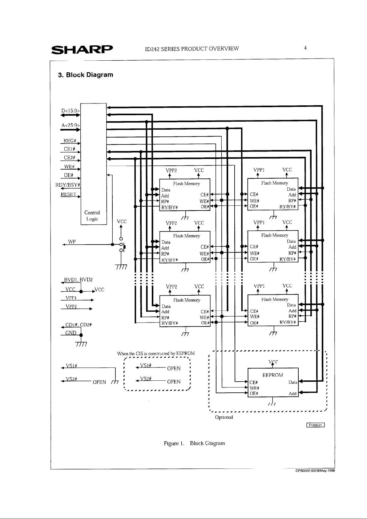
3. Block Diagram
,r
D<15:0>
A<25:0>
REG#
CEl# ,
CE2#
1
1
WE# ,
OE#
RDpSYk
RESET,
: ’
WP
A+
Control
Logic
VPPX vcc
II,t t’
cl
Flash Memory
Data
Add
CE#
I t4
RP#
WE#
RY/RY#
OE#
T
II, t
VPP2
vcc
VPPl vcc
t
t
Flash Memory
Data *I
* CE#
Add ++ WE# RP# -+ OE#
RYrBY# --(
VPPl vcc
t t
Flash Memory
Data c =
+ CE#
Add + + WE# RP# -+ OE#
RYiBY# +’
.
II. I
, I : I
i iI i
=rLc
VPPl
b
VPP2
b
vpp1 vcc
VPP2
vcc
I I I
I
t
:lash Memory
Data 4
Add + - 4
RP# --
RY/BY# -
I
I I
I
RY/BY#
OE#
I I
__*1 OE#
EEPROM
- CE# Data M
b WE#
- OE#
Add v
. CDl#, CDL%
I
I
I
I
*
I
I
I
,
I
*
I
9
I
I
,
I
I
I
I
I
I
I
I
I
I
I
I
I
Figure 1. Block Giagrarn
SHARI=
ID242 SERIES PRODUCT OVERVIEW
5
4. Pin Connections
Table 1. Pin Connections
;,” SIGNAL I/O FUNCTION
ACTIVE
LOW
HIGH
1 35 IGND
1 IGround
1 39 ID,,
I I/O I Data Bit 13
I
43 IVS,#
I I
0 Voltage Sense 1
I 44 IRFU 1 1 Reserved
1 1 Reserved
I I 1 Address Bit 17
I 45 IRFU
1 46 IA,,
54 43
55 A74
I Address Bit 23
I Address Bit 24
1 56 IA,,
I I 1 Address Bit 25
1 I I Reset
0 Voltage Sense 2
I 58 IRESET
57 VS,#
I
62 IBVD,
I
0 Battery Boltage Detect 2
63 BVD, 0
Battery Boltage Detect 1
Data Bit 8 64
DR
I/O
65
DQ
I/O Data Bit 9
66 I/O
Data Bit 10
D,Ll
67 CD,#
I -
68 IGND
0 Card Detect 2
1 Ground
CPSOOO2-002 @ May.1 998
SHARP
ID242 SERIES PRODUCT OVERVIEW
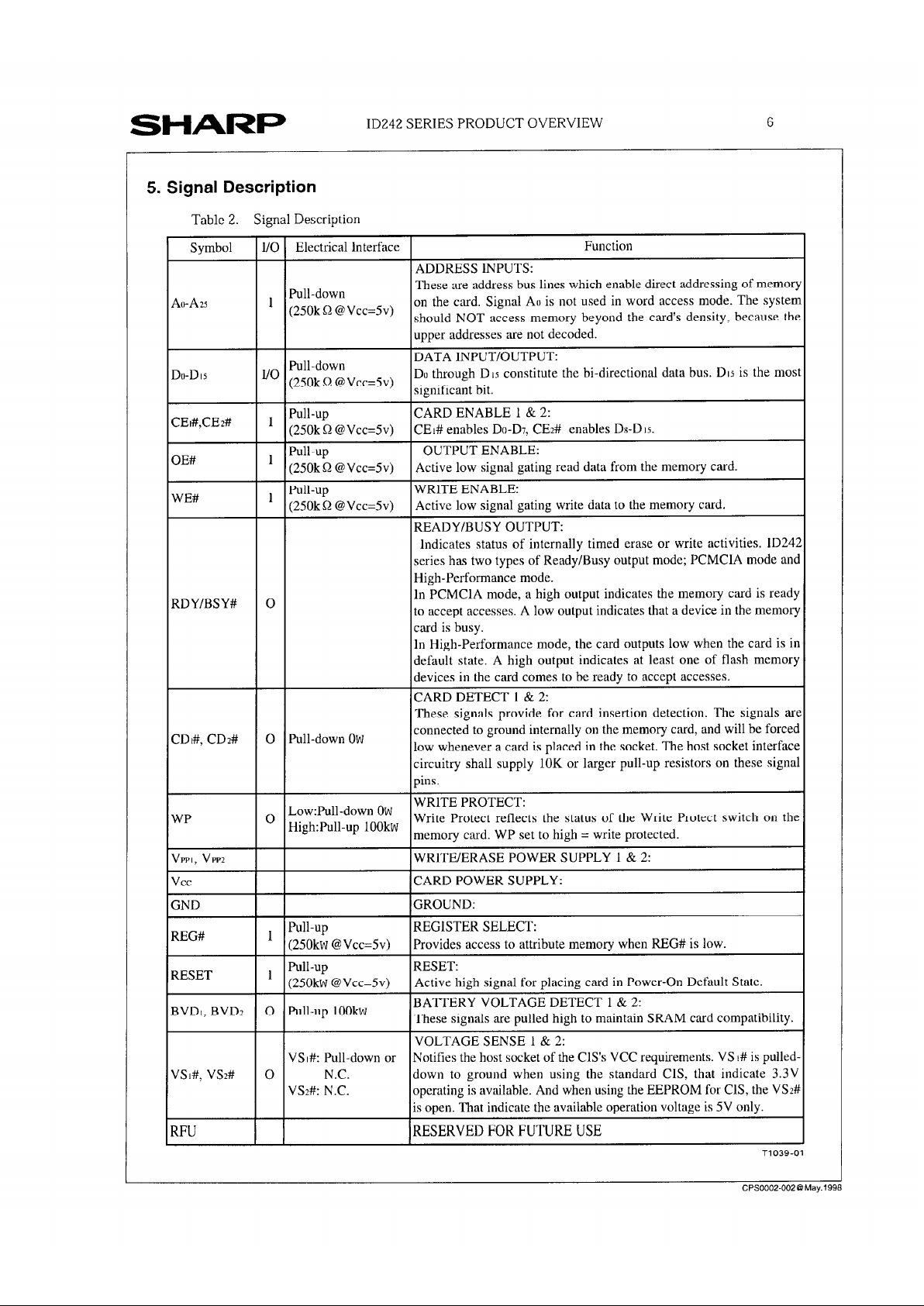
5. Signal Description
Table 2. Signal Description
Symbol l/O Electrical interface
Function
ADDRESS INPUTS:
Ao-Azs
Du-D15
1 Pull-down
These are address bus lines which enable direct addressing of memory
(250k Q @ Vcc=Sv)
on the card. Signal AI) is not used in word access mode. The system
should NOT access memory beyond the card’s density. because the
upper addresses are not decoded.
DATA INPUT/OUTPUT:
1/o Pull-down
(2’0k ’ @VCC=‘V)
De through Dls constitute the bi-directional data bus. DIG is the most
significant bit,
CEI#,CEZ#
OE#
WE#
1 Pull-up CARD ENABLE I & 2:
(250k Q @Vcc=Sv)
CEI# enables Do-D7, CE2# enables Dx-DIG.
1 Pull-up OUTPUT ENABLE:
(250k Q @ Vcc=Sv)
Active low signal gating read data from the memory card.
1 Pull-up WRlTE ENABLE:
(250k 52 @ Vcc=Sv) Active low signal gating write data to the memory c‘ard.
READY/BUSY OUTPUT:
indicates status of internally timed erase or write activities. lD242
series has two types of Ready/Busy output mode; PCMClA mode and
High-Performance mode.
RDY/BSY# 0
In PCMClA mode, a high output indicates the memory card is ready
to accept accesses. A low output indicates that a device in the memory
c,ard is busy.
In High-Performance mode, the card outputs low when the card is in
default state. A high output indicates at least one of flash memory
devices in the card comes to be ready to accept accesses.
CARD DETECT 1 & 2:
These signals provide for card insertion detection. The signals are
CDt#, CD2# 0 Pull-down Ow
connected to ground internally on the memory card, and will be forced
low whenever a card is placed in the socket. The host socket interface
circuitry shall supply 10K or larger pull-up resistors on these signal
pins.
o LowPull-down OW
WRlTE PROTECT:
WP
High:Pull-up 1OOkw
Write Protect reflects the status of the Write Protect switch on the
memory card. WP set to high = write protected.
VPPI,
VW2
WRITE/ERASE POWER SUPPLY 1 & 2:
vcc CARD POWER SUPPLY:
GND GROUND:
REG#
1 Pull-up
REGlSTER SELECT:
(250kw @Vcc=Sv) Provides access to attribute memory when REG# is low.
RESET
1 Pull-up RESET:
(250kw @Vcc=Sv)
Active high signal for placing card in Power-On Default State.
BVDt, BVD2 0 Pull-up 1OOkw
BATTERY VOLTAGE DETECT 1 & 2:
These signals are pulled high to maintain SRAM card compatibility.
VOLTAGE SENSE 1 & 2:
VSI#: Pull-down or Notifies the host socket of the ClS’s
VCC
requirements. VS I# is pulled-
VSI#,
VS2#
0 N.C. down to ground when using the standard ClS, that indicate 3.3V
VSB: N.C. operating is available. And when using the EEPROM for ClS, the VS2#
is open. That indicate the available operation voltage is 5V only.
RFU
RESERVED FOR FUTURE USE
CPSOOOZ-002@Mav.1991
SHARP
ID242 SERIES PRODUCT OVERVIEW 7
6. Functions
6.1 Common Memory
6. 1. 1 Common Memory Architecture
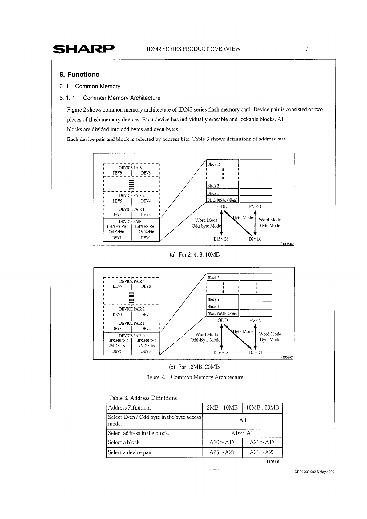
Figure 2 shows common memory architecture of ID242 series flash memory card. Device pair is consisted of two
pieces of flash memory devices. Each device has individually erasable and lockable blocks. All
blocks are divided into odd bytes and even bytes.
Each device pair and block is selected by address bits. Table 3 shows definitions of address bits.
CPS0002-002OMay.1991 3
F100'2.0:
(a) For 2, 4, 8, 1OMB
F10580'
(b) For 16MB, 20MB
Figure 2. Common Memory Architecture
Table 3. Address Difinitions
Address Pifinitions 2MB - IOMB 16MB ,20MB
Select Even / Odd byte in the byte access
mode.
A0
1 Select address in the block.
I
A16-Al
I
Select a block.
1 A20-A17 1 A21-A17 1
1 Select a device pair. 1 A25-A21 1 A25-A22 1
T1051-01
-
SHARP
ID242SERIESPRODUCTOVERVIEW
8
6. 1. 2 Erase
Erase is executed one block at a time. Erasable block size is 64K bytes in byte access mode and 128K bytes in
word access mode.
6. 1. 3 Address Decoding
The higher address area of ID242 series flash memory card which goes beyond common memory area is not
decoded in common memory access. It means that the system will access to random memory address of the
memory card even if system will try to access to the memory address which exceeds memory capacity of the card.
Please do not access to the memory address which goes beyond memory capacity of the card.
As an enhanced function, the memory card enables to output invalid data (either of OOOOh or FFFFh) when system
will access to the memory address which exceeds memory capacity of the card. Please contact our sales & marketing support to find concrete way of setting.
6.2 Attribute Memory
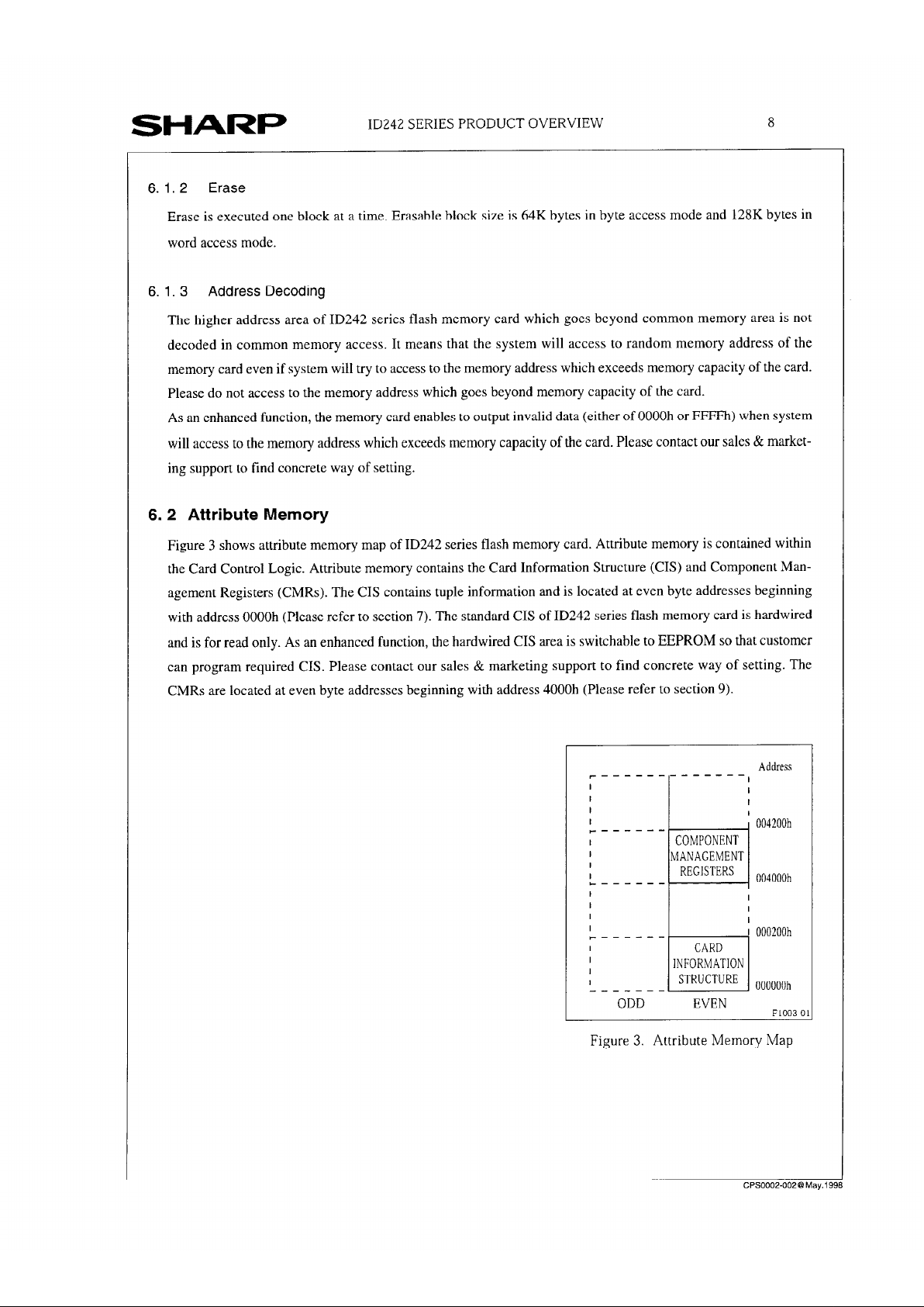
Figure 3 shows attribute memory map of ID242 series flash memory card. Attribute memory is contained within
the Card Control Logic. Attribute memory contains the Card Information Structure (CIS) and Component Management Registers (CMRs). The CIS contains tuple information and is located at even byte addresses beginning
with address OOOOh (Please refer to section 7). The standard CIS of ID242 series flash memory card is hardwired
and is for read only. As an enhanced function, the hardwired CIS area is switchable to EEPROM so that customer
can program required CIS. Please contact our sales & marketing support to find concrete way of setting. The
CMRs are located at even byte addresses beginning with address 4000h (Please refer to section 9).
Address
r-------------,
I
I
I
I
I
I
' 004200h
r-----I
COMPONENT
I
MANAGEMENT
I
I
REGISTERS
c------
_ 004000h
I
I
I
I
I
r------
I 000200h
I
CARD
I
I
INFORMATION
I
STRUCTURE OOOOOOh
------ODD EVEN
F1003-01
Figure 3. Attribute Memory Map
CPSOOOZ-002@ May. 1998

SHARI=
ID242SERIESPRODUCTOVERVIEW
6.3 Function Table
6.3.1 Common Memory Access
Table 4. Common Memory Access
6.3.2 Attribute Memory Access
Table 5. Attribute Memory Access
XXX:Output data is invalid.
The standard CIS is for read only. Write operation is only for CMRs and CIS on EEPROM
7. Card Information Structure (CIS)
The CIS is contained within attribute memory (Please refer to section 6.2). Table 6 shows standard CIS tuples, but
it is for read only. As an enhanced function, the hardwired CIS area is switchable to EEPROM so that customer
can program required CIS. Please contact our sales & marketing support to find concrete way of setting.
 Loading...