

Page 1
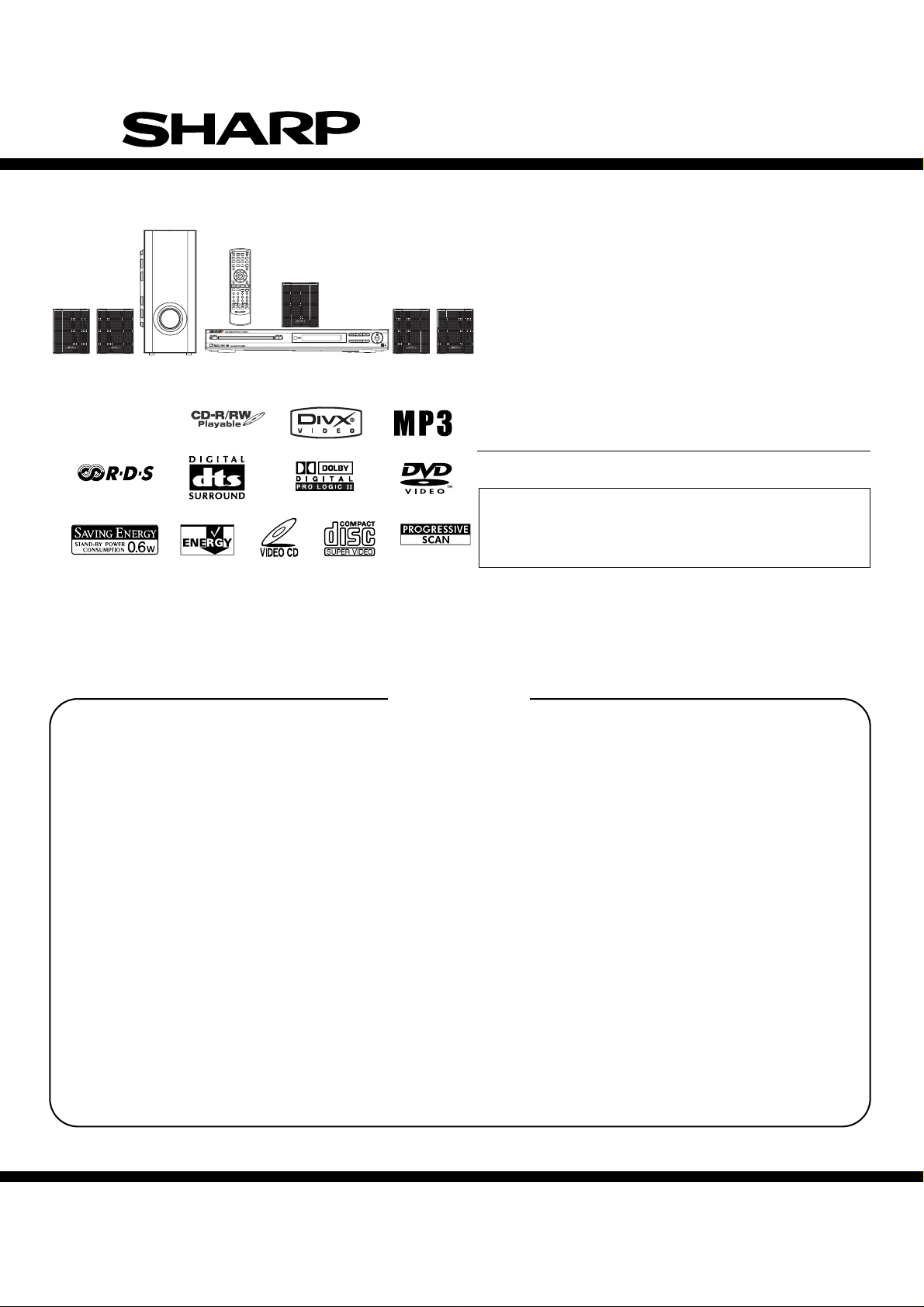
HT-CN410DVH
SERVICE MANUAL
No. S9501HTN410DV
Home Theater with DVD
MODEL
• In the interests of user-safety (Required by safety regulations in some countries) the set should be restored to its
original condition and only parts identical to those specified
be used.
HT-CN410DVH
(For Europe)
CONTENTS
Page
SPECIFICATIONS..................................................................................................................................................................4
LASER BEAM SAFETY PRECAUTIONS ..............................................................................................................................6
IMPORTANT SAFEGUARDS AND PRECAUTIONS.............................................................................................................7
STANDARD NOTES FOR SERVICING.................................................................................................................................7
OPERAT ING CONTROLS AND FUNCTIONS......................................................................................................................10
TROUBLESHOOTING..........................................................................................................................................................13
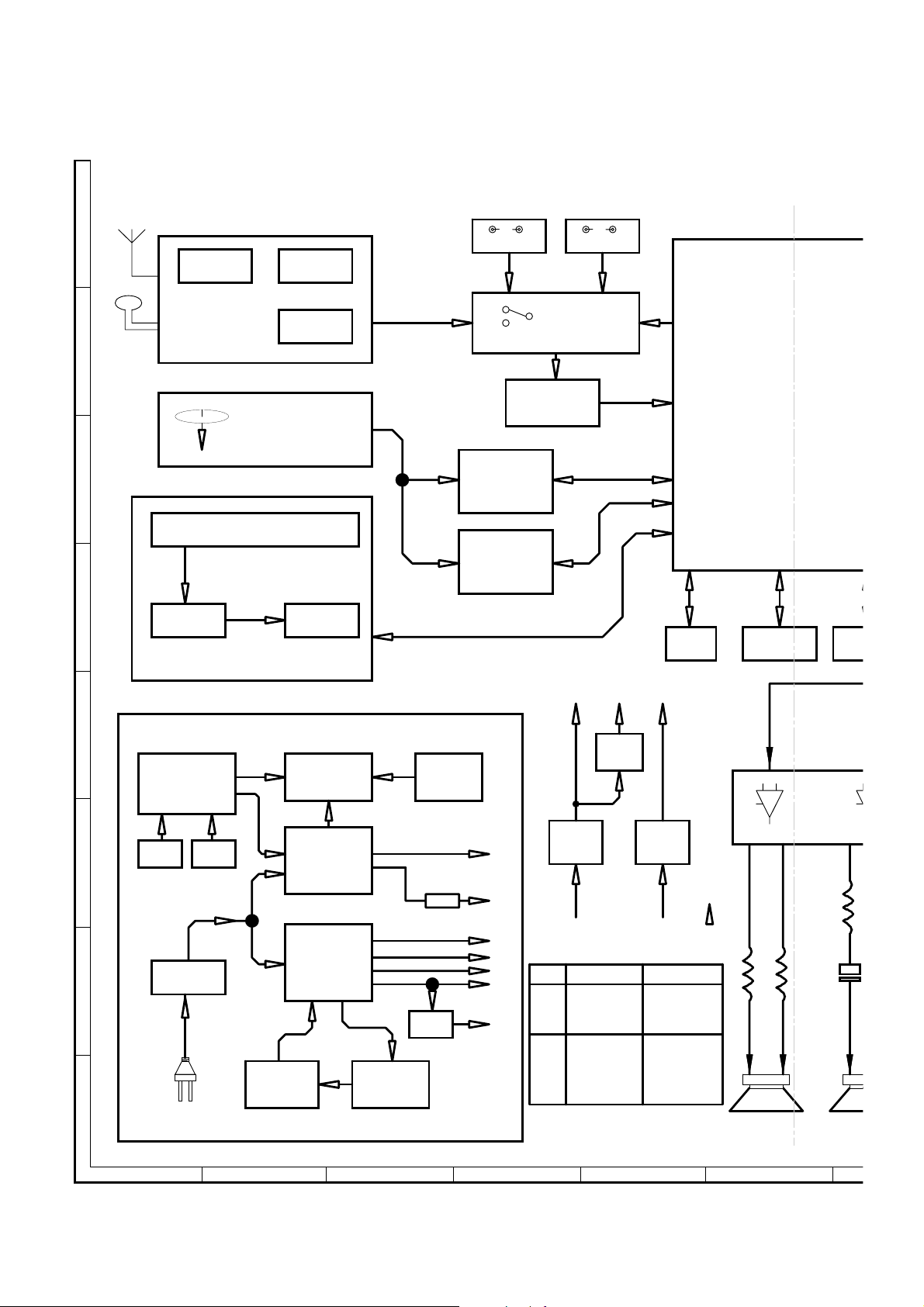
BLOCK DIAGRAMS..............................................................................................................................................................14
SCHEMATIC DIAGRAMS / IC’S PIN VOLTAGE...................................................................................................................16
WAVEFORMS.......................................................................................................................................................................28
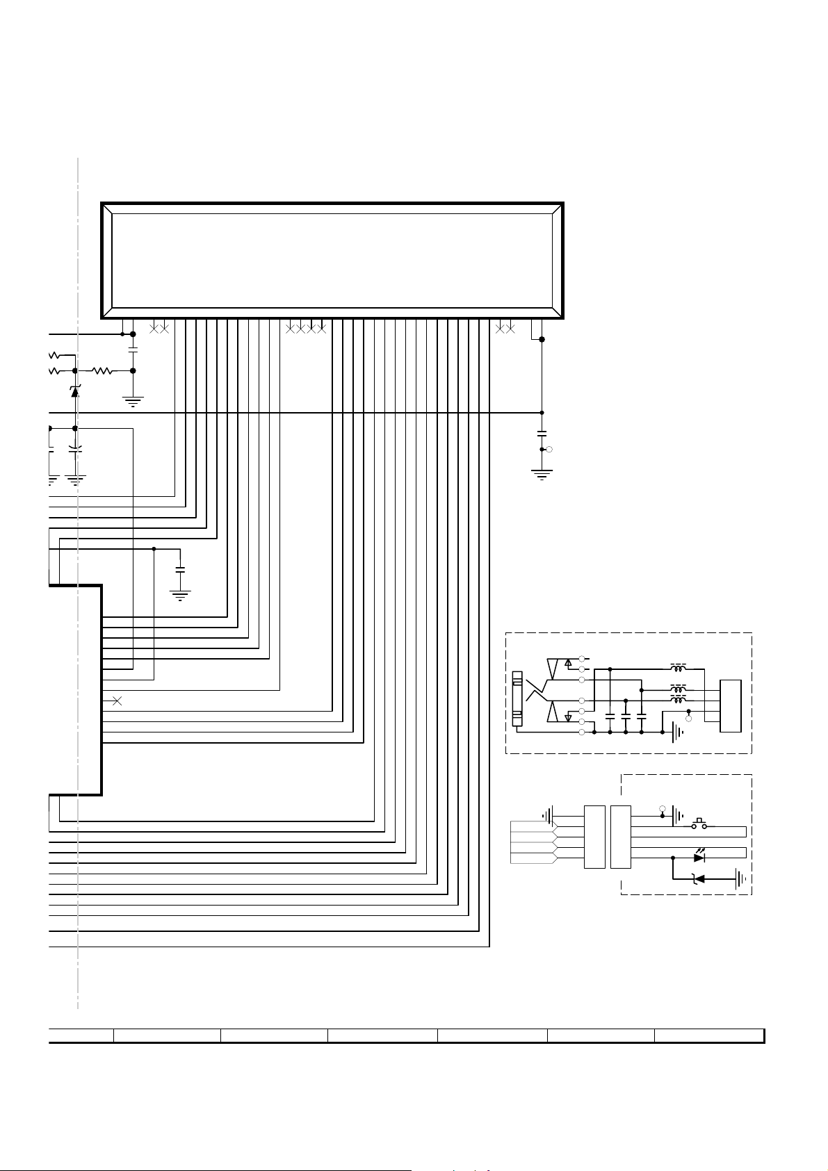
WIRING DIAGRAM...............................................................................................................................................................31
IC PIN FUNCTION DESCRIPTIONS....................................................................................................................................38
FL DISPLAY..........................................................................................................................................................................65
PARTS GUIDE
SHARP CORPORATION
1
This document has been published to be used for
after sales service only.
The contents are subject to change without notice.
Page 2
HT-CN410DVH
CHAPTER 1. GENERAL DESCRIPTION
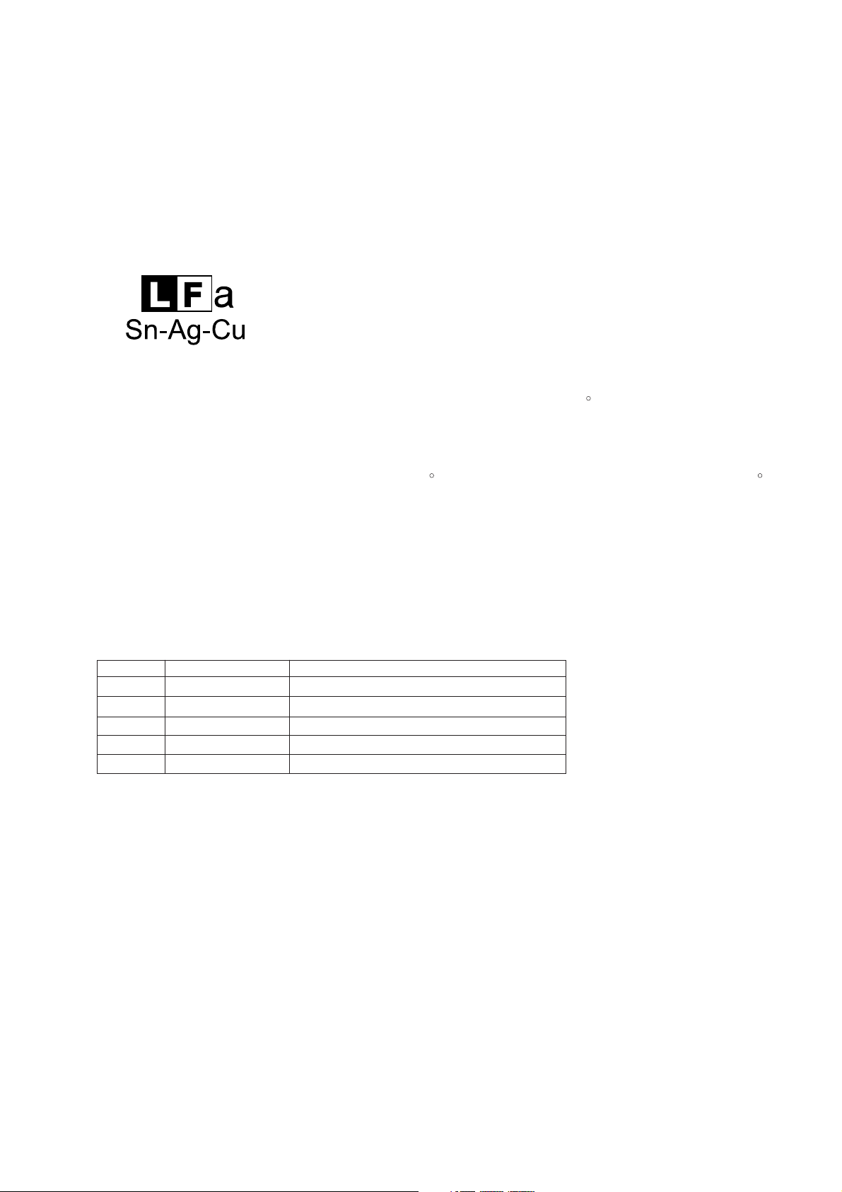
[1] PRECAUTION FOR USING LEAD-FREE SOLDER
1. Employing lead-free solder
"MAIN,DISPLAY,TERMINAL,SWITCH,POWER,JACK,TUNER,DVD,MICVIDEOOUT,CDCHANGERMOTOR(PWBONLY),
LED PWB" of this model employs lead-free solder.
The LF symbo lindicates lead-free solder,and is attached on the PWB and service manuals.The alphabetical character
following LF shows the type of lead-free solder.
Example:
Indicates lead-free solder of tin,silver and copper.
2. Using lead-free wire solder
When fixing the PWB soldered with the lead-free solder,apply lead-free wire solder. Repairing with conventional lead wire solder
may cause damage or accident due to cracks.
As the melting point of lead-free solder (Sn-Ag-Cu) is higher than the lead wire solder by 40 C, were commend you to use a
dedicated soldering bit,if you are not familiar with how to obtain lead-free wire solder or soldering bit, contact our service station
or service branch in your area.
3. Soldering
As the melting point of lead-free solder (Sn-Ag-Cu) is about 220 C which is higher than the conventional lead solder by 40 C,
and as it has poor solder wettability,you may be apt to keep the soldering bit in contact with the PWB for extended period of
time. However, Since the land may be peeled off or the maximum heat-resistance temperature of parts may be exceeded,
remove the bit from the PWB assoonas you confirm the steady soldering condition.
Lead-free solder contains more tin, and the end of the soldering bit may be easily corrected. Make sure to turn on and off the
power of the bit as required.
If a different type of solder stays on the tip of the soldering bit, it is alloyed with lead-free solder. Clean the bit after every use
of it.
When the tip of the soldering bit is blackened during use, file it with steel wool or fine sandpaper.
Be careful when replacing parts with polarity indication on the PWB silk.
Lead-free wire solder for servicing
Ref No.
PWB-A1
PWB-A2
PWB-A3 92LABE10530201
PWB-B
PWB-C
Parts No.
92LABE10530101
92LABE10530301
92LABE10510003
92LABE10504004
CONTROL PWB ASS'Y
EARPHONE PWB ASS'Y
STANDBY PWB ASS'Y
MAIN PWB ASS'Y
POWER PWB ASS'Y
Description
2
Page 3
HT-CN410DVH
SAFETY PRECAUTION FOR SERVICE MANUAL
Precaution to be taken when replacing and servicing the
Laser Pickup.
The AEL (Accessible Emission Level) of Laser Power Output
for this model is specified to be lower than Class 1 Requirements. However, the following precautions must be observed
during servicing to protect your eyes against exposure to the
Laser beam.
(1) When the cabinet has been removed, the power is turned
on without a compact disc, and the Pickup is on a position
outer than the lead-in position, the Laser will light for several seconds to detect a disc. Do not look into the Pickup
Lens.
(2) The Laser Power Output of the Pickup inside the unit and
replacement service parts have already been adjusted prior
to shipping.
(3) No adjustment to the Laser Power should be attempted
when replacing or servicing the Pickup.
(4) Under no circumstances look directly into the Pickup Lens
at any time.
(5) CAUTION - Use of controls or adjustments, or performance
of procedures other than those specified herein may result
in hazardous radiation exposure.
Laser Diode Properties
Material: AlGaAs/AlGalnP
Wavelength: 785 nm/650 nm
Emission Duration: continuous
Laser Output: max. 0.6 mW
CAUTION: VISIBLE AND INVISIBLE LASERRADIATION WHEN
OPEN. DO NOT STARE INTOBEAM OR VIEW DIRECTLY WITH
OPTICAL INSTRUMENTS.
WARNUNG: SICHTBARE UND UNSICHTBARE LASERSTRAHLUNG
WENN GERÄT GEÖFFNET. NICHT INDIE STRAHLUNG SCHAUEN
ODER DIREKT MIT OPTISCHEN HILFSMITTELNBETRACHTEN.
ATTENTION: RAYONS LASER VISIBLE ETINVISIBLE EN CAS
D'OUVERTURE. NE PAS REGARDER LEFAISCEAU DIRECTEMENT
OU AVEC DES INSTRUMENTS OPTIQUES.
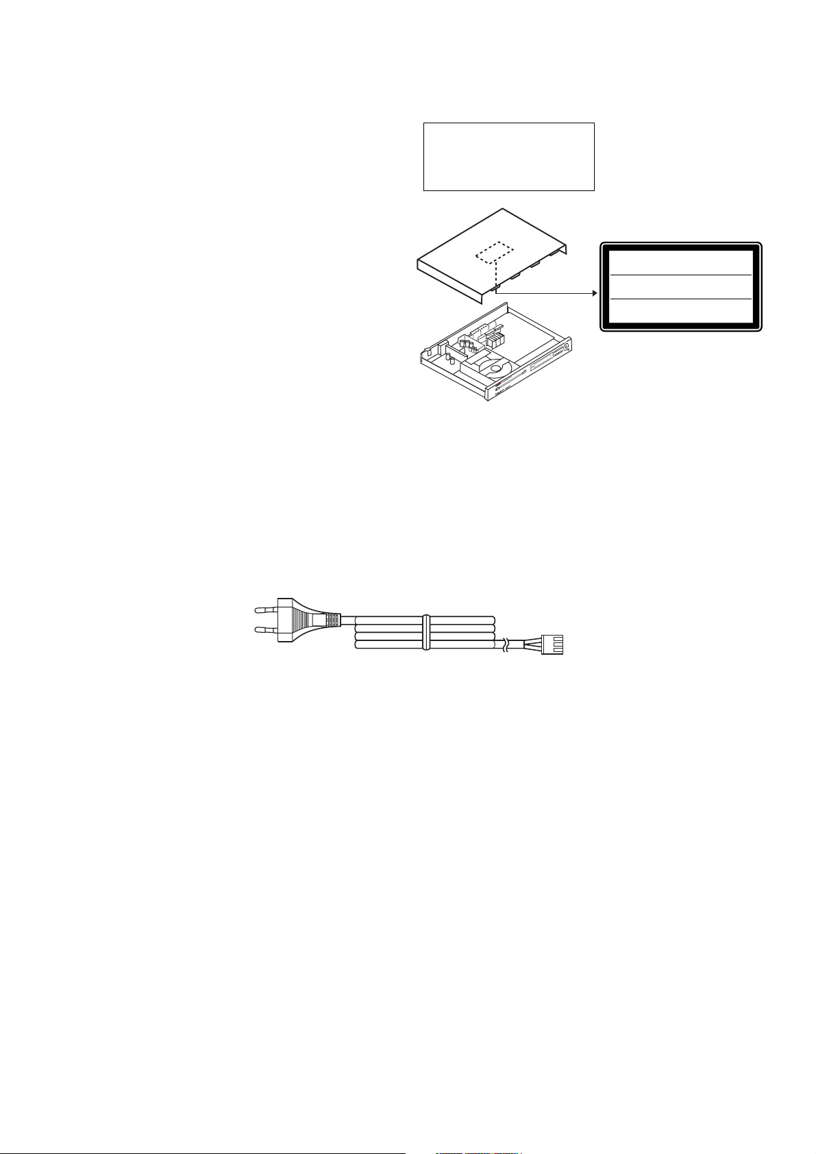
AC POWER SUPPLY CORD
92LVPE1K327210
3
Page 4
HT-CN410DVH
SPECIFICATIONS
As part of our policy of continuous improvement, SHARP reserves the right to make design and specification changes
for product improvement without prior notice. The performance specification figures indicated are nominal values of
production units. There may be some deviations from these values in individual units.
l General
Power source AC 230 V, 50 Hz
Power consumption
Dimensions
Weight 3.8 kg
Audio input terminals Analogue input (IN 1): RCA type × 1 pair (L/R)
Audio output terminals
Video output terminals
Video output terminals SCART output: SCART terminal x 1
Power on: 45 W
Power stand-by:0.6W
Width: 428 mm
Height: 55 mm
Depth: 360 mm
Analogue input (IN 2): RCA type × 1 pair (L/R)
Analogue output (OUT): RCA type × 1 pair (L/R)
Headphone: 16-50 ohms (recomended: 32 ohms)
Digital output: Caoxial type x 1
S-video output: S-terminal × 1
Video output: RCA type × 1
Component video output: P
B, PB, Y
l Amplifier (HT-CN410DVH)
Output power Front speakers: RMS: 42 W (21 W + 21 W) (DIN 45 324)
Centre speaker: RMS: 21 W (DIN 45 324)
Surround speakers: RMS: 42 W (21 W + 21 W) (DIN 45 324)
Subwoofer speaker: RMS: 45 W (DIN 45 324)
l DVD player
Signal system PAL/NTSC colour
Supported disc types
Video signal Horizontal resolution: 525 lines S/N ratio: 56 dB
Audio signal Frequency characteristics Linear PCM DVD: 20 Hz to 20 kHz
DVD (with the same region number on the back of the unit or ALL), SVCD, VCD, audio CD,
CD-R, CD-RW, MP3
(sampling rate: 48 kHz)
20 Hz to 20 kHz
(sampling rate: 96 kHz)
CD: 20 Hz to 20 kHz
S/N ratio CD: 65 dB (1 kHz)
Dynamic range Linear PCM DVD: 95 dB CD: 94 dB
Total harmonic distortion ratio 0.2 % maximum
l Tuner
Frequency range FM: 87.5 - 108 MHz
AM: 522 - 1620 kHz
4
Page 5
l Front speakers
Type Full range speaker system (magnetic shield)
7 cm speaker
Maximum input power 30 W
Impedance 4 ohms
Dimensions Width: 90 mm
Height: 110 mm
Depth: 100 mm
Weight 0.46 kg/each
l Surround speakers
Type Full range speaker system
7 cm speaker
Maximum input power 30 W
Impedance 4 ohms
Dimensions Width: 90 mm
Height: 110 mm
Depth: 100 mm
HT-CN410DVH
Weight 0.45 kg/each
l Center speaker
Type Full range speaker system
7 cm speaker
Maximum input power 30 W
Impedance 4 ohms
Dimensions Width: 90 mm
Height:110 mm
Depth: 100 mm
Weight 0.46 kg
l Subwoofer
Type Subwoofer system
13 cm Subwoofer
Maximum input power 60 W
Impedance 8 ohms
Dimensions Width:132 mm
Height: 282 mm
Depth: 330 mm
Weight 2.8 kg
5
Page 6
HT-CN410DVH
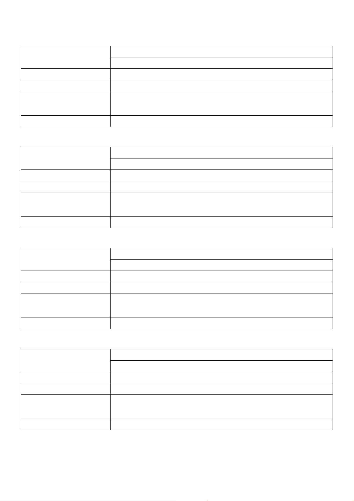
LASER BEAM SAFETY PRECAUTIONS
This DVD player uses a pickup that emits a laser beam.
Do not look directly at the laser beam coming
from the pickup or allow it to strike against
your skin.
The laser beam is emitted from the location shown in the figure. When checking the laser diode, be su re to keep your eyes at least
30cm away from the pickup lens when the diode is turned on. Do not look directly at the laser beam.
Caution: Use of controls and adjustments, or doing procedures other than those specified herein, may result in hazardous radiation
exposure.
Drive Mecha Assembly
Laser Beam Radiation
Laser Pickup
Turntable
6
Page 7
STANDARD NOTES FOR SERVICING
HT-CN410DVH
How to Remove / Install Flat Pack-IC
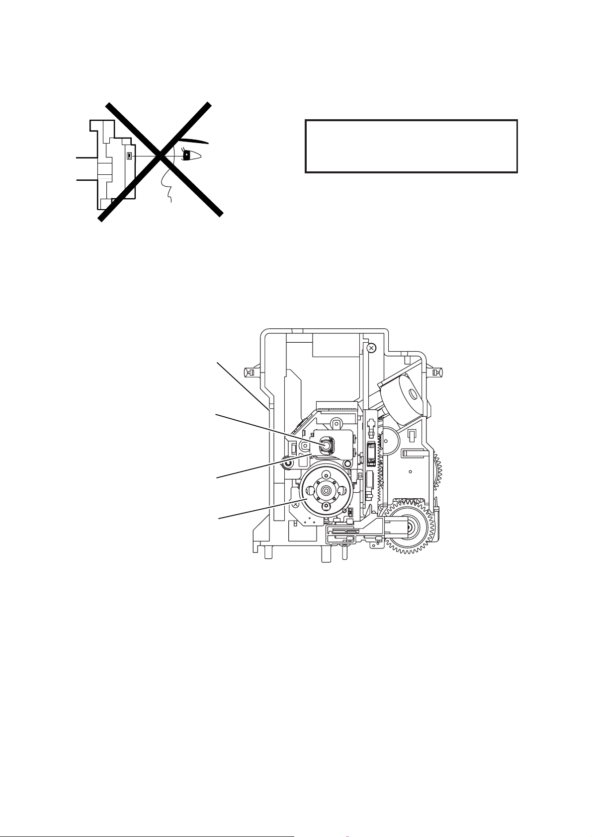
1. Removal
With Hot-Air Flat Pack-IC Desoldering Machine:
(1) Prepare the hot-air flat pack-IC desoldering ma-
chine, then apply hot air to the Flat Pack-IC (about 5
to 6 seconds). (Fig. S-1-1)
Fig. S-1-1
(2) Remove the flat pack-IC with tweezers while apply-
ing the hot air.
(3) Bottom of the flat pack-IC is fixed with glue to the
CBA; when removing entire flat pack-IC, first apply
soldering iron to center of the flat pack-IC and heat
up. Then remove (glue will be melted). (Fig. S-1-6)
(4) Release the flat pack-IC from the CBA using twee-
zers. (Fig. S-1-6)
Caution:
1. Do not supply hot air to the chip parts around the flat
pack-IC for over 6 seconds because damage to the
chip parts may occur. Put masking tape around the
flat pack-IC to protect other parts from damage.
(Fig. S-1-2)
2. The flat pack-IC on the CBA is affixed with glue, so
be careful not to break or damage the foil of each pin
or the solder lands under the IC when removing it.
Hot-air
Flat Pack-IC
Desoldering
CBA
Masking
Tape
Tweezers
Machine
Flat Pack-IC
Fig. S-1-2
With Soldering Iron:
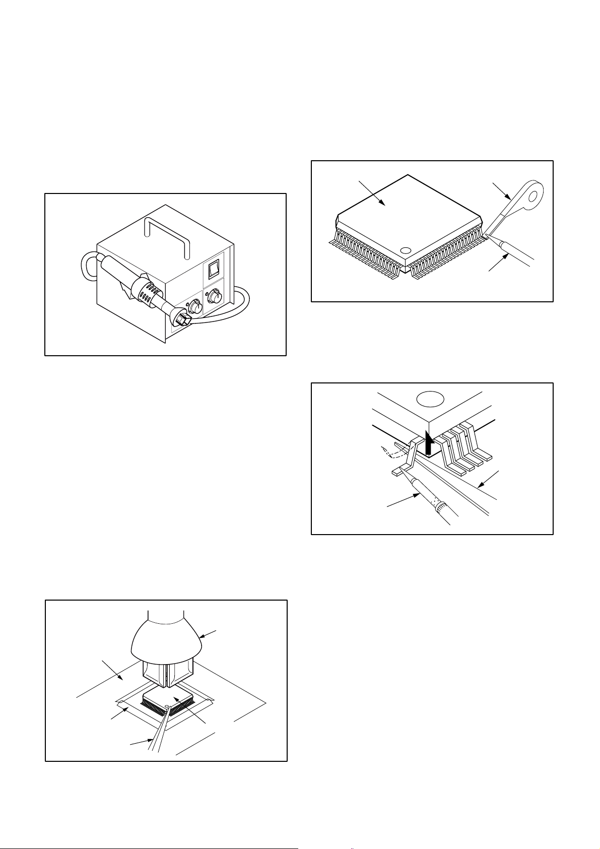
(1) Using desoldering braid, remove the solder from all
pins of the flat pack-IC. When you use solder flux
which is applied to all pins of the flat pack-IC, you can
remove it easily. (Fig. S-1-3)
Flat Pack-IC
(2) Lift each lead of the flat pack-IC upward one by one,
using a sharp pin or wire to which solder will not
adhere (iron wire). When heating the pins, use a fine
tip soldering iron or a hot air desoldering machine.
(Fig. S-1-4)
Fine Tip
Soldering Iron
(3) Bottom of the flat pack-IC is fixed with glue to the
CBA; when removing entire flat pack-IC, first apply
soldering iron to center of the flat pack-IC and heat
up. Then remove (glue will be melted). (Fig. S-1-6)
(4) Release the flat pack-IC from the CBA using twee-
zers. (Fig. S-1-6)
Desoldering Braid
Soldering Iron
Fig. S-1-3
Sharp
Pin
Fig. S-1-4
With Iron Wire:
(1) Using desoldering braid, remove the solder from all
pins of the flat pack-IC. When you use solder flux
which is applied to all pins of the flat pack-IC, you can
remove it easily. (Fig. S-1-3)
(2) Affix the wire to a workbench or solid mounting point,
as shown in Fig. S-1-5.
(3) While heating the pins using a fine tip soldering iron
or hot air blower, pull up the wire as the solder melts
so as to lift the IC leads from the CBA contact pads
as shown in Fig. S-1-5.
7
Page 8
HT-CN410DVH
(4) Bottom of the flat pack-IC is fixed with glue to the
CBA; when removing entire flat pack-IC, first apply
soldering iron to center of the flat pack-IC and heat
up. Then remove (glue will be melted). (Fig. S-1-6)
(5) Release the flat pack-IC from the CBA using twee-
zers. (Fig. S-1-6)
Note:
When using a soldering iron, care must be taken to
ensure that the flat pack-IC is not being held by glue.
When the flat pack-IC is removed from the CBA,
handle it gently because it may be damaged if force
is applied.
Hot Air Blower
or
Iron Wire
Soldering Iron
2. Installation
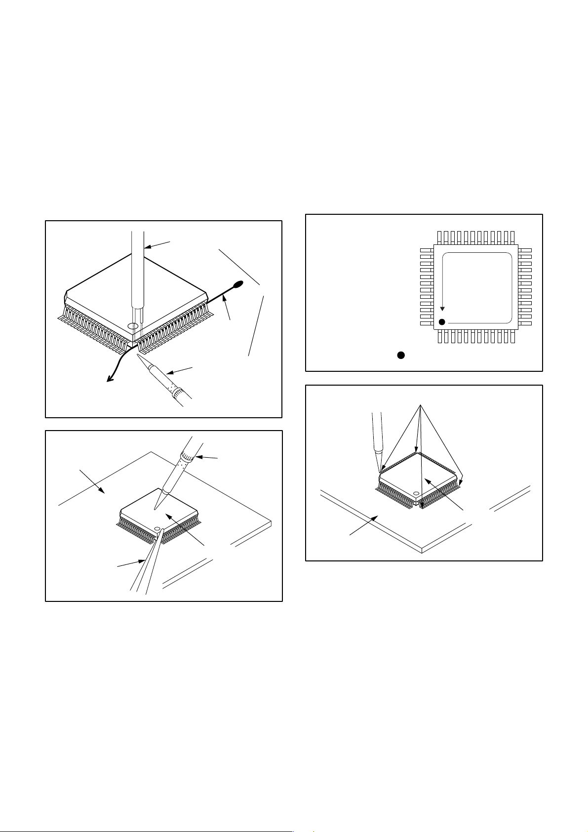
(1) Using desoldering braid, remove the solder from the
foil of each pin of the flat pack-IC on the CBA so you
can install a replacement flat pack-IC more easily.
(2) The "●" mark on the flat pack-IC indicates pin 1. (See
Fig. S-1-7.) Be sure this mark matches the 1 on the
PCB when positioning for installation. Then presolder the four corners of the flat pack-IC. (See Fig. S1-8.)
(3) Solder all pins of the flat pack-IC. Be sure that none
of the pins have solder bridges.
Example :
Pin 1 of the Flat Pack-IC
is indicated by a " " mark.
Fig. S-1-7
To Solid
Mounting Point
CBA
Tweezers
Fig. S-1-5
Fine Tip
Soldeing Iron
Flat Pack-IC
Fig. S-1-6
Presolder
Flat Pack-IC
CBA
Fig. S-1-8
8
Page 9
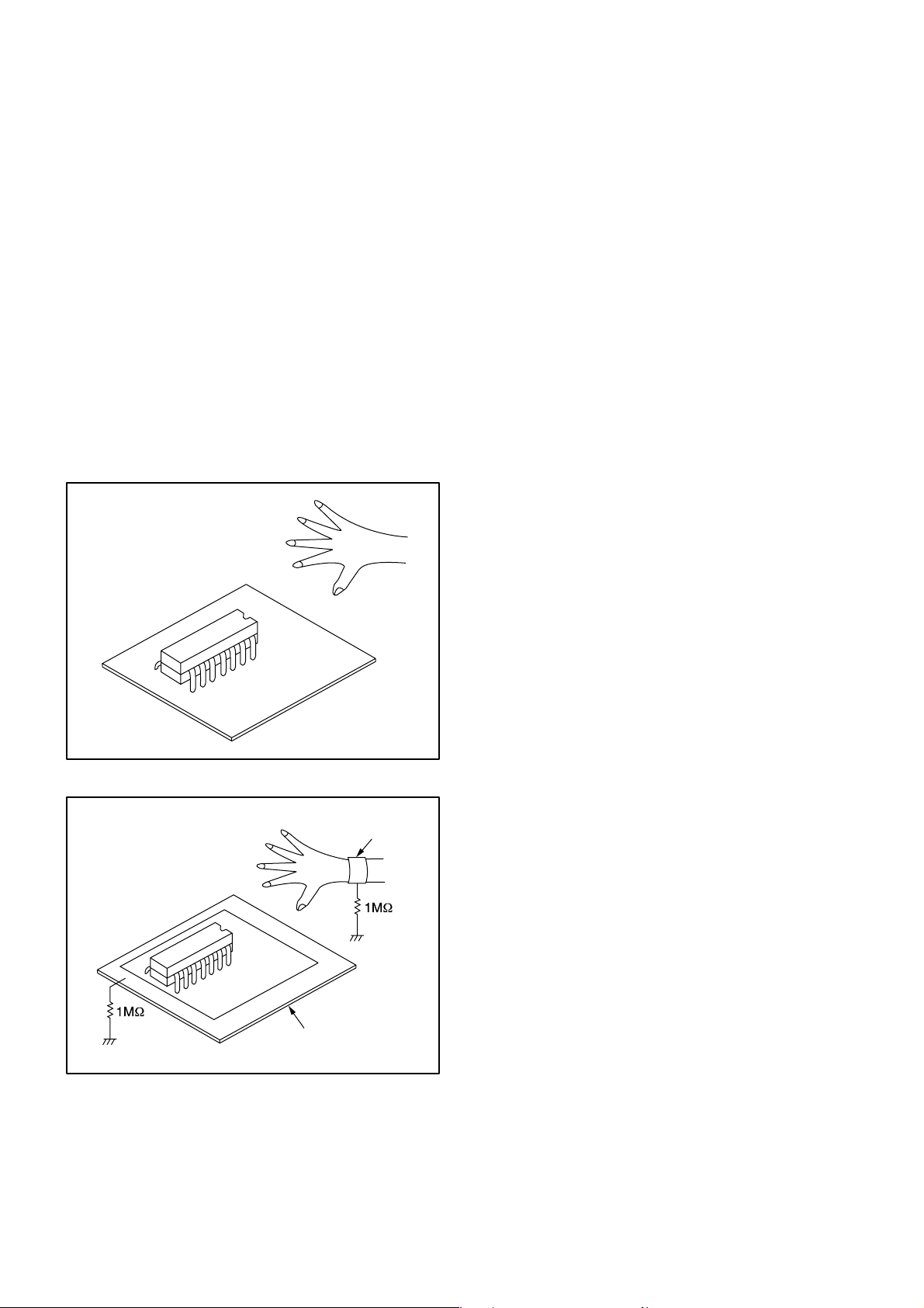
Instructions for Handling
Semi-conductors
Electrostatic breakdown of the semi-conductors may
occur due to a potential difference caused by electrostatic
charge during unpacking or repair work.
1. Ground for Human Body
Be sure to wear a grounding band (1MΩ) that is properly
grounded to remove any static electricity that may be
charged on the body.
2. Ground for Workbench
Be sure to place a conductive sheet or copper plate with
proper grounding (1MΩ) on the workbench or other
surface, where the semi-conductors are to be placed.
Because the static electricity charge on clothing will not
escape through the body grounding band, be careful to
avoid contacting semi-conductors with your clothing.
< Incorrect >
HT-CN410DVH
< Correct >
CBA
Grounding Band
CBA
Conductive Sheet or
Copper Plate
9
Page 10
HT-CN410DVH
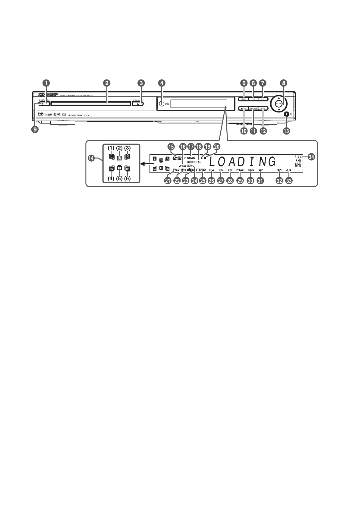
OPERATING CONTROLS AND FUNCTIONS
n Main unit (front panel)
1. On/Stand-by Button
2. Disc Tray
3. Disc Tray Open/Close Button
4. Remote Sensor
5. Play or Pause Button
6. Chapter (track) Skip Down or Preset/Tuning Down Button
7. Chapter (track) Skip Up or Preset/Tuning Up Button
8. Volume Up and Down or Speaker Level Adjust Buttons
9. Power Stand-by Indicator
10. Stop Button
11. Function Button
12. Speaker Level Mode Button
13. Headphone socket
14. Speaker Indicators
(1) Left Front Speaker Indicator
(2) Centre Speaker Indicator
(3) Right Front Speaker Indicator
(4) Left Surround Speaker Indicator
(5) Subwoofer Indicator
(6) Right Surround Speaker Indicator
15. DVD Indicator
16. JPEG Indicator
17. P - SCAN mode
18. Dolby Digital Signal Indicator
19. Play Indicator
20. Pause Indicator
21. SVCD/VCD/CD Indicator
22. MP3 Indicator
23. DTS Signal Indicator
24. Dolby Pro Logic/Pro Logic II Indicator
25. Stereo (2-ch) or FM Stereo Receiving Indicator
26. Title Indicator
27. Track Indicator
28. Chapter Indicator
29. Tuner Preset Indicator
30. Programme Indicator
31. Sleep Indicator
32. Repeat Indicator
33. A - B Repeat Indicator
34. RDS Indicator
10
Page 11
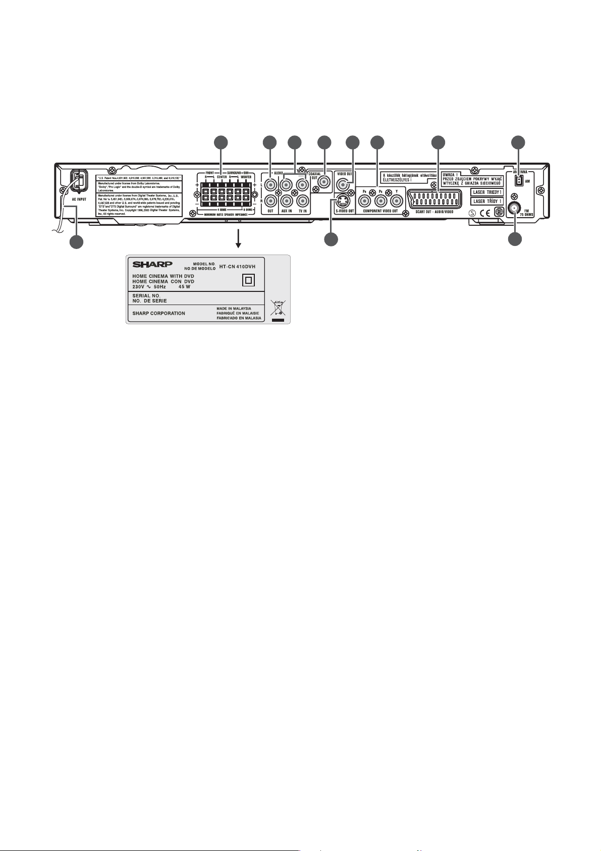
OPERATING CONTROLS AND FUNCTIONS
n Main unit (rear panel)
HT-CN410DVH
1
1. AC Power Lead
2. Speaker Terminals
3. Audio Output Sockets
4. Audio Input Sockets (TV/AUX)
5. Digital Output Socket (Coaxial)
6. Video Output Socket
7. Component Video Output Socket
8. SCART Output Socket (Audio + Video)
<The bottom of the unit>
2 84
3 5
10
76 9
11
9. AM Loop Aerial Socket
10. S-video Output Socket
11. FM 75 Ohms Aerial Socket
11
Page 12
HT-CN410DVH
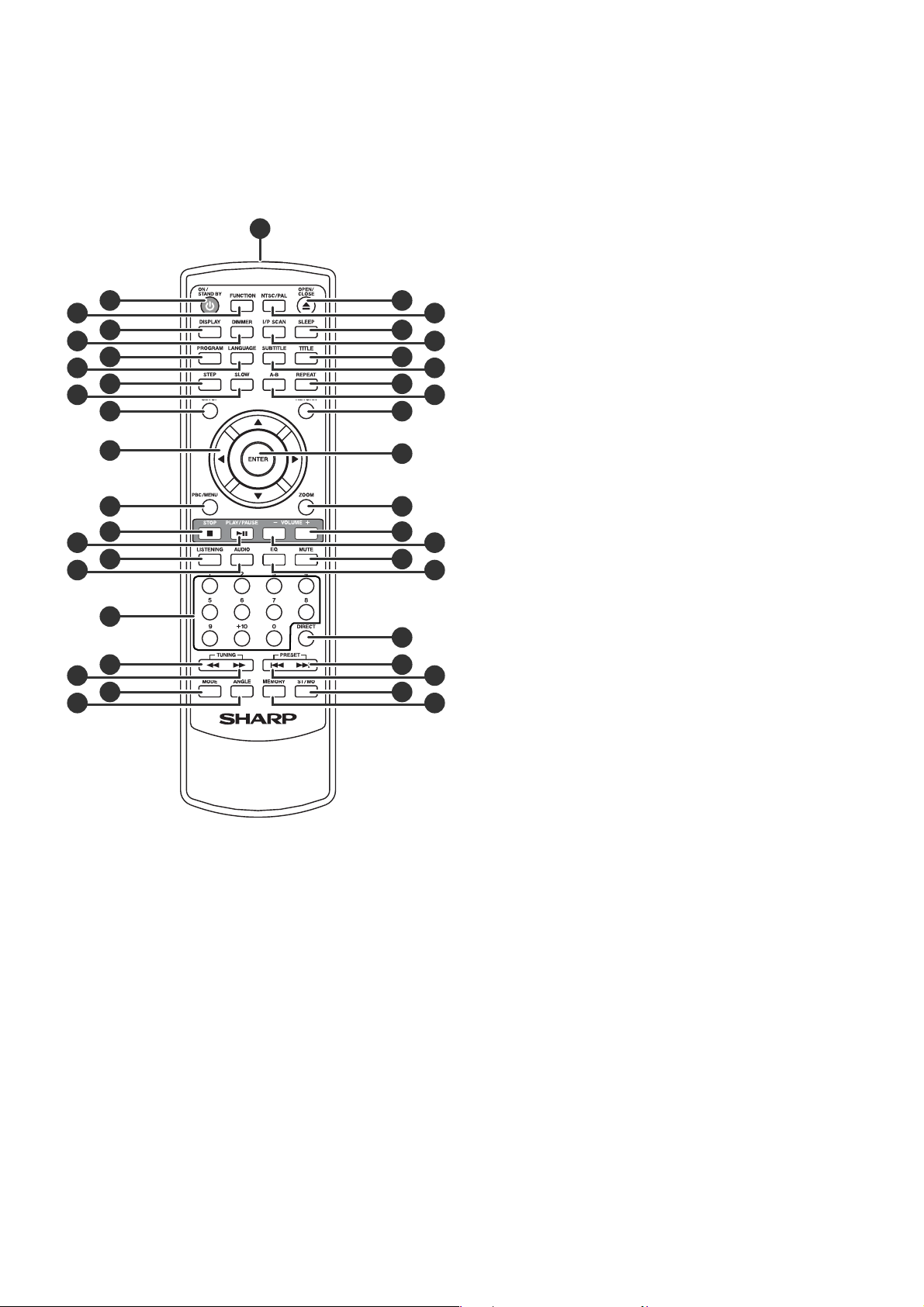
n Remote Control
2
3
4
5
6
7
8
9
10
11
12
13
14
15
16
17
18
19
20
21
1. Remote Control Transmitter
2. On/Stand-by Button
3. Function Button
4. Display Button
1
22
23
24
25
26
27
28
29
30
31
32
33
34
35
36
37
38
39
40
41
5. Dimmer
6. Program Button
7. Language Select Button
8. Frame Advance Button (Step Function)
9. Slow Motion Button
10. Setup Menu Button
11. Cursor Buttons
12. PBC/MENU Button
13. Stop Button
14. Play or Pause Button .
15. Surround/Stereo (2-ch) Listening Mode Button
16. Audio Select Button.
17. Direct Number Buttons
18. Fast Reverse or Tuning Down Button
19. Fast Forward or Tuning Up Button
20. Speaker Level Mode Button
21. Angle Select Button
22. Disc Tray Open/Close Button
23. NTSC/PAL Select Button
24. Sleep Button
25. Interlace and Progressive Scan Button
26. Title Select Button
27. Subtitle Select Button
28. Repeat Play Button
29. A - B Repeat Button
30. Return Button
31. Enter Button
32. Zoom Button
33. Volume adjust up Button
34. Volume adjust down Button
35. Mute Button
36. EQ (equaliser) Button
37. Direct Button
38. Chapter (track) Skip Up or Preset Up Button
39. Chapter (track) Skip Down or Preset Down Button
40. FM Stereo/Mono Select Button
41. Memory Button
12
Page 13

TROUBLESHOOTING
HT-CN410DVH
If you experience any of the following difficulties while
using the system, use troubleshooting guide to help you
remedy the problem. Should any problem persist,
consult your nearest service center.
No power:
l Is the power cord firmly plugged into the power out-
let?
l One of the safety mechanisms may be operating. In
this event, unplug the player from the power outlet
briefly and then plug it in again.
No picture:
l Check that the system is connected securely.
l The video connecting system coed is damaged.
Replace it with a new one.
l Make sure you connect the system to video input con-
nector on the TV.
l Make sure you turn on the TV.
l Make sure you select the video input on the TV so
that you can view the pictures from this syste m .
The picture noise appears:
l Clear the disc.
l If video from this system has to go through your VCR
to get too your TV, the copy-protection applied to
some DVD programs could affect picture quality. If
you still experience problems after checking your connections, please try connecting your DVD system
directly to your TV's S-Video input, if your TV is
equipped with this input.
The aspect ratio of the screen cannot be
changed even though you set "TV DISPLAY" in
the SETUP menu when you play a wide picture:
l The aspect rate is fixed on your DVD disc.
l If you connect the system with the S-Video cable,
connect directly to the TV. Otherwise, you may not
change the aspect rate.
l Depending on the TV, you may not change the aspect
rate.
There is no sound or only a very low-level
sound is heard:
l Check that the speakers and components are con-
nected securely.
l Make sure that you have selected the correct source
on the system.
l The protective device on the system has been acti-
vated because of a short circuit. Turn off the system,
eliminate the short-circuit problem and turn on the
power again.
l The audio connecting cord is damaged. Replace it
with a new one.
l The system or fast reverse is performed. Press PLAY/
PAUSE 3 /8 to return to normal play mode.
l Check the speaker settings.
The left and right sounds are unbalanced or
reversed:
l Check that the speakers and components are con-
nected correctly and securely.
l Adjust front balance parameter using SELECT and
VOLUME +/-.
Severe hum or noise is heard:
l Check that the speakers and components are con-
nected correctly and securely.
l Check that the connecting cords are away from a
transformer or motor, and at least 3 meters away from
a TV set or fluorescent light.
l Move your TV away from the audio components.
l The plugs and jacks are dirty, wipe them with a cloth
slightly moistened with alcohol.
l Clear the disc.
The sound losses stereo effect when you play a
Video CD or a CD:
l Set the Audio mode to "STEREO" in the SETUP
menu.
l Make sure you connect the system appropriately.
l The surround effect is difficult to hear when you are
playing a Dolby Digital sound track.
l Check the speaker connections.
l Depending on the DVD disc, the output signal may
not be the entire 5.1 channel but monaural or stereo
even if the sound track is recorded in Dolby Digital
format.
The sound comes from the center speaker only:
l Depending on the disc, the sound may come from the
center speaker only.
No sound is heard from the center speaker:
l Make sure the Center is set to "ON" in SETUP menu.
l You may set the listening mode to Dolby Pro Logistic
Phantom.
l Adjust the speaker volume.
No sound or only a very low-level sound is
heard from the rear speakers:
l Make sure the rear is set to "ON" in SETUP menu.
l Adjust the speaker volume.
The language for the subtitles cannot be
changed when you play a DVD:
l Multilingual subtitles are not recorded on the DVD.
l Changing the language for the subtitles is prohibited
on the DVD.
The subtitles cannot turn off when you play a
DVD:
l Depending on the DVD, you may no t be able to turn
the subtitles off.
The angles cannot be changed when you play a
DVD:
l Multi-angles are not recorded on the DVD.
l Change the angles when the angle mark appears on
the TV screen.
l Changing the angles is prohibited on the DVD.
The system does not operate properly:
l Static electricity, etc., may affect the system's opera-
tion.
l Press the POWER button to turn off, then press again
to turn on.
13
Page 14
HT-CN410DVH
A
B
C
D
E
F
G
H
1
23456
-
TUNER PACK IC TEA5762H
IC SAA6588T
(RDS)
TUNER SYSTEM
DVD LOADER
SANYO DVD LODER
VFD
IC V63111
VFD CONTROL
KEY
KEY CONN SYSTEM
TV-IN AUX-IN
IC TC4052BP
SWITCH
A/D
CS5342
IC ESS6602
DVD RF
IC AM5869S
DVD PACK DRIVER
ES680
u_COM
SDARM
4Mx16
IC AT24C02
SERIAL EEPROM
MBM29
EPR
L1
C1
IC1 STA518
DIGITAL POWER AM
SUB SPK
CS
Notice:R1-R11=0R
L1-L10=30UH
C1-C6=0R
L2 L3L4 L5
L6 L8 L10
R6 R8 IC2
C1-C6=470U
R1 R3 R5 R7
R9 R11 R2 R4
L2 L3L4 L5
L6 L8 L10
R6 R8 IC2
R1 R3 R5 R7
R9 R11 R2 R4
200W
300W
+12V
+5V IN
2SC945
2SB772
2SA952
3.3V OUT
+1.8V OUT
Phone 5V OUT
POWER SUPPLY
TRANSFORMER
IC KA7500C IC BA4558D
MOSFET MOSFET
TRANSFORMER
TRANSFORMER
BRIDGE
REGULATOR
IC FSDL0165RN
IC EL817C
MOSFET
AC 220V
+27V
VFD
-27V
+12V
AC1
AC2
BK5V
+5V
Delet
Add
+- +
BLOCK DIAGRAM
FIGURE 1. BLOCK DIAGRAM (1/2)
14
Page 15
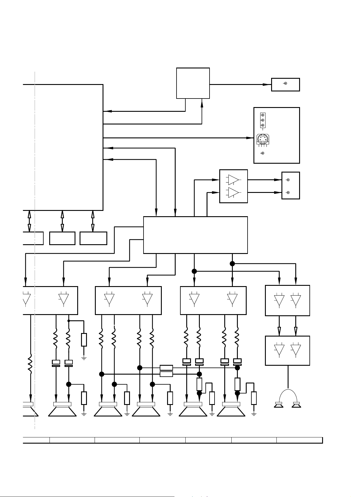
Logic HEX Inverter
IC SN7404
HT-CN410DVH
COAXIAL OUT
Y.U.V OUT
(OR SCART)
ES6809
u_COM
AT24C02
IAL EEPROM
DIGITAL POWER AMP
IC1 STA518
MBM29LV800BA
EPROM
IC 74HC374
I/O PIN EXPAND
IC2 STA518
DIGITAL POWER AMP
IC STA308-A
DIGITAL AUDIO PROCESSOR
Bilt IN TREBLE BASS EQ
VOLUME CONTROL
FR
IC3 STA518
DIGITAL POWER AMP
FL
S-VIDEO
C-VIDEO
IC IRC4558
LINES OUT
AMPLIFIER
IC IRC4558
AMPLIFIER
L1
C1 C2
-+- +-+- +-+-
SPK
6
L2 L3 L4 L5 L6 L7 L8 L9 L10
R11
C3 C4 C5 C6
R4
R2
R6
R3
R SPK L SPK
C SPK
R1
SR SPK SL SPK
7
R9
8 9 10 11 12
R8
R5
FIGURE 1. BLOCK DIAGRAM (2/2)
15
IC TP3541
HEADPHONE AMP
R7
HEADPHONE
Page 16
HT-CN410DVH
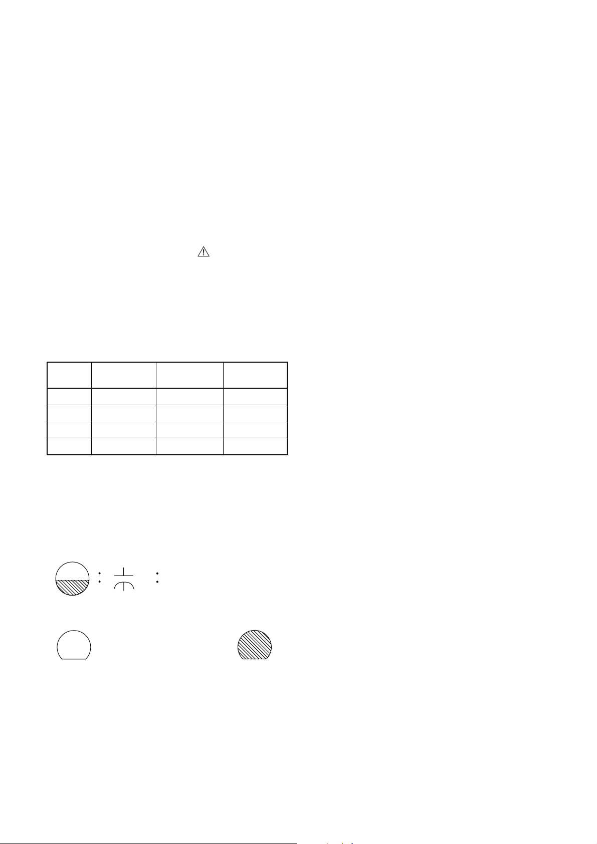
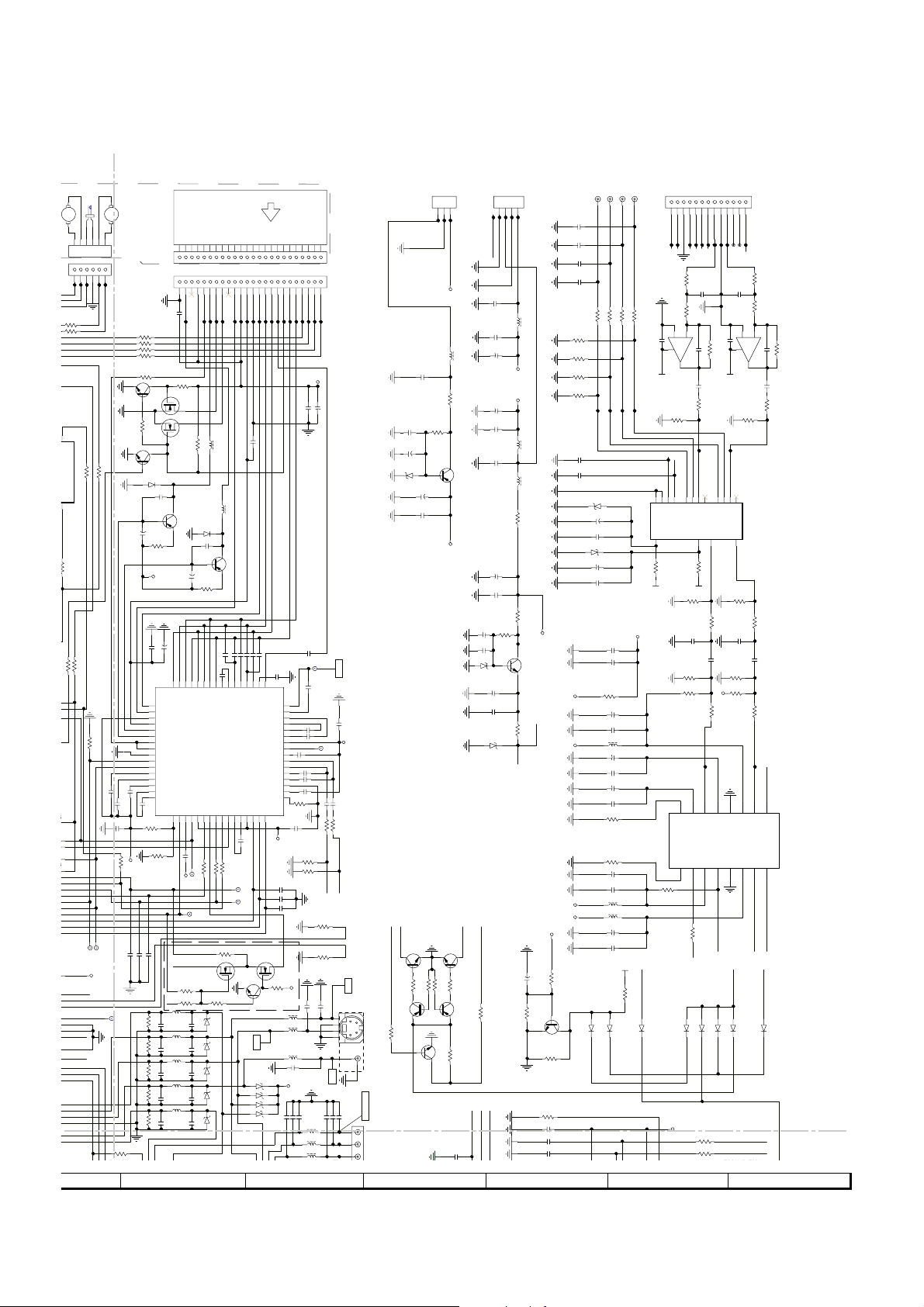
SCHEMATIC DIAGRAMS / IC’S PIN VOLTAGE
Standard Notes
WARNING
Many electrical and mechanical parts in this chassis
have special characteristics. These characteristics often
pass unnoticed and the protection afforded by them
cannot necessarily be obtained by using replacement
components rated for higher voltage, wattage, etc.
Replacement parts that have these special safety
characteristics are identified in this manual and its
supplements; electrical components having such
features are identified by the mark " " in the schematic
diagram and the parts list. Before replacing any of these
components, read the parts list in this manual carefully.
The use of substitute replacement parts that do not
have the same safety characteristics as specified in the
parts list may create shock, fire, or other hazards.
Capacitor Temperature Markings
Mark
(B)
(F)
(SR)
(Z)
Capacity
change rate
±10%
+30 - 80%
±15%
+30 - 80%
Standard
temperature
20°C
20°C
20°C
20°C
Temperature
range
-25~+85°C
-25~+85°C
-25~+85°C
-10~+70°C
Notes:
1. Do not use the part number shown on these drawings for ordering. The correct part number is shown
in the parts list, and may be slightly different or
amended since these drawings were prepared.
2. All resistance values are indicated in ohms (K=10
3. Resistor wattages are 1/4W or 1/6W unless other-
4. All capacitance values are indicated in µF
5. All voltages are DC voltages unless otherwise speci-
6. Electrical parts such as capacitors, connectors, di-
6
).
M=10
wise specified.
-6
(P=10
fied.
odes, IC's, transistors, resistors, switches, and fuses
are identified by four digits. The first two digits are
not shown for each component. In each block of the
diagram, there is a note such as shown below to
indicate these abbreviated two digits.
µF).
3
,
Capacitors and transistors are represented by the
following symbols.
CBA Symbols
(Top View) (Bottom View)
+
Electrolytic Capacitor
(Top View)
Transistor Transistor
ECB
(Top View)
ECB
16
Page 17

HT-CN410DVH
LIST OF CAUTION, NOTES, AND SYMBOLS USED IN THE SCHEMATIC DIAGRAMS
ON THE FOLLOWING PAGES:
1.CAUTION:
FOR CONTINUED PROTECTION AGAINST FIRE HAZARD, REPLACE ONLY WITH THE
SAME TYPE FUSE.
2.CAUTION:
Fixed Voltage (or Auto voltage selectable) power supply circuit is used in this unit.
If Main Fuse (F1001) is blown, first check to see that all components in the power supply circuit are not defective
before you connect the AC plug to the AC power supply. Otherwise it may cause some components in the power
supply circuit to fail.
3.Note:
(1)Do not use the part number shown on the drawings for ordering. The correct pa rt number is shown in the part s list,
and may be slightly different or amended since the drawings were prepared.
(2)To maintain original function and reliability of repaired units, use only original replacement parts which are listed
with their part numbers in the parts list section of the service manual.
17
Page 18
HT-CN410DVH
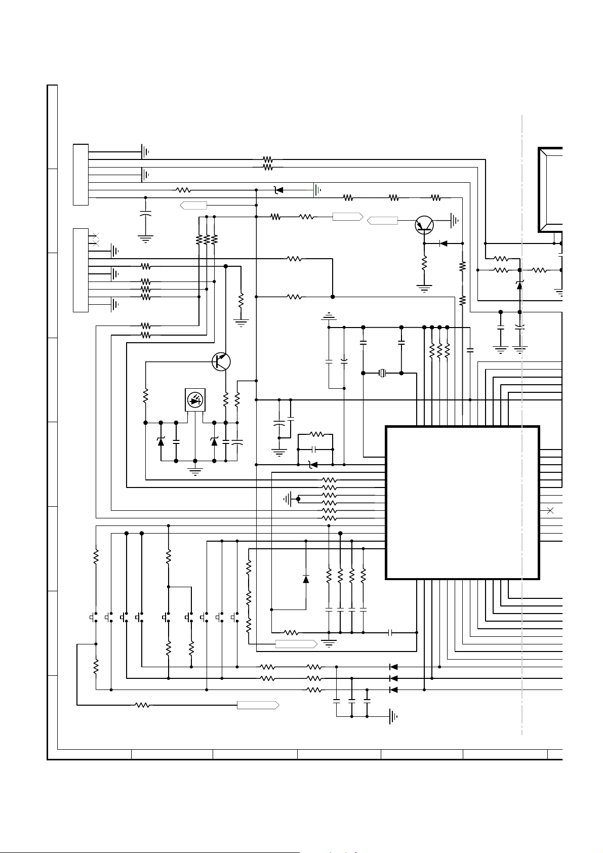
SCHEMATIC DIAGRAM FOR CONTROL PCB
A
RB5503
7
GND
6
AC1
5
AC2
4
GND
3
-27VF
2
BK5V
1
ON/OFF
B
RB204
10
9
8
7
6
5
4
3
C
2
1
CN10/20
R2532
R2533
R2534
R2535
R2558
R2559
R2564 10 ZD255 5V1
R25364.7K
R25374.7K
R25381.2K
BK5V
Q2502
2SC1623
+
C2520
100UF/16V
PMUTE
0
IR
0
VFD_DA
0
VFD_CK
0
VFD_CE
0
0
BK5V
D
SN251
SENSOR
R2504 47K
123
5V6
C2514 100P
E
ZD251
5V6
ZD252
VFD_DA
VFD_CK
VFD_CE
R2507 1K5
+
C2515 104
F
NEXT
TA2502
SOURCE
TA2503
0
R2548 0R2549 0
UP
STOP
PREV
TA2504
SELECT
TA2506
TA2505
R2546
DOWN
TA2509
TA2508
R2550 0
R2547
TA2507-2
TA2507-2
R2551 0
OPEN/CLOSE
PLAY/PAUSE
G
TA2510
0
R2553
TA2501
R2552
H
R2539
R2540
R2506 10K
R2505 47
C2504
100UF/16V
R2554 0 R2555 0
3.3K
R2542
0
0
R2556
0
R2528 1K
R2513 4K7
+
C2503
100UF/16V
R2529 10k
TA2507-1
TA2507-1
0
0
R2501
1K
104
C2511
R2541
C2521
ZD253
R2520 470
R2521 33
R2514 10K
R2515 10K
R2522 33
R2523 33
D2504 1N4148
R2543
R2544
R2545
LED-1
22k
104
3V
2.2K
2.2K
2.2K
R2502
R2516 10K
223
C2525
C2516 104
223
C2524
103
C2528
LED-1
10K
R2517
C2523 22 3
103
C2527
4.7K
C2505 10U/50V
10K
R2518
223
C2522
R2519 33K
103
C2526
R2560
0
LED-2
LED-2
150P
C2506
XL2501
455K
1
2
3
4
5
6
7
8
9
10
11
12
13
C2512 104
D2506 1N4148
D2507 1N4148
D2508 1N4148
C2507
OSC1*
RESET*
MODE*
REMOTE*
Din/out*
IIC SDA*
IIC SCL*
CLK
STB
K1
K2
K3
K4
R2563
Q2501
2SA812
D2501
1N4148
R2509 10K
150P
R2510 10K
50
51
52
GND
OSC2
GPIO1*
VDD14Seg1/KS1
Seg2/KS2
15
16
0
10K
10K
R2511
R2512
47
48
49
GPIO2*
GPIO3*
GPIO4*
IC251
V63111
Seg3/KS3
Seg4/KS4
Seg5/KS5
17
18
19
R2524 1K
0
R2525 1K R2526 22K
R2562
0
R2561
C2508 104
43
44
45
46
VDD
Grid1
Grid2
PSW*
Seg6/KS6
Seg7/KS7
Seg8/KS8
Seg9/KS9
20
21
22
23
C2509 104
40
41
42
Grid3
Grid4
Grid5
Grid6
Grid7
Grid8
Seg20/Grid9
Seg19/Grig10
VEE
VDD
Seg18/Grid11
Seg17/Grid12
Seg16/Grid13
Seg15/Grid14
Seg14/Grid15
Seg13/Grid16
Seg10/KS10
Seg11/KS11
Seg12/KS12
24
25
26
ZD254
5V6
C2513
DP251
220U/35V
39
38
37
36
35
34
33
32
31
30
29
28
27
1
2
1
23456
Figure 1: SCHEMATIC DIAGRAM FOR CONTROL PCB (1/2)
18
Page 19
HT-CN410DVH
Seg11/KS11
Grid4
DP251
DISPLAY
41K
51K R2526 22K
ZD254
5V6
C2513
220U/35V
40
Grid5
eg20/Grid9
g19/Grig10
g18/Grid11
g17/Grid12
g16/Grid13
g15/Grid14
g14/Grid15
g13/Grid16
Grid6
Grid7
Grid8
VEE
VDD
39
38
37
36
35
34
33
32
31
30
29
28
27
123456789
C2501
104
C2510
104
1011121314151617181920212223242526272829303132333435363738
JK5501
EARPHONE
39
C2502
104
JP2
EARPHONE SECTION
7
6
3
2
4
5
1
C5501
104
C5502
104
FB5505
FB5506
C5507
FB5507
104
JP3
600
600
600
RB5501
1
2
3
4
Seg12/KS12
26
6
CN5504
5
4
3
2
1
RB5504
CN5/20/Z
GND
TA2507-1
TA2507-2
LED-2
LED-1
TA2507-1
TA2507-2
LED-2
LED-1
CN5/20/Z
7
8 9 10 11 12
JP1
GND
5
4
3
2
1
LD2501
ZD262
TA2507
POWER
STANDBY
5V6
Figure 1: SCHEMATIC DIAGRAM FOR CONTROL PCB (2/2)
19
STANDBY SECTION
Page 20
HT-CN410DVH
1
1
3
5
B
S
B
5
SCHEMATIC DIAGRAM FOR POWER PCB
A
B
C
D
E
F
G
H
REMARKS :
R04 IS 1/4W
R06 IS 1/6W
!
!
F901
!
ECO POWER < 0.6W
R04-1-F IS 1/4W 1 OHMRES FUSE
R06-10KM IS 1/6W 10KOHM 1%
12
BD901
BD-KBU808
4
!
JMPAA
Jumper
12
43
L902
22mH
C904 0.22uF/275V
1000pF/250V
R04-910K
R901A
R04-910K
R901
L901
!
22mH
T3.15AL 250V
C905
C474P-275V
CN901
CN2P-396-2
12
C903
1
C906
1000pF/250V
43
2
3
!
!
GT901
R902
R04-220
RT-5A
NTC901
!
!
GT10
!
C907
100U 250V
C908
100U 250V
R912
567
3
FSDM0265RN
R915
R06-4.7K
PAD-D2.6
103P-1KV
C909
103P-1KV
C910
R920
R20-47
R04-220K
IC902
1
4
MC104P
P5
PAD-D2.6
SP1CREW-A
SP2CREW-A
R903
R04-470K
R904
R04-470K
222P-1KV
8
2
C918
22U 50V
C917
0.0022uF/400V
P6
0.0022uF/400V
R906R04-47
C915
!
C921
C922
C911
C155P-250V
R907
R905R04-47
R04-2K7
R908R04-2K7
R916
R06-10
C919
CC104P
ZD906
ZD-5V1
!
Q901
G
D903
1N4148
ZD901
ZD-15V
!
Q902
G
D904
1N4148
ZD902
ZD-15V
R914
R04-62K
D907
PR1507
D910 HER104
C926
221P-1KV
R919
R06-27
1000pF/250V
C923
1000pF/250V
C924
SP3CREW-A
SP4CREW-A
DS
STP9NK50Z
!
DS
STP9NK50Z
C916
C913
102P-1KV
R909
R30-120
C914
102P-1KV
R910
R30-120
!
5
T903
101P-1KV
3
2 9
IC901
IC-EL817C
3
P9
PAD-2.6
P10
PAD-2.6
C920
2
R917
6
7
8
220P-1KV
101
!
T901
3
470P-1KV
R30-120
6
4
5
1
2
1
24
P11
PAD-D2.6
P8
PAD-D2.6
P7
PAD-D2.6
!
5
T902
!
6
8
10
3
C983 220P-1KV
D959
D960
C981
220P-1KV
C982
220P-1KV
R980
R06-220
R06-1K5
R981
10
C951
14
15
C952
12
HER1 04
1N5822
C984
C992
CC104P
C966 MC104P
3
IC953
IC-TL4 31
470P-1KV
470P-1KV
Q951
Q952
2SA733
C104P-100V
C985
1000U 16V
2
C953
102P-1KV
R993
R10-120
C E
CE
470U 2
R982
R06-1K
R98
R06-4
2
1
C986
1
23456
Figure 2: SCHEMATIC DIAGRAM FOR POWER PCB (1/2)
20
Page 21
HT-CN410DVH
C951
9
10
470P-1KV
14
15
470P-1KV
12
Q951
Q952
2SA733
20P-1KV
R104
5822
C104P-100V
84
V
C985
1000U 16V
C992
CC104P
C966 MC104P
3
953
L431
2
C953
102P-1KV
R993
R10-120
2SA733
C E
CE
470U 25V
C986
R982
R06-1K5
R983
R06-4K7
470P-1KV
C955
FEP16DT
1
3
HER1 04
D952
L951
3
1
1N4148
D957
B
R973
B
D958
1N4148
C987
R985 R04-4R7-F
R986 R04-4R7-F
1
R974
L955
L-6uH-0.6A
L956
L-6uH-2A
C994
C104P-100V
R987
R06-5K1
C997
CC104P
D951
2
C956
470P-1KV
C959
470P-1KV
6
5
4
R06-560
R06-560
1000U 16V
C989
R06-30K
D954
1N4148
D961
1N4148
R971 R06-56
R972 R06-56
R977
R06-6K8
C990
R970
R06-1K
STP16NF06
D S
G
R997
R976
R06-10K
L952
1 2
4 3
C971
B
Q956
2SA952
CC104P
R996
R06-15K
L-10UH
R984
R06-27
Q953
R975
R06-1K
C961
1000U 50V
C962
1000U 50V
10U 50V
C974CC104P
R967
R989
R06-1K
CE
R978
R04-1-F
C988
470U 25V
L957
+5V
GND
123
R952
R06-5K6
R957
R06-10KM
R966
R06-4K7
2SC945
E C
C993
100U 16V
+12V6
GND
4
C104P-100V
C963
C964
C104P-100V
R06-30K
R951
R958
R06-100
C975
100U 16V
R06-3K9
Q959
B
CC104P
C967
ON/OFF
1234567
R959
R06-10KM
15
1
EA(-)
EA(+)
EA(-)2COM/INVERF
EA(+)
16
C976
CC104P
R06-1K
R990
R991
R06-10K
C998
100U 16V
-27V
GND
BK5V
Jumper
JMP30
R06-33K
R960
C973
47U 50V
13
14
OUT/C
D/C4C-T5R-T6GND7C1
3
R968
R06-1K2
AC3V4
AC3V5
GND
D955 1N4148
R961
11
12
VCC
IC-KA7500C
M102P-100V
C977
IC951B
5
+
6
-
ZD952 ZD-3V9
3
+
IC951A
2
-
R06-15K
10
E2
C2
IC952
R969
R06-12K
CC104P
R979
R06-10
7
IC-BA4558D
R953
R02-2K2
R954
R04-22K
R962
R06-1K2
IC-BA45 58D
9
E1
8
C978
C991
1
R963
R06-330
1N4148
47U 16V
+32V
GND
-27V
R964
D956
84
+
IC951C
-
IC-BA4558D
CN951
3
2
1
CN3P-396
R06-4K7
CN952
CN4P-25
7
8 9 10 11 12
CN953
CN7P-20
Figure 2: SCHEMATIC DIAGRAM FOR POWER PCB (2/2)
21
Page 22
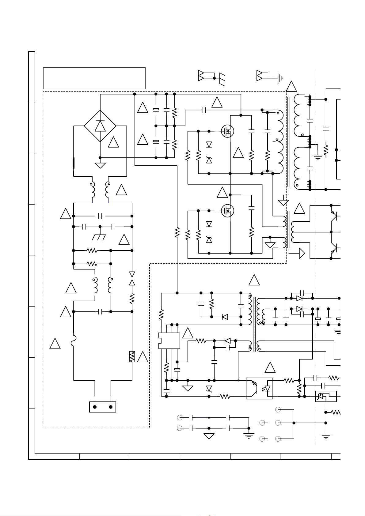
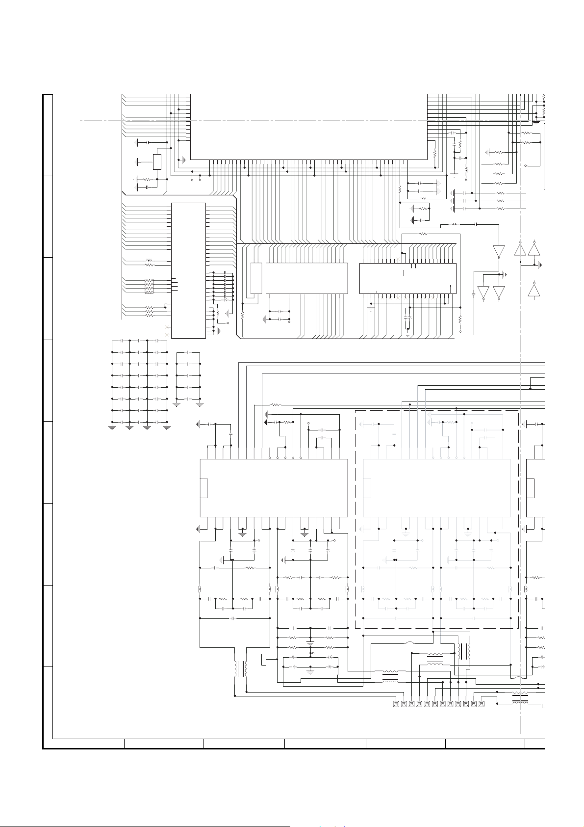
HT-CN410DVH
R850100K
C8 6
C849
2
C
2
5
5
6
6
6
6
6
6
6
7
7
7
7
7
7
8
8
8
8
8
8
8
8
9
9
9
1
1
1
1
MAIN CIRCUIT DIAGRAM
TP223
FB225 600
VFD_DA
D203
1N4001
R218 4K7
176
CN204
8
TP225
TP226
PMUTE
FB224 600 IR
R817 0
OPEN
D202
1N4001
D204
CLOSE
+5V
R838 1K
R839
+5V
1K
TP810
TP811
220U/10V
C809104
M
12345
CN802
12345
TP812
TP813
TP814
R811 0
R812 0
R813 0
R814 0
+5V
C845
FB803100
REGO2
REGO1
V33b
14
VOLD+
VOTK+
VOLD-
VOTK-
VCTL
OPIN
Vcc2
21
20
19
18
17
16
15
VINFC1TRB_ 12REGO23VINSL+4REGO15FWD6REV7Vcc18VOTR-9VOTR+10VOSL+11VOSL-12VOFC-13VOFC+
OPOUT
TRB_ 2
VINTK
VINLD
MUTE
BIAS
GND
27
26
25
24
23
22
V18b
R844 5K6
R846 10K
R827 4K7
R2042 4 K7
158
159
160
161
162
163
SLV
DMO
FOO
SLO
RPBC
FLAG/AUX30/CAMIN0
FLAG/AUX35/CAMIN5
TXD0/AUX14/PWM_O4R
TXD0/AUX15/PWM_O4L
TBCK/PWM_O1R
TSD3/PWM_O3R
TSD2/PWM_O3L
TSD/PWM_O2R/PLL1
TSD/PWM_O2L/PLL0
TWS/PWM_O1L/PLL2
SPD_DOBM/PLL3
SPDIF
R849 1M
R264 1K
R265 1K2
R266
LDIN
C2005
10U/50V
C204
104
C205 104
157
AVSS
AVDD3
VREFIN
VREFOUT
RFENV
BSUM
LDON
XSCEI
LDCO
RXD1/AUX12
TXD1/AUX13
MCLK
ADC_CAP
ADC_BIAS
UDAC
CDAC
YDAC
VS33_DAC
VD33_DAC
VDAC
FDAC
COMP
VS33_PLL
VD33PLL
R80475K
D804 IN4148
C254
C266 474
C255
1K
156
155
154
153
152
TE
151
CE
150
FE
149
148
147
MIRR
146
DFCT
145
SCLK
144
143
SDEN
142
IP2
141
LG
140
139
RX
138
VSS
137
TX
136
135
134
VDD
133
VSS
132
131
130
VD33
129
128
127
126
125
124
123
VSS
122
VD33
121
120
119
118
117
MIC
116
115
114
113
112
111
110
109
108
RSET
107
106
VREF
105
IC201
103
103
R267 1K2
R215 4K7
AUX30
AUX35
C2009104
R286 0
C817
100U/16V
C810 104
C2006
10U/50V
C206
C207
C2008
R864 0
BPWM4R
BPWM4L
BPWM1R
BPWM3L
BPWM2R
BPWM2L
BPWM1L
C2010
104
C811
104
C846
474
VD33
104
104
105
R249 4K7
R250 4K7
R273
R259 4K7
R248 33
U0
V0
Y0
R285 390
FB
R852
47K
R81 5 3 3
R81 6
3K
VD33
L209 1UH
C2007 682
R239 0
OPEN
R208
R278 39K
R205 0
RA201 33
R240 4K7
CS5342RESET
33
VD33
VCC18
INTR
L210 1UH
C2014 100U/16V
C221 104
TP216
INB
IN
TEBC
164
165
166
167IN168
169
170
171
172
173
174
175
DVCC
IP1
IDSEL
AMPSTBY
FGIN
LCS3 #
LD[7]9LD[6]9LD[5]9LD[4]9LD[3]9LD[2]
VDD
VSS
TRO
TESTDA
TEBC
REFD
INB
AVDD3
AVSS
VD33
LD[1]9LD[0]9LOE#1LA[1]
VSS
M
TP815
28
R848
22K
R2424K7
R272 33
M
12345
6
CN803
12345
6
TP818
TP819
TP816
TP817
R854
R855
R856
R857
R862
2SC2812
2SC2812
Q806
R835 33K
R851 4K3
IC802 AM5869S
D802
R82 8 4K 7
R80 5 10 K
100U/16V
R830 4K7
C834 822
C848 822
C847
150P
224
C812
104
R8
R276
RF5V
0
LDON
C820
MIRR
330P
102
VD33
MCLK
R279
75
R280
75
R281
75
R282
75
R283
75
MCLK
BCLK
TSD2
C841
R2454K7
R2464K7
JK204B
R222 4K7
R224 4K7
R225
R226
R227
R228 4K7
C2016 27P
FB216 OPEN
C2017
C2019 27P
C2020 100P
C2021 100P
C2022
C2023
R294 33 0
195
196
197
198
CLK
VSS
VD33
FLAG[4]/AUX34
LA[10 ]
LA[20 ]6LA[21 ]
VD33
LA[9]
4
5
C292
100P
TP231
FB215 2.7 UH
C276
100P
R292
100
R293 330
R229
0
SPDI F-OUT
REGO2
12K
R2003
R2004
R2006
12K
10K
REGO1C2002
TU_DA
TU_CE
TU_CK
EN1
TU_DO
4K7
4K7
4K7
27P
100P
100P
RA2 04 33
AUX3
187
188
189
190
191
192
193
194
EAUX01
FEAG[6 ]/AUX36
EAUX00
EAUX03
EAUX02
VSYNC/AUX17
HSYNC/AUX16
VID_XI
VID_XO
ESS6809
LWRLL#
LA[19 ]6LA[18 ]
LA[8]
LA[7]7LA[6]7LA[5]7LA[4]7LA[3]
VDD
VSS
C2004
470U/10V
C242 104
7K5
R2002
R2005
C232 104
470U/10V
EN2
185
186
AUX[7]
FLAG[7]/AUX37/CAMIN7
C285 27P
C286 27P
C287 27P
C288 27P
C289 27P
10K
VFD_CK
RA2 03 33
183
184
VD33
VSS
VSS
VCC18 VD3 3
181
182
MDET
VD33
1234567
TP221
FB227 600
VFD_CE
V18b V33b
2SA952
2SB772
R220 4K7
178
179
180
CLOSE
OPENSW
OPEN
LA[17 ]
LA[2]
LA[0]
TP222
FB226 600
VFD_CK
Q205
Q206
177
HOMESW
LCS0 #8LCS1 #8LCS2 #
1N4001
CLOSESW
M1 M2 M3 M4 M5 M6 M7
C224 104
C225 104
A
B
C226
C227
C228 104
C229 104
C230 104
C231 104
M8
C233 104
C234 104
SMT MARK A SMT MARK B
C235 104
C236 104
C237 104
C238
C239
C240
TP1 TP2 TP3 TP4
C241
C243
VD33
104
104
VCC18
104
104
104
104
104
10U/50V
C2045
C2046
104
220U/10V
C2003
C217
104
+5V
FB218 100
220U/10V
C299
C223
104
MVCC
220U/10V
C295
C220
104
220U/10V
C296
C218
104
FB220 100
VCCV
L213 10uH
RF5V
VD33
L215 10uH
D5V
VD33
L212 10uH
RF3V3
FB229 100
SCART3
4052A
4052B
Q02Q15Q26Q39Q412Q515Q616Q719VCC20GND
LD0
LD1
LD2
C2026
C2027 27P
C2028
C2029 27P
C2030 27P
R251 33
R297 5K6
27P
27P
RA205 33
ESS6826
10
11
12
13
14
15
16
17
18
19
20
21
22
23
24
25
26
27
28
29
30
31
32
33
34
35
36
37
38
39
40
41
42
43
44
45
46
47
48
49
50
51
52
C283
100U/10V
C284
VFD_CE
VFD_DA
1
VD33
2
AUX[O]
3
AUX[3]
4
RESET#
5
AUX[1]
6
DMA[4]
7
DMA[5]
8
DMA[6]
9
DMA[7]
VSS
VD33
DMA[8]
DMA[9]
DMA[3]
DMA[2]
DMA[1]
DMA[0]
DMA[10]
VSS
VD33
DMA[11]
DRAS2#
DRAS1#
DCS1#
DCS0#
DRAS0#
VSS
VDD
DCAS#
DOE#
DWE#
DSCK
DQM
DB[7]
VSS
VD33
DB[6]
DB[5]
DB[4]
DB[3]
DB[2]
DB[1]
DB[0]
VSS
VD33
DB[8]
DB[9]
DB[10]
DB[11]
DB[12]
DB[13]
VSS
IR
C
R20 08
10K
SMUTE
MVCC
SCART2
SCART1
MUTE
R2007 10K
L211
IuH
C24 4
104
D
E
F
G
H
10
CLK
OE
1
11D718D617D514D413D38D27D14D03
LCS1#
C2043
OPEN
SDA
SCL
AT24C02
C2032
C2033 100P
R268 1K
DMA[4]
DMA[5]
DMA[6]
DMA[7]
RA210 10
RA211 10
DMA[8]
DMA[9]
DMA[3]
DMA[2]
DMA[1]
DMA[0]
DMA[10]
DMA[11]
DRAS2#
DRAS1#
DCS0#
DRAS0#
DCAS#
DOE#
DWE#
DSCK
DQM
DB7
DB6
DB5
DB4
DB3
DB2
DB1
DB0
DB8
DB9
DB10
DB11
DB12
DB13
C279
LM809
IC209 74HC374
LD3
LD4
LD5
LD6
LD7
4
VD33
S01S12S23GND
IC203
VCC
SDA
SCL
5
6WC7
8
R298 5K6
100P
RA21210
33
R252
104
IC204
3
213456
VCC
1
C297
100U/10V
C219
DVCC
EARP/W
RDDA
VSS
VD33
ST_LED
TU_LED
R232 4K7
R233 4K7
R234 OPEN
R235 4K7
R236
R269
R270 4k7
C2024 27P
206
207
208
AUX[4]
AUX[6]
AUX[2]
DB[14]5DB[15]
LA[16 ]5LA[15 ]5LA[14 ]5LA[13 ]5LA[12 ]6LA[11 ]
104
VD33
VD33
4K7
4k7
C2025 27P
102
C253
27MHZ
XL201
R277
100K
RA206
33
199
200
201
202
203
204
205
FLAG[1]/AUX31
FLAG[3]/AUX33
VSS
VDD
FLAG[2]/AUX32
AUX[5]
VSS
104
RD_CK
Figure 3: MAIN CIRCUIT DIAGRAM (1/4)
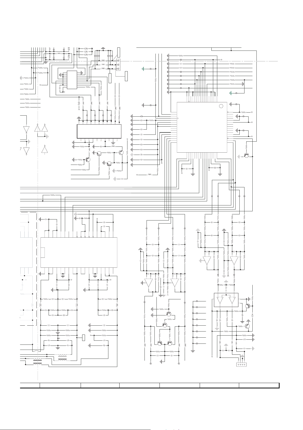
22
Page 23
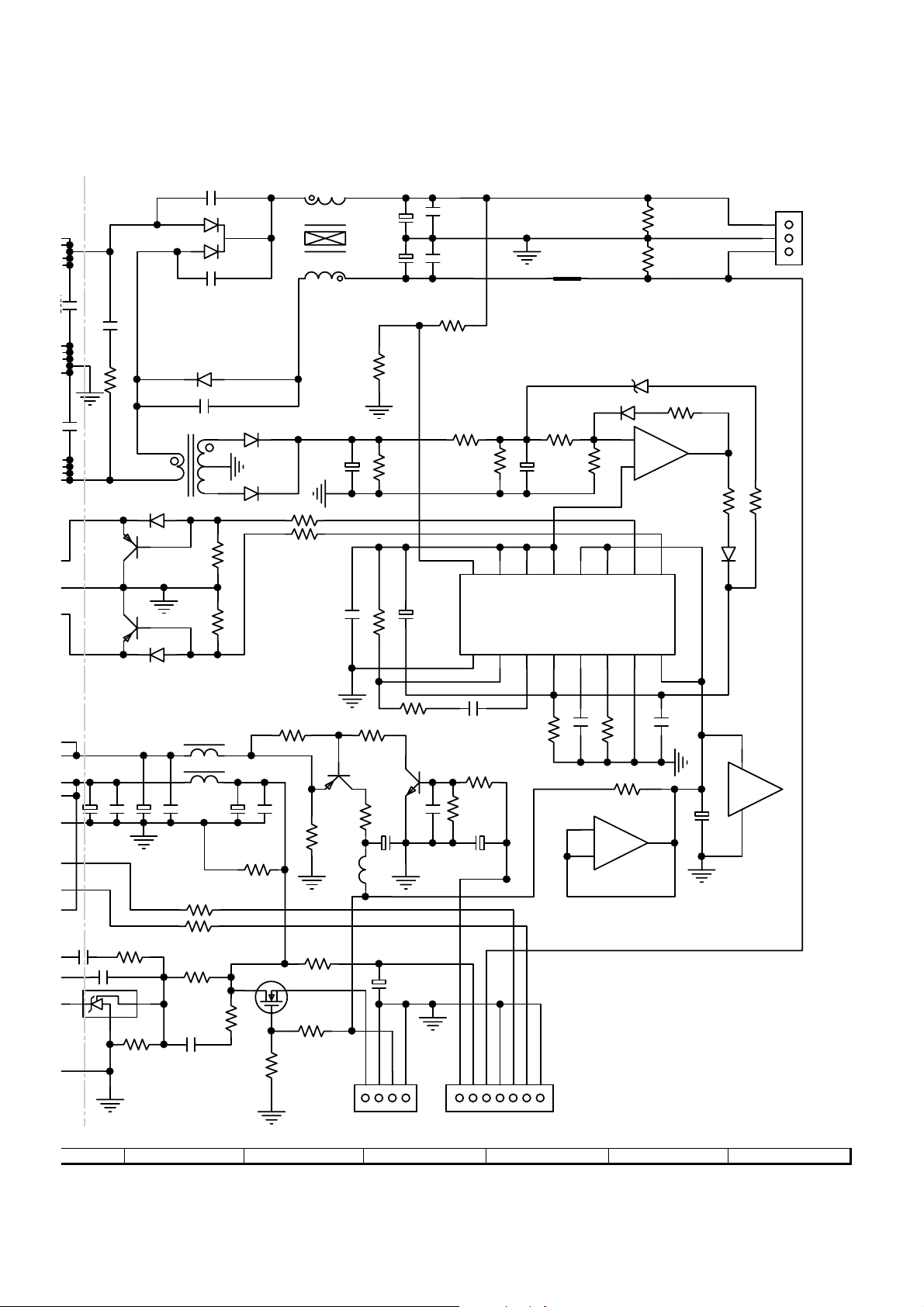
HT-CN410DVH
M
TP815
1
28
R848
22K
R80 5 10 K
2
EN
9K
0
4K7
5342RESET
K7
K7
BCLK
K7
TSD2
R2424K7
DVD_24PIN
M
12345
6
CN803
12345
6
TP818
TP819
TP816
TP817
0
0
R854 0
R855 0
R856 0
R857 0
R862 0
2SC2812
2SC2812
Q806
R835 33K
R851 4K3
IC802 AM5869S
D802
100U/16V
DVDLDO
VR_DVD
CDLDO
CDMDI
VR_CD
RF50V
GND
NC
NC
E
CD_DVD
TRACK +
TRACK -
FOCUS-
FOCUS+
DVD-B
DVDRF
DVD-A
RF50V
PCV
DVD-C
DVD-D
GND
F
CN801
24
VR_DVD
CDLDO
CDMDI
RF5V
DVDLDO
GND
C801104
TP835
TP836
TP837
TP838
TP839
Q801
2SK3018
18K
R801
Q805
R850100K
C81 6
2SK3018
1N4148
102
10
RF5V
R802 10K
Q803 2SB1132
100U/16V
D801
1N4148
C815
FB801 10 0
FB802 100
Q804 2SB1132
C818
102
Q802
C819
R80 6
DVDRF-A
DVD-BFGND
PCV
RF5VEVR_CD
TP828
TP829
TP830
TP831
TP832
TP833
TP834
C803 104
1234567891011121314151617181920212223
FOCUS+
FOCUS-
TRACK+
TRACK-
DVD-C
DVD-D
CD_DV D
DVD
TP824
TP825
TP826
TP827
TP820
TP821
TP822
TP823
RF5V
C80 2 104
C814 100U/16V
C902 104
C903 104
C904
10U/16V
ZD5501
12V6
C905
C906
TP901
2K2
220U/16V
104
CN901
123
TP902
TP903
+30V
FB901 100
R901
100 1/2W
R902
Q901 2SB772
-12V
R80710
10U/16V
C821 104
R82 8 4K 7
C822 47U/16V
100P
16
17
CD_F
18
CD_E
19
VPB
20
R830 4K7
C834 822
C812
VC
21
DVDLD
22
CDLD
23
DVDPD
24
CDPD
25
VNB
26
LDON
27
MIRR
28
MP
29
MB
30
MLPF
C848 822
31
MIN
C847
150P
32
MEVO
C849
224
4K7
104
R829
R276
R825
4K7
RF5V
0
ESS6602
V125
LINK
V25
TPH35DFT
37
36
34
33
R834
C808
104
B
0
RF5V
DFT
C840 330P
C841
C820
MIRR
MCLK
LDON
330P
102
VD33
MCLK
R279
470P
75
R280
470P
75
R281
470P
75
R282
470P
75
R283
470P
75
TEBC
R865 5K1
AUX3
2.4UH
C257
2.4UH
C258
2.4UH
C260
2.4UH
C262
2.4UH
C265
R868 3K3
2SK3018
R867 4K7
5K1
R866
ZD205
L201
C256
470P
7V5
ZD206
L202
7V5
470P
C259
ZD207
L203
7V5
470P
C261
ZD208
L204
7V5
470P
C263
ZD209
L205
C264
470P
7V5
R2454K7
R2464K7
9
10
S2C
11
S1C
7
12
DD
13
C852 680P
R832 0
MNTR
R831 OPE N
GND8DC
DB
S2B
S1B
C826
C823 680P
OP
C829
LCN
44
43
42CE41FE40TE39PI38
TE
FE
Q809
ZD202 7V5
ZD203 7V5
ZD204 7V5
7
6
5
4
C825 OP
C824 680P
SCLK
V3345LCP
46
C839 47 3
WF2
ZD2017V5
C851 680P
SDATA
47
2SC2812
C804103
DVDFRP1DVDRFN2A23B24C25D26CP7CN8D9C10B11A12CD_D13CD_C14CD_B15CD_A
RFDC
RFSIN
ATOP
ATON
AIN
VPA
RFAC
BYP
DIN
FNP
FNN
VNA
MEV
SDEN
48
C842 33P
C843 33P
C844 33P
4K7
Q807
R870
FB205
64
63
62
61
60
59
AIP
58
57
56
55
54
DIP
53
52
51
50
49
RX
IC801
C807
RF3V3
2SK3018
Q808
FB204 120
FB206 120
C278 15P
VCCV
C274 470P
C827 680
C831
C832
C806
104
C835
C836
C833 103
R808
12K
104
4K7
4K7
RF5V
120
C272 470P
C273 470P
FB201 120
FB202 120
FB203 120
RF
C830 820P
104
104
104
104
C838 104
R810
0
R824
R826
R213 4K7
R214
C271 15P
TP246
TP245
TP802
C270 15P
WF12
C805 104
RF5V
C837 104
R809 0
INB
IN
LMuteON
HMute off
SMUTE
SCART_R
KTC3875
SVIDEO+VIDEO
6
WF8/WF9
JK_RCA _YUV
JK202
JK201
Q404
R411 10K
R409 1K
2SA733
Q406
R414 10K
SCART_MUTE
4K7
WF3
1
2
3
4
5
WF1
C267 15P
C268 15P
C269 15P
V
1
TP232
U
3
TP233
Y
5
TP234
C915
104
ZD902
C282
ZD903OPEN
SCART_L
KTC3875
R410 10K
R408 1K
Q403
2SA733
Q405
R412
Q407
2SC1623
6K8
MCLK
ESS129P
C577
15P
R502
8 9 10 11 12
TP904
BK5V
C909 104
C910 104
C911
470U/10V
C912
470U/16V
C913 104
C914 104
C908
220U/16V
C907
C901
5V6
100U/16V
C916
+12V
R413 10K
SDA
SCL
ESS2P
ESS5P
CN9 02
123
4
TP905
TP906
TP907
TP908
C301 100P
GND
GND
+P5V
+P12V
C302 100P
C303
C304
100P
100P
FB902 100
R305
47K
R306
47K
R307
TU12 V+5V
FB903
33 ohm
FB904 100
R903 0
47K
R308
47K
C313
C312 104
ZD302
C324
C314
ZD301
C323
104
R904
R905
2K2
101/4W
C311
+12V
Q902 2SC1623
AD5V
104
OPEN
R906
AD5V
VD33
DAVCC
VD33
JK401F
JK401E
TV-L
TV-R
TP404
R304
12K
TV_L
TV_R
TRIN
104
5V6
47U/16V
104
5V6
47U/16V
104
104
100U/16V
R317 0
C325
C326
FB301 10R
C327
C328
C329
C330
R333 10K
JK401C
TP403
R303
12K
TLIN
C335
10U/16V
10U/16V
AUX-R
TP402
R302
12K
AUX_R
ARIN
C336
100U/16V
104
104
104
JK401D
AUX-L
TP401
R301
12K
AUX_L
ALIN
DAVCC
TU_DA
TU_CK
RDDA
RD_CK
TU_DO
TP310
TP308
TP309
TP311
TP312
TUN_R
R338 10K
C306 102
R310 10 K
C310 104
6
C316 47 P
+5-
8
B+
JRC4558
IC301B
7
+12V
C318
4.7U
R319
8K2
TU_R
R312 10K
TURIN
4052A
4052B
AUX_R
TV_R
TU-R
8
VDD
VEE
7
16
R324 330
-12V
R323 330
+12V
100K
R321
680
C321
470P
4.7U
VA33
150
12
16
FILT+15MI
IC303 CS5342
R335 10K
D403 1N4148
MCLK
M0
1
2VL3
R336
100
MCLK
D412 1N4148
LIN_MUTE
VD33
R512 0
R511 0
R510 0
R506 220
R509 33
D402 1N4148
47U/16V
220K
AMP_MUTE
R501 0
C506 104
C508 15P
C507 15P
C505 15P
C504 47P
R332 10K
C331
100U/16V
104
C332
DAVCCDAVCC
FB302 10R
FB303 10R
+5V
C333
100U/16V
104
C334
LIN_MUTE
D414 1N4148
H-MUTE
D407 1N4148
+12V
ESS204P
EARP/W
R401
10K
R403 47K
C401
2SC1623
Q401
R405
CONTRO L_MUTE
8K2
R406
TUN-R
TU_CE
TP306
TP307
R315 15K
TV_L
Y-COM3X-COM
ROUT
R313
C319
VA33
R329
ADRIN
VQ11AINR
SDOUT
4
DOUT
H-MUTE
TUN-L
GND
TU12V
ST_LED
TP302
TP303
TP304
TP305
TUN_L
C305 102
C309 104
+3-
4
JRC455 8
IC301A
-12V
R31110K
TULIN
TU-L
AUX_L
X012X114X215X311Y01Y15Y22Y34B9A10INH6VSS
13
LOUT
R322
100K
C322
470P
R326 100KR325 100K
R328 100KR327100K
VA13AGND14RST
DGND
5VD6
ADOUT
KEY
PMUTE
D409 IN4148
D406 1N4148
ESS124P
ESS121P
ESS120P
ESS126P BCLK
12345678910111213
TU_LED
TP301
B-
1
TC4052B
680
4.7U
150
TSD2
TSD1
TSD0
LRCLKESS119P
CN301
R
10K
R309
10K
R316 15K
C315 47P
2
C317
4.7U
R320
8K2
TU_L
IC302
R314
C320
R330
ADLIN
CS5342RESET
10
9
AINL
LRCK
SCLK
7
8
BLCK
LRCK
ESS 94P
MUTE H-MUT E
D405 1N4148
Figure 3: MAIN CIRCUIT DIAGRAM (2/4)
23
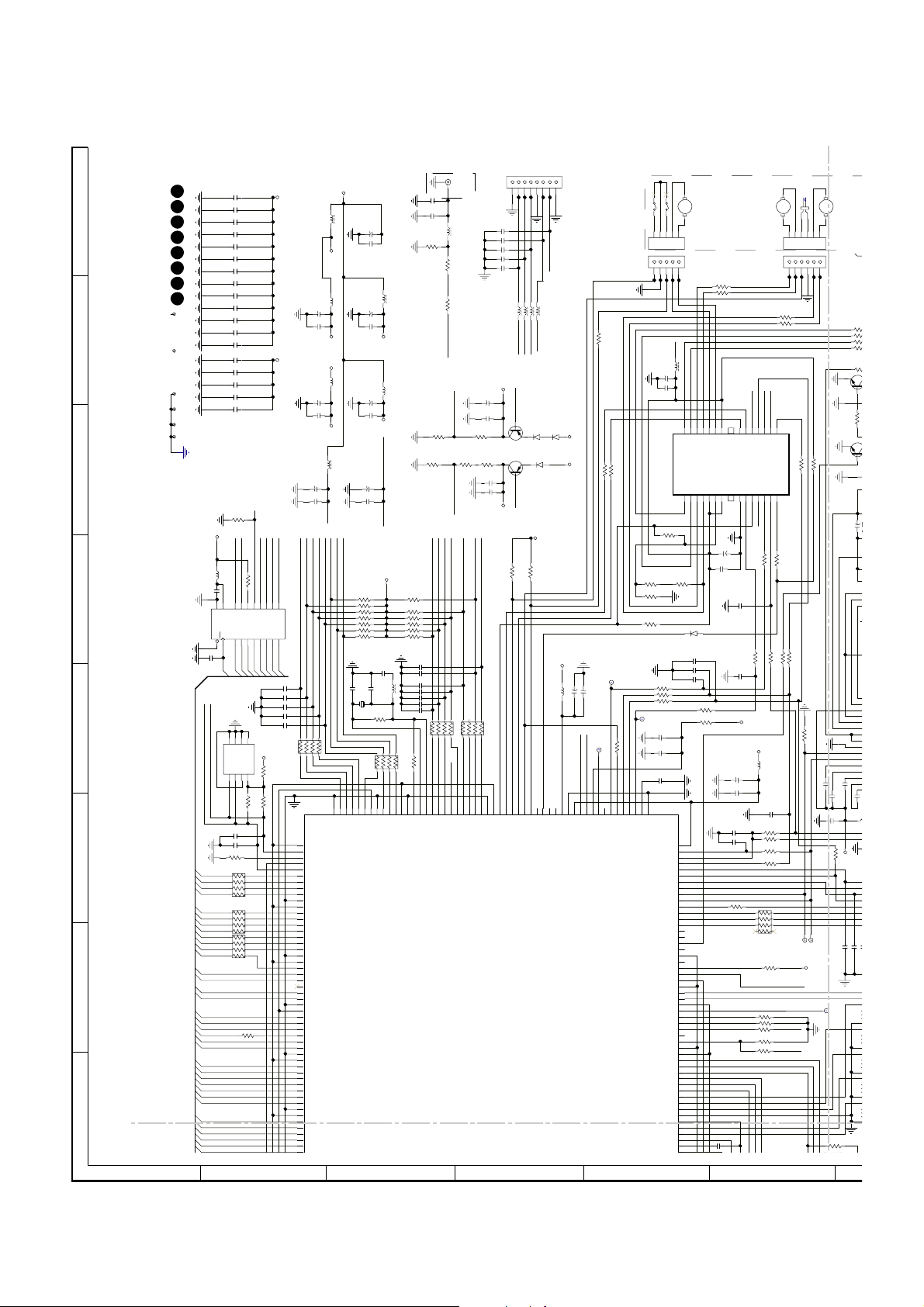
Page 24
HT-CN410DVH
3
C
2
3
/
R
DB[3]
MIC
5
A
B
C
D
E
75
R2454K7
R2464K7
VD33
DOUT
BLCK
LRCK
65
IC205C74HC04
UN-BTL DELET E
STA518
IC503
282
R283
75
43
IC205B74HC04
IC205A 74HC04
21
R523
C527
104
36
VSIG35VSIG
DB2
DB1
DB0
DB8
DB9
DB10
DB11
DB12
DB13
104
C279
LM809
IC204
VCC
1
RES
R204
10K
104
C245
DMA[0]
DMA[1]
DMA[2]
DMA[3]
DMA[4]
DMA[5]
DMA[6]
DMA[7]
DMA[8]
DMA[9]
DMA[10]
DMA[11]
DSCK
FB217 60R
DOE#
R25333
DCS0#
45
DRAS0#
3
6
DCAS#
2
7
DWE#
1
8
RA207
33
R25433
DQM
DRAS1#
33
R255
DRAS2#
33
R256
C101
104
C109
104
C117
104
C102
104
C110
104
C118
104
C103
104
C111
104
C119
104
C104
104
C112
104
C120
104
C105
104
C113
104
C121
104
C106
104
C114
104
C122
104
C107
104
C115
104
C123
104
C108
104
C116
104
C124
104
41
DB[2]
42
DB[1]
43
DB[0]
44
VSS
45
VD33
46
DB[8]
47
DB[9]
48
DB[10]
49
DB[11]
50
DB[12]
51
DB[13]
52
VSS
ESS6826
DB[14]54DB[15]
3
2
RESET
23
A0
24
A1
25
A2
26
A3
29
A4
30
A5
31
A6
32
A7
33
A8
34
A9
22
A10
35
IC20 8 SDR AM_K4S641632
A11
38
CLK
37
CKE
19
CS
18
RAS
17
CAS
16
WE
15
DQML
39
DQMH
20
BA0
21
BA1
36
NC
40
NC
C125
104
C126
104
C127
104
C128
104
C129
104
LA[16 ]56LA[15 ]57LA[14 ]58LA[13 ]59LA[12 ]60LA[11 ]
VD33
53
DB14
VCC18
VD33
2
DQ0
4
DQ1
5
DQ2
7
DQ3
8
DQ4
10
DQ5
11
DQ6
13
DQ7
42
DQ8
44
DQ9
45
DQ10
47
DQ11
48
DQ12
50
DQ13
51
DQ14
53
DQ15
C246 104
1
VCC
C247 104
14
VCC
C248 104
27
VCC
C249 104
C250 104
3
VCCQ
C251 104
9
VCCQ
C252 104
43
VCCQ
49
VCCQ
6
VSSQ
12
VSSQ
4
VSSQ
52
VSSQ
28
VSS
41
VSS
54
VSS
C552
104
36
STA518
55
DB15
DB0
DB1
DB2
DB3
DB4
DB5
DB6
DB7
DB8
DB9
DB10
DB11
DB12
DB13
DB14
DB15
47U/16V
10uH
LA16
C2044
L214
VD33
VSS
61
62
63
LA12
LA13
LA14
LA15
LA11
LA20
LA21
R212 OPE N
VD33
LCS2#
SUB-
SUB+
C551 104
PWM2L
BPWM2 LB
LWRLL#
LA[10 ]
LA[20 ]66LA[21 ]
LA[19 ]69LA[18 ]
LA[9]
64
65
67
68
70
WRLL#
LA18
LA19
LA21
LA20
LA9
LA10
RESET
WRLL#
LA18
LA19
1
3
RESET1WE
CN202 OPEN
ADDR
GND
CLK
4
2
16
C222 104
C298
220U/10V
C
R521
0
FL
C550
104
PWM3L
BPWM3 LB
ESS6809
LA[17 ]
LCS0 #84LCS1 #85LCS2 #
VDD
72
LA15
10K
LA[7]74LA[6]75LA[5]76LA[4]77LA[3]
73
LA7
LA14
VCC
32
MVCC
R516
VD33
LA[2]
LA[0]
VSS
78
79
80
81
82
83
LA0
LA2
LA17
LA3
LA4
LA5
LA6
LA4
LA5
LA6
LA7
LA8
LA9
LA10
LA11
LA12
LA13
24
LOE#
LCS3#
LD4
LD5
LD6
LD7
VD33
C548
104
C549
104
LA[8]
VSS
71
LA8
LA16
LA17
IC206 IC_27C080-90(OPEN)
SPD_DOBM/PLL3
LCS3 #
VDD
VSS
86
87
88
LCS1#
LCS2#
LA0
LA1
LA2
LA3
A012A111A210A39A48A57A66A75A827A926A1023A1125A124A1328A1429A153A162A1730A1831A19
D013D114D215D317D418D519D620D721CE22OE
LD0
LD1
LD2
LD3
IC504
GNDREF19GNDR120VREG121VREG122VL23CONFIG24PWRDN25TRI-STATE26FAULT27TWARN28INLA29INLB30INRA31INRB32VREG233VREG234VSIG35VSIG
LD[7]90LD[6]91LD[5]92LD[4]93LD[3]94LD[2]
89
LCS3#
LD6
LD7
No use
OPT.
LD5
LD4
LD3
LA2
LA3
LA4
24
GND
A0
25E26
27G28
LA1
LCS3#
OPT.
36
VD33
LD[1]98LD[0]99LOE#
LA[1]
VSS
95
96
97
100
LOE#
LD2
LD1
LD0
LA5
LA6
LA7
LA8
LA18
LA19
IC207 MX26LV800BTC
DQ029DQ830DQ131DQ932DQ2
33
LD0
LD1
LD2
LOE#
C547
101
LA1
DQ10
34
C546 OPT .
VS33_DAC
VD33_DAC
VD33PLL
SPDIF
103
104
102
R202
C2013 100U/16V
C208 104
680
FB221 100
RESET
DQ11
VCC
DQ3
35
36
37
C294 220U/10V
C211 104
LD3
FL+
FL-
PWM1L
BPWM1 LB
ADC_BIAS
UDAC
CDAC
YDAC
VDAC
FDAC
RSET
COMP
VREF
VS33_PLL
R2174K7
C216
0
WRLL#
LA21
DQ12
DQ4
38
39
LD4
SL-
BPWM2 RB
116
115
114
113
112
111
110
109
108
107
106
105
IC201
47P
R20 6
LA9
LA10
LA20
DQ13
DQ14
DQ5
DQ6
40
41
42
U0
V0
Y0
C2009104
R285 390
C2010
R286 0
104
C2011
104
C209 33P
C210 33P
C212 33P
OOhm
L206
LA11
LA12
LA13
LA14
LA15
LA16 LA17
A151A142A133A124A115A106A97A88NC9NC10W11RP12VPP13DU/WP14NC15A1816A1717A718A619A520A421A322A223A1
DQ15/A_1
BYTE
GND
DQ7
A16
43
44
45
46
47
48
FB219 100
VD33
C203 104
C215
104
LRCLK
TSD0
TSD1
IC205E 74HC04
1011
R2424K7
R272 33
R274 33
R275 33
R231 33
R230 33
R241 180
IC205F 74HC04
1213
IC205D 74HC04
89
R207 0
LA0
LD5
LD6
LD7
SL+
C545
OPT.
PWM2R
SPDI F-OUT
VD33
VD33
C543
R515
OPT.
OPT.
C544
OPT.
GNDREF19GNDR120VREG121VREG122VL23CONFIG24PWRDN25TRI-STATE26FAULT27TWARN28INLA29INLB30INRA31INRB32VREG233VREG234VSIG35VSIG
STA518 DIGITAL POWER STA518 DIGITAL POWER
PGND2N
4
104/100V
C54 2
R522A 20
6R2
R534A
104/50V
C581A
C588A 824/63V
5
6R2
R533A
104/50V
C580A
PGND2P
VCC2P7OUTPR8OUTPR9OUTNL10OUTNL
6
+30V
1U/50V
C53 6
30UH/2A
104/50V
C579A
SUB+
OUTNR2OUTNR3VCC2N
GNDS
1
F
C558A 330/50V
L512
30UH/2A
104/50V
C582A
SUB-
G
WF10
31
L518
20uH
24
TP511
TP512
H
213456
Figure 3: MAIN CIRCUIT DIAGRAM (3/4)
PGND1N
PGND1P
VCC1N
VCC1P
OUTPL16OUTPL
11
12
13
14
15
17NC18
+30V
1000U/50V
104/100V
1U/50V
C53 5
C541
C530
30UH/2A
R504B
L510
L511
104/50V
C578A
C503B
C504B
330/50V
20
6R2
R532A
104/50V
C577A
330/50V
R531A
104/50V
C576A
R503B
20
6R2
104/50V
C575A
GNDS
C556A OPT.
30UH/2A
L508
OPT.
L509
C574A
OPT.
FL-
C556B 824/63VC557B 824/63V
R541B 3K3R543B 3K3
+30V
C-
(FL+)
(FL-)
C567B
220U/35V
R542B 3K3R544B 3K3
220U/35VC566B 2C564B20U/35V
C565B
220U/35V
C+
(C+)
(C-)
OUTNR2OUTNR3VCC2N
1
OPT.
OPT.
R530A
OPT.
C573A
C586A OPT.
JP501B
L515 20uH
31
+SUB
6CH
PGND2N
PGND2P
4
5
6
OPT.
C540
R520A OPT.
OPT.
R529A
OPT.
C572A
TP510
24
101112
SUB+
SUB-
SL-
VCC2P7OUTPR8OUTPR9OUTNL10OUTNL
+30V
C534
L507
OPT.
C571A
OPT.
24
L517 20uH
TP509
+SR
+SL
SR-
SL+
SR+
11
OPT.
C555A OPT.
L506
OPT.
C570A
OPT.
SL-
31
TP506
C+
C-
VCC1N
12
OPT.
C569A
24
TP505
+C
FL-
C533
OPT.
R528A
C585A OPT.
TP504
PGND1N
PGND1P
VCC1P
OUTPL16OUTPL
13
14
15
OPT.
C539
OPT.
R519A OPT.
OPT.
R527A
OPT.
C568A
FL+
31
L514
20uH
TP503
+FL
123456789
JK501
FR+
FR-
FL+
+FR
17NC18
C529
C567A
OPT.
+30V
TP502
TP501
OPT.
OUTNR
GNDS
1
R502B
L504
30UH/2A
L505
20
104/50V
C566A
C555B
R539B
R540B
SR-
(SL+)
(SL-)
C562B
C56
220U
JP504B
TP
24
TP
31
L513
20uH
2
1
24
Page 25
R
L
ZD202 7V5
Z
7
4
4
V
R2424K7
R272 33
LK
R274 33
0
R275 33
1
R231 33
R230 33
R241 180
IC205F 74HC04
C544
21
16
T.
A
+FR
1213
IC205D 74HC04
89
20
GNDREF19GNDR1
OUTPL
17NC18
+30V
C529
OPT.
OPT.
C567A
OPT.
24
TP502
TP501
R2454K7
R2464K7
VD33
DOUT
BLCK
LRCK
65
IC205C74HC04
UN-BTL DELET E
STA518
IC503
30UH/2A
L505
(SL+)
JP504B
20uH
C263
C262
4UH
204
70P
2.4UH
L205
470P
C275 104
D208
V5
ZD209
C264
7V5
9
GND8DC
10
S2C
DB
11
S1C
S2B
12
DD
S1B
13
S2D
DA
14
S1D
S2A
15
EN
S1A
16
Vcc
VCCV
IC202
TS5V330
TP240
TP241
TP242
75
282
R283
75
43
70P
C265
470P
IC205B74HC04
IC205A 74HC04
21
SCART1
MVCC
SCART2
SCART3
R523 0
FR
SR
SL
C526 104
C527
104
36
PWM1R
PWM3R
BPWM3 RB
STA518 DIGITALPOWER
PGND2N
4
104/100V
C538
C502B
330/50V
6R2
R526A
104/50V
C565A
C560B220U/35VC562B220U/35V
24
L516 20uH
FR+
5
C501B
330/50V
6R2
R525A
104/50V
C564A
C554B 824/63VC555B 824/63V
R537B 3K3R539B 3K3
+30V
R538B 3K3R540B 3K3
220U/35V
PGND2P
VCC2P7OUTPR8OUTPR9OUTNL10OUTNL
6
+30V
1U/50V
C532
R501B
30UH/2A
20
104/50V
C563A
(SR-)
C561B
31
L513
R502B
L504
104/50V
C566A
SR-
(SL-)
31
OUTNR2OUTNR3VCC2N
GNDS
1
20
C563B
220U/35V
TP508
TP507
ZD203 7V5
ZD204 7V5
7
6
5
4
3
2
1
I
VCCV
TP239
21
SHIEL D
R258 150
R237 3K3
R261
R257
C525
104
L503
SR+
(SR+)
SCR/W
ZD210 7V5
VIN
1K8
VOUT
20
R2601K
FB214
120
19
BLNK_GND
10K
WF11
18
4.7
11
1U/50V
VGND
R514
C2056 15 P
17
TP243
FB213
120
R_U
15
R
DATA_GND
BLNK
14
16
FB208
120
Q202
2SC1623
PWDN
PGND1N
VCC1N
12
13
C531
+30V
C558B 220U/35V
C272 470P
C273 470P
C274 470P
FB201 120
FB202 120
FB203 120
R
2015
SCART1
OPEN
FB212
120
C2055 15 P
G_Y
11
13
G
RGND
CLKOUT
DATA
10
12
C201104
2SC1623
Q203
R287 1K
VD33
104
PGND1P
VCC1P
14
15
104/100V
C537
C505B
330/50V
R523A
104/50V
C560A
C553B 824/63V
R535B 3K3
R536B 3K3
C559B
220U/35V
GGND
104
6R2
C2054 15P
9
1000U/50V
B
SWITC H
8
TP244
FB207
R2842K2
2SC1623
C523
C524
OUTPL16OUTPL
C269 15P
TP232
TP233
TP234
WF4/WF5
FB211
120
B_V
7
AIL
6
R203 1K
17NC18
C528
R505B
20
104/50V
C559A
(FR-)
HT-CN410DVH
WF8/WF9
C267 15P
C268 15P
JK_RCA _YUV
V
1
JK201
U
3
Y
5
WF6/WF7
SCART_L
SCART_R
C280
C281
4.7U
4.7U
FB210 120
FB209 120
C2053 15P
R262 1K
R263 1K
TP235
TP236
TP237
TP238
1
3
5
AOR
AOL
BGND
JK203 SCART
AGND
+12V
AIR
2
4
R23 8 10 0
Q201 2SC1623
120
C554 33P
C555 122
C556 100P
C557
C558 104
C559 104
C560
C522 33P
220P
104
C561 47U/16V
Q207
R288 2K2
R211
1K5
C562 104
VD33
C202 104
IC502
GNDREF19GNDR120VREG121VREG122VL23CONFIG24PWRDN25TRI-STATE26FAULT27TWARN28INLA29INLB30INRA31INRB32VREG233VREG234VSIG35VSIG
4K7
R443
C412 47P
30K
+30V
L501 30UH/2A
+3-
4
JRC4558
IC401A
C414
4.7U
R424
1K
FR+
R430
5K6
FB404 100
(FR+)
SCART_L
15P
R504
3.3K
FB501
600
L-
C420
4.7U
R44 0
R442 4K7R441 4K7
C422 102
B-
1
TP407
L-OUT
SDA
SCL
MCLK
R501 0
ESS2P
ESS5P
ESS129P
C577
R502
0
10R
4K7
C406
470P
C408
330P
R422 15K
C410 47P
2
+12V
R436 10
R426 1K
R432
1K
FB402 100
Q410
KTC3875
C416
JK401B
R50 5
C419
4.7U
R418 4K7R416
R42 0
4K7
47K
47K
100P
VD33
L+
+12V
C423 220U/16V
R434
2SA733
C40 2
47P
R444 3 0K
C411 104
Q411
TP406
R446
30K
R404
56
+12V
10K
Q409
KTC3875
R427
C415
4K7
R445 3 0K
10K
8
JRC4558
R433
KTC3875
R435
R431 1K
+5-
IC401B
LIN_MUTE
C506 104
C508 15P
C507 15P
C505 15P
C504 47P
C503 15P
C502 104
C509 102
17
SA
18
SDA
19
SCL
20
XTI
21
PLL_FILTER
22
VDDA_PLL
23
GNDA_PLL
24
VDD3.3_PLL
25
CKOUT
26
NC
27
GND_3
28
VDD3.3_3
29
OUT8_B
30
OUT8_A
31
OUT7_B
32
OUT7_A
SUB+
SUB-
VD33
R-
C418
4.7U
R437
C40 5
470P
R439 4K7R438 4K7
C407
330P
C421 102
6
B+
7
Q408
R425
1K
FB401 100
47KR428
TP405
100P
JK401A
R-OUT
16
14
15
8
PLL_BYPASS
VDD3.3_ 4
33
C563
104
R+
C41 7
4.7U
R41 5
4K7
R417 4K7
7
SDI_78
BICKI11LRCKI10VDD3.3_ 212NC
SDI_129SDI_34
GND_213RESET
SDI_56
OUT3_A43OUT3_B42OUT4_A41OUT4_B40OUT5_A39OUT5_B38OUT6_A34OUT6_B
GND_4
NC
37
35
36
R5024
4K7
4K7
C5008
R5020 30K
R5026 4K7R5025
47P
C5027 102
R419 4K7
R421 15K
C409
+3-
4
B-
JRC4558
IC5001A
47P
C413
4.7U
R423
1K
R429 5K6
FB403 100
PWM1R
C512
47P
BPWM1RB
C513
47P
PWM2L
C514
47P
BPWM2LB
C515
47P
PWM3L
C518
47P
BPWM3LB
C519
47P
PWM3R
C520
47P
BPWM3RB
C521
47P
SCART_R
VD33
R512 0
R511 0
R510 0
R506 220
R509 33
R519 0
5
1
6
3
TEST_MOD E2GND_14NC
MVO
VDD3.3_ 1
64
PWDN
63
SDO_78
62
SDO_56
61
NC
60
GND_7
59
VDD3.3_7
58
SDO_34
57
SDO_12
56
LRCKO
55
BICKO
54
NC
53
GND_6
52
VDD3.3_6
51
EAPD
50
OUT1_A
49
OUT1_B
VDD3.3_ 5
GND_5
45NC46
44
104
VD33
STA30 8A
OUT2_B47OUT2_A
IC501
48
C564
SLSRC
L+
L-
C5024
C5025
4.7U
4.7U
R5002
4K7
4K7
C5002
470P
R5004
4K7
4K7
R5029 30 K
C5021
R5008 4K 7
C5004
330P
2
1
47P
R5028
R5027
C5006
R5006
30K
30K
47P
15K
8
JRC4558
R5030
L_AMP
C5007 104
56
C5010
4.7U
8
B+
4.7U
+12V
R5010 2K2
10U/50V
C5011
R5018
47K
47K
3
6
1
R5012 10K
C5015 1 04
C5014
220U/16V
220U/16V
R501527K
L5001
L5002 1uH
1uH
C5020
104
C5019
104
EARP/W
AD5V
TP410
FR
R5023 4K7R502 2
C5026 102
+5-
B+
IC5001B
R5017
MUTE
7
C5013
TP409
ESS124P
ESS121P
ESS120P
ESS126P BCLK
ESS4P
C578
15P
C567
102
FL
R-
R5021
C5001
470P
C5003
330P
6
7
C5009
R5009 2K2
5
4
B-
2
100U/16V
R5011
10K
47K
R5013
R5016
C5017 10U/50V
L5003
10UH
C5018 104
PHONE-R
PHONE-L
123
47K
104
104
C5023
4.7U
4K7
C5005 47P
APA3541K
R517
C566
C565
KTC3875
4K7
IC5002
Q50012SC1623
EARDEC
TSD2
TSD1
TSD0
LRCLKESS119P
RESET
VD33VD33VD33
R503
1K5
PWDN
PWDN
Q501
C5022
4.7U
R+
R5001
R5003
R5007 4K7
R5005 1 5K
R_AMP
H-MUTE
R5014 4K7
D5001 1N4148
C5012
2SC1623
Q5002
56K
TP408
TP411
CN500 1
4
TO PHONE PCB
7
8 9 10 11 12
Figure 3: MAIN CIRCUIT DIAGRAM (4/4)
25
Page 26

HT-CN410DVH
IC202 (TE330)
Ref.number
Mode
PLAY
STOP
IC203 (24C02H)
Ref.number
Mode
PLAY
STOP
IC204 (NEKS)
Ref.number
Mode
PLAY
STOP
IC205 (HCT04)
Ref.number
Mode
PLAY
STOP
PLAY
STOP
IC’S Pin Voltage
123456789101112
5 3.9 0.8 0.9 4 1 1 0 0 0 0 0.9
5 4.9 1.1 1.1 5.1 1.4 1.4 0 0 0 0 0.8
13 14 15 16
0.8 4.9 0 5
0.8 6.1 0 5
12345678
0 0 0 0 3.3 3.3 0 3.3
0 0 0 0 3.3 3.3 0 3.3
123
0 3.3 3.3
0 3.3 3.3
123456789101112
2.355050050502.4
2.4 1 0.9 3.8 0.9 3.8 0 5.1 0 5.1 0 2.5
13 14
0.9 5
1.5 5.1
IC209 (74HC374D)
Ref.number
Mode
PLAY
STOP
PLAY
STOP
IC301 (4558AM)
Ref.number
Mode
PLAY
STOP
IC401 (4558AM)
Ref.number
Mode
PLAY
STOP
IC5001 (4558AM)
Ref.number
Mode
PLAY
STOP
123456789101112
0 5 1.1 1.3 5 0 1.1 0.9 0 0 3.3 5
0 0 0.7 1.3 5 4.9 0.8 0.8 5 0 3.3 5
13 14 15 16 17 18 19 20
1.3 1.7 0 0 1.3 1.5 4.9 5
1.3 1.7 0 0 1.4 1.5 4.9 5
12345678
0 0 0 -12.8 0 0 0 12.7
0 0 0 -12.8 0 0 0 12.6
12345678
6.3 6.3 6.3 0 6.2 6.2 6.2 12.6
6.2 6.2 6.2 0 6.2 6.2 6.2 12.5
12345678
6.3 6.3 6.3 0 6.3 6.3 6.3 12.6
6.2 6.2 6.2 0 6.2 6.2 6.2 12.5
26
Page 27

IC802 (AM5869)
Ref.number
Mode
PLAY
STOP
PLAY
STOP
PLAY
STOP
HT-CN410DVH
123456789101112
1.6 3.6 1.2 1.7 1.2 0 0 5 0 0 2.5 0
1.6 3.6 1.2 1.6 1.2 0 0 5.1 0 0 2.4 2.4
13 14 15 16 17 18 19 20 21 22 23 24
2.4 2.4 2.4 2.4 1.3 3.5 5 2.4 5 0 1.3 3.9
2.4 2.4 2.4 2.4 1.4 1.4 5.1 0.9 5.1 0 1.6 0.1
25 26 27 28
2.8 1.6 1.6 2.8
2.8 1.6 1.6 0.4
IC901 (EL817)
Ref.number
Mode
PLAY
STOP
IC902 (DM0265R)
Ref.number
Mode
PLAY
STOP
IC952 (KA7500C)
Ref.number
Mode
PLAY
STOP
PLAY
STOP
IC953 (TL431)
Ref.number
Mode
PLAY
STOP
1234
5.1 4.1 -13.1 -12.7
5.1 4.1 -13.1 -13.1
12345678
-13.2 -5.5 -12.8 -13 154.1 143.2 143.1 143.1
-13.5 -6.1 -13.1 -13 153.3 145.2 145.2 145.2
123456789101112
5 5 3.3 0.6 1.5 3.5 0 12.6 0.5 0.5 12.6 12.6
5 5 3.4 0.6 1.5 3.5 0 12.5 0.4 0.4 12.5 12.5
13 14 15 16
5550
5550
123
2.5 0 4.1
2.5 0 4
27
Page 28

HT-CN410DVH
t
WAVEFORMS
WF1 VIDEO OUT WF2 S-VIDEO OUT - Y Output
WF3 S-VIDEO OUT - C Outpu
Note :
WF1 ~ WF3 : Power On (Stop) Mode.
WF4 ~ WF7 : DVD Test Disc TDV-540A.
(Color Bar 75%)
WF4 COMPONENT VIDEO OUT - Y Output WF5 COMPONENT VIDEO OUT - Y Output
(Interlace mode) (P-Scan mode)
WF6 COMPONENT VIDEO OUT - Pb/Cb Output WF7 COMPONENT VIDEO OUT - Pb/Cb Output
(Interlace mode) (P-Scan mode)
28
Page 29

HT-CN410DVH
WF8 COMPONENT VIDEO OUT - Pr/Cr Output WF9 COMPONENT VIDEO OUT - Pr/Cr Output
(Interlace mode) (P-Scan mode)
WF10 Audio Left WF11 Audio Right
WF12 Rf Signal
Note :
WF8 ~ WF9 : DVD Test Disc TDV-540A.
(Color Bar 75%
)
WF10 ~ WF11 : DVD/CD Test Disc 1KHz, 0dB.
WF12 : Normal Disc.
29
Page 30

HT-CN410DVH
MEMO
30
Page 31

WIRING DIAGRAM
WIRING SIDE OF POWER PCB
A
TABLE
B
BRCOLOUR
BROWN RED YELLOW BLUE BLACK WHITE (PINK)WHITE
BKBLRD (R) YL WH (W) WH (P)
FROM MAIN PCB
CN902
1234
YL
RD
BK
BK
HT-CN410DVH
JMP23
JMP24
C951
C964
C963
P4
CN952
+5V
GND
+12V
JMP25
GND
BK5V
FROM MAIN PCB
CN901
R954
WH
-27
1
BK
GND
2
RD
+29
CN951
P8
3
C953
R993
P9
Q956
R986
R919
26
9
R915
C918
JMP20
R984
L956
R985
R996
R977
R976
IC902
R975
Q953
R975
R970
C985
C981
L955
C984
D910
D907
L957
JMP17
JMP16
L990
R979
D960
R979A
C986
R914
IC951
0
3
C982
T903
C916
Z
D9
C983
C925
C915
R912
C994
ZD953
C989
Q902
IC952
C987
D959
C914
JM918
C991
D972
R901
C974
R961
R969
Q952
D955
D906
Q960
R962
C977
D958
JMP07
R906
C978
R974
R960
R963
JMP06
R955
JMP30
D956
R971
T902
R908
R964
R973
ZD952
C976
R904
C975
D957
ZD902
JMP26
R967
R965
JMP10
JMP19
R968
R952
R966
R909
R951
Q951
JMP14
C971
JMP11
R959
R957
C924
C973
JMP12
C913
JMP04
P11
JMP21
JMP28
R958
JMP22
R905
ZD901
C959
D952
P7
D961
D954
D903
C952
R907
T901
D905
Q901
L951
JMP13
C956 L952
C962
953
R
C955
C920
GND
C961
D951
C953A R993A
JMP31R917
P3
C988
R978
C967
R991
R989
WH
WH (P)
WH (P)
WH (P)
WH (P)
WH (P)
WH (P)
ON/OFF
163 (mm)
BK5V
-27V
GND
AC1
AC2
GND
P10
Q959
R990
R983
R987
C997
R982
IC953
C919
R992
C966
C923
R916
C917
CN953 CN998
R997
R981
IC901ZD906
C993
R980
JMP15
C
JMP09
JMP08
C
1
2
3
4
5
6
7
D
RB5503
FROM CONTROL PCB
E
P6
F
G
ZD905
C929
TVR903
LCP105040-0001
P2
R904
C910
JMP05
C922
JMP27
C908
BD901
CN903
R920
TVR902
JMPAB
C907
JMP03
JMP02
JMPAA
CN902
R903
OF FIRE REPLACE WITH SAME TYPE FUSE
C909
C911
R901
C904
L901
R901A
JMP01
L902
FOR CONTINUED PROTECTION AGAINST RISK
C906
C905
WARNING:
GT901
P5
C921
TVR901
NTC901
C902
N
AC POWER SUPPLY CORD
AC230V, 50Hz
R902
2
UTILISER FUSIBLE DE
RECHANGE DE MEME TYPE
1
BR BL
12
CN901
C903
F901
1
C90
AVIS: L
UL:6.3A 250V
UL:4A 250V
UL:3.15A 250V
EU:T6.3AL 250V
P1
EU:T4AL 250V
EU:T3.15AL 250V
H
When Servicing, pay attention as the area enclosed by this line (----) is directly connected with AC.
1
23456
Figure 1: WIRING SIDE OF POWER PCB
31
Page 32

HT-CN410DVH
WIRING SIDE OF CONTROL PCB
A
B
C
TO CONTROL PCB
12345
CN5501
WH
WH (P)
WH (P)
WH (P)
WH (P)
JP1
TA250 7
RB5504
UP
TA250 8
TA2502
LVC105302-0401
JP3
DOWN
TA2509
NEXTPREV
POWER
JMP3
JK5501
TA2506TA2503TA2504
LD2501
RB5501
JMP35
LVC105302-0401
WH
WH (P)
WH (P)
WH (P)
1
2
3
4
TO MAIN PCB
CN5001
TA2505TA2501
PLAY/PAUSE
D
JMP11
E
F
JMP10
XL2501
C2505
JMP9
JMP6
JMP8
JMP7
JMP5
JMP4
JMP13
DP251
SOURCESTOP SELECT
JMP2
JMP12
ABCDE
LVC105300-0401
JP2
JMP3
LVC105301-0401
FROM CONTROL PCB
(ON/STANBY)
RB5501
5
WH (P)
WH (P)
WH (P)
WH (P)
WH
4
3
2
1
7
WH (P)
6
WH (P)
5
WH (P)
4
WH (P)
WH (P)
WH (P)
WH
WH (P)
WH (P)
WH (P)
WH (P)
WH (P)
WH (P)
WH (P)
WH
3
2
1
8
7
6
5
4
3
2
1
TO POWER PCB
CN953
TO MAIN PCB
CN204
C2504
SN251
C2503
G
H
R2564
CN5504
RB5503
C2520
C2513
JMP1
TA2510
RB204
OPEN/CLOSE
1
23456
Figure 2: WIRING SIDE OF CONTROL PCB (TOP VIEW) (1/2)
32
Page 33

WIRING SIDE OF CONTROL PCB
A
B
C
R2520
R2504
ZD252
C2515
C2514
ZD251
Q2502
R2536
R2537
R2538
R2507
C2521
R2541
R2513
R2557
R2558
ZD255
HT-CN410DVH
R2535
R2534
R2533
R2559
R2506
R2532
R2522
R2528
R2521
R2540
R2525
R2524
R2539
C2501
R2502
C2510
ZD254
R2526
Q2501
R2509
R2503
R2501
R2552
D2501
R2505
R2560
R2556
R2563
R2562
C2511
R2508
ZD253
C2508
C2509
R2510
R2561
R2511
R2512
R2523
JP2
IC251
C2512
C2507
R2527
C2523
C2525
C2524
R2514
R2515
R2546
R2547
R2555
R2519
C2522
R2518
R2543
C2506
4
4
5
D2506
D2507
D2508
R2529
R2553
R2554
R2545
C2526
C2527
C2528
R2542
C2502
R2516
R2517
D2505
D2504
D2503
D2502
R2
D
E
F
8
4
R2551
R25
9
0
55
2
R254
R
9
8
5
5
56
2
2
D2
D
D257
D
Z
Z
Z
Z
F
B550
5
G
7
0
B55
F
P1
J
07
C55
6
2
1
0
0
5
5
50
5
B5
C
C5
F
H
1
23456
Figure 2: WIRING SIDE OF CONTROL PCB (BOTTOM VIEW) (2/2)
33
Page 34

HT-CN410DVH
C
0
D414
R5012
F
X
U
WIRING SIDE OF MAIN PC BOARD (TOP VIEW)
TO POWER PCB
A
1
CN951
2
3
TO POWER PCB
CN952
123
RDBKYL
4
BK
RDBKWH
CN902
CN901
M8
B
C553B
R556R557
C554B
C
C584AC555BC585AC586AC556B
D
E
C587AC588A
C557B
F
L513
G
CN501
TPI
L514
L515
C558B
C559B
C561B
JP503A
C560B
C562B
C563
C566B
C567B
JP502A
C565B
JK501
C583A
L502
L501
C531
R505B
L518
R522A
R433
R435
R426
FB402
R428
C594
R557A
C505B
C553A
C502B
R502B
R520A
R556A
C504B C503B
C558A
R501BC501B
R519A
C555A
R503B
R504B
R429 C415
C595
TP2
R518A
C554A
R521A
C557A
FB403
IC504
R425
FB401
R427
R423
JK401
C532
C530
L503
L504
JP504B
L506
L505
C533
C534
C529
L508
JP501B
L510 L507
L509
C576
C564BC596
L516
C528
L511
L517
C535
C536
L512
IC502
IC503
R431
Q409
FB502
ZD901
M4
M5
M6
Q408
Q433
Q436
M7
Q411
R432
Q410
C550 C549
C551
C416
R524
C552
C525 C524
R514 C523
C526
C527
R421 R439
C409
R419 R438
R417 C407
C405 R415
R440 R418
R416 C408
C406 R420
FB404
FB902
FB901
R5001
C5009
R5005
C5022
C5023
R5006
C5010
R5002
C544
C545
R515
C546
C547
R315
C316
R516 C548
R316
C315
R437
R441
R442
R424 R302
R430 R306
C302 C301
C5022
C5023
C5001
R5003
C5005
R5021
C5006
C5002
R5004
C5024
C5025
R310
R309
C422
FB904
R5021
C5003
R5007
R5026
R5022
R5008
C5004
R5024
C306
R338
C305
R337
C5027
TO CONTROL PCB
FB803
D202
R402
R401
R903
C501
R5022
R5023
R5026
R5025
IC5001
FB501
C562
R505
IC301
R422
C410
R301 R304
R305 R308
C304
C905
C5011
C508
C509
C557
R504
R521 R520
R523 R522
C419
C420
IC401
C303
C418
R303
R307
RB204
1234567
WH
WH (P)
WH (P)
WH (P)
WH (P)
CN204
C911
C908
ZD5501
R5014
D5001
Q5001
IC5002
R5030
R5017
R5009
C554
C423
R5018
R5010
C553
Q207
R211
R288
R284
C421
R238
C202
C414
TRIN
C413
Q201
C318
C319
C312
R311
R320
C317
C297
C555
C417
C916
C556
IC501
WH (P)
Q203
R257
R237
WH (P)
R323
ZD302
R324
TURIN
JK204
WH (P)
R517
8
R901
C324
L215
C2045
C2034
D204
D203
Q901
C561
R405
R403
R5015
C5012
R503
C509
R502
R509
R506
R510
R511
R512
R519
R501
C502
R260
R414
R290
FB227
FB226
C9
TL
I
N
C
FB225
I
SPEAKER TERMINALS
AUDIO OUT
AUDIO IN
(AUX IN)
AUDIO IN
(TV IN)
COA
O
H
1
23456
Figure 3: WIRING SIDE OF MAIN PCB (TOP VIEW) (1/2)
34
Page 35

HT-CN410DVH
JK204
7
CB
8
WH (P)
FROM CONTROL PCB
RB6501
432
1
WH
WH (P)
WH (P)
WH (P)
TO TUNER
PACK
CN5001 CN301
D204
D203
R901
R405
Q901
C561
R517
23
302
24
R403
R5015
C5012
C509
R503
R502
R509
R506
R510
R511
R512
R519
R501
C502
FB227
FB226
C904
M3
FB225
C2026
D414
R5012
C5014
Q501
C282
C323
FB224
Q401
D507
Q902
FB223
FB222
C401
D508
Q206
Q205
C5013
R5013 Q5002
D406
R406
L5002
L5001
R5011
D402
D411
L5003
C2002
C2004
TP6A
C2033
D412
D403
D407
D409
FB218
C915
R905
C904
L211
FB903
L214
IC203
D405
D408
C901
C5017
IC208
R2007
R251
C2044
C2043
C912
R2001 R2003
R2002 C2042
RA206 RA204 RA203
RA205
C222
C211
D804
C232 R2004
R2005 R2006
R256
R255
R253
TP6B TP7
C298
R252
R254
R817
R815
R835
R848
R853
R816
R267
R852
R264
ARIN
C324
RIN
L215
C2045
C2034
R260
TL
R414
R290
I
N
CN502
IC302
TULIN
R203
R293
R292
FB215
C276
ALIN
R291
R287
R261
R229
C277
FB206
R2008
C2001
C293
FB204
IC209
C294
C267 FB202FB201 FB203C272
TP3
FROM CD
CHANGER
54321
WH
WH (P)
WH (P)
WH (P)
WH (P)
R851
XL201
R266
R828
R849
R839
C817
R838
CN802
R827
C811
C846
C255
C845
C254
IC201
C279
RA211RA210
RA212
RA207
R207
R210
R206
C268 C273 C269 C274
R846
C266
R277
R294
R265
R844
IC802
C2014
FROM CD
CHANGER
12345
WH
WHPK
WHPK
WHPK
CN803
R804
R821
R814
R822
R813
R820
R812
R811
R819
L210
L209
R215
INTR
C2005
R2042
C2006
TP216
IC207
L212
TP4
WHPK
C814
C834
C848
C847
R825
R829
C808
R834
LDIN
R202
6
WHPK
C2003
C849
R239
CN202
JK203
L213
R854
C296
LDON
BIAS
R832
R831
R276
R278
C207
C2008
C2007
R205
R249
MCLK
C2010
C286
FB221 R285
C2013
IC206
R859
R830
C839
C841
C840
C813
R250
R208
MRR
R241
IC203
L204
R2014
R856
R851
R
C844
C843
R231
C212
FB219
C261
C263
FB214
R842
R866
R865
C828
R230
C210
ZD207
ZD208
FB213
C822
RA201
FE
R864
R332
R331
R335
R336
ADOUT
C209
ZD202
L201
R282
ZD201
L205
TE
R858
IC
C333
C256
C262
C264
R855
8
01
DFT
R209
R217
ZD205
R283
C263
ZD209
R2012
R860
TP802
ZD204
ZD210
TO PICK-UP
R857
R862
C851
C852
C804
C824
C825
C823
C826
C829
RF
C830
C831
C832
C806
C836
C837
C809
C826
C870
R869
Q808
R868
Q809
R805
R333
R334
IC303
R295
R216
C2012
IC205
TP5
C214R289
C216
R281
R2011
C220
R2015
C260
L206
IC202
C215
R279
FB212
FB211
R808
C833
R824
C329
C331
C257
R411
C827
R867
C820
C327
C802 C801
Q804
C818
R806
Q803
C835
C838
R810
R818
Q807
FB301
ADRIN
ADLIN
R223
R2010
R409
R410
CN801
R807
FB802
FB801
C819
R328
C325
C2015
R221
C203 C283
Q406
R2013
C335
FB220
Q405
M2
C814
D801
C815
D802
C816
R802 Q802
Q806
C299
C284
FB229
M1
8
0
4
R
R
Q404
Q403
SMT MARK A
Q801
Q805
R322
C121
R280
L202
413
Q407
R801
R850
C307
R330
R314
R321
C308
C322
C258
C259
R329
R327
R326
C320
C321
ZD206
R412
R325
C319
R313
ZD203
COAXIAL
OUT
7
JK202
JK201
S-VIDEO OUT
PR PB Y
SCART OUT
COMPONENT
AUDIO/VIDEO
VIDEO OUT
8 9 10 11 12
Figure 3: WIRING SIDE OF MAIN PCB (TOP VIEW) (2/2)
35
Page 36

HT-CN410DVH
C291
Q
4
0
WIRING SIDE OF MAIN PC BOARD (BOTTOM VIEW)
A
R236
C2029
C2030
C248
C247
C246
C252
R235
C2028
R233
R234
C2027
C5018
C245
R298
R297
C2032
C251
C250
C125
C108
C205
R513
C227
C221
C810
C111
C239
C809
C229
C230
C243
R219
FB216
C2025
C228
R218
C236
R220
C241
C253
C2024
C234
C224
R268
C231
C225
C238
C237
C226
C112
R275
R204
R272
R224
R222
C2016
C2017
B
C130
C821
0000
C805
C
C223
C102
C330
C326
C328
C336
C101
C105
C103
C131
FB303
FB302
R271
C332
C334
C104
D
E
C275
C123
C217
C109
C577
C803
C807
R214
R213
R259
R273
R247
C578
R863
C106
C110
R242
C208
C218
R246
R248
R240
C240
R243
C2009
R274
C107
R212
C204
C206
C233
C235
R245
R244
C2011
R225
R226
C2020
C2019
R227
C2021
C249
R228
C2022
FB217
C913
R270
R232
C2023
R269
R317
R318
F
C122
C201
C2054
FB207
C2055
FB208
C2053
C281
C280
FB209
R262
G
R263
FB210
R258
C2056
C271
C270
R5016
ZD902
C313
C244
C312
C278
C5020
C5019
C120
C290
C9
C129
C128
C522
C503
C504
C505
C507
C508
R343
Q302
R344
R340
C314
Q301
C311
R339
Q303
C20
C292
C213
H
1
23456
Figure 4: WIRING SIDE OF MAIN PCB (BOTTOM VIEW) (1/2)
36
Page 37

WIRING SIDE OF MAIN PC BOARD (BOTTOM VIEW)
HT-CN410DVH
129
C128
302
301
R340
C213
C522
C503
C504
C505
C507
C508
R344
R339
R343
Q303
C292
C290
C903
C314
Q304
C2046
C291
C567
C560
C565
C566
R341
R542
C118
C285
C902
Q305
R342
C286
R902
R532
C571
R538
ZD903
C506
C126
R533
R537
C5015
R540
IC505
C572
C574
C287
R906
C219
C563
C288
C564
C570
Q504
C910
C907
C217
R530
C575
C289
C906
C569
C573
Q505
R529
C124
R531
R541
R535
C5021
C5008
R5020
C310
C402
C412
R536
R534
C113
R5029
R5028
C309
R445
R446
R443
R444
R539
C2007
R404
C909
C914
C537
C512
C513
C520
C521
R5027
C516
C517
C510
C511
C114
C119
C568
R527
R525
R528 R526
C411
C115
C518
C519
C514
C515
C538
C539
C540
C541
C542
C116
C117
C560A
R523A
R526A
R531A
Q502
C590
C559A
C568A
R530A
C576A
R508
R507
C589
C565A
R534A
R555
R535B
C566A
R527A
C573A
C575A
C581A
D506
D504
C588 C587
R554
R552
R536B
R539B
R541B
C582A
D502
R550
R540B
C567A
C574A
R542B
R533A
D501
D503
R549
C586
R525A
C569A
R532A
C580A
R551
C564A
C577A
D505
C585
R553
R529A
C579A
R524A
C561A
C563A
R538B
R528A
C570A
C572A
C571A
C578A
R544B
D509
D510
Q503
C584 C583 C582
R537B
R543B
C562A
C581
C593
C579
C580
7
8 9 10 11 12
Figure 4: WIRING SIDE OF MAIN PCB (BOTTOM VIEW) (2/2)
37
Page 38

HT-CN410DVH
IC PIN FUNCTION DESCRIPTIONS
IC204, Micropower Supply Voltage Supervisor (LM809)
Pin Description:
GND
RESET
1
3
2
Top View
Pin Description:
PIN(S) NAME DESCRIPTION
1 GND Negative reference for all signals.
2 RESET
3VCCSupply input signal which is monitored by the sense comparator. This input is compared to the 2.93V or
Active low reset output. When the sence threshold has been exceeded, the RESET signal will remain
active for an additional 140ms(min.) after which it is taken inactive. During a "brownout" condition,
RESET
will immediately be taken active. Internal circuitry ensures RESET will remain active even when
the supply voltage is as low as 0V.
4.63 reference to determine the state of the output.
Schematic Diagram:
V
CC
V
cc
RESET Generator
RESET
(RESET)
4.63V
4.38V
4.00V
3.08V
2.93V
2.63V
GND
ASM809
(ASM810)
38
Page 39

IC953, Voltage Regulator (TL431)
Pin Configuration:
Functional Block Diagram:
Z Package
(TO-92)
CATHODE
3
2
ANODE
1
REF
Figure 1: PIN CONFIGURATION OF TL431
HT-CN410DVH
REF
CATHODE
+
-
V
REF
ANODE
Figure 2: FUNCTIONAL BLOCK DIAGRAM OF TL431
39
Page 40

HT-CN410DVH
IC208, High Data Rate Dynamic RAM (K4S641632H)
Functional Block Diagram:
Data Input Register
Bank Select
LWE
LDQM
Address Register
CLK
ADD
LCKE
LRAS LCBR LWE LDQM
CLK CKE CS
Pin Configuration (Top view):
x16
VDD
DQ0
DDQ
V
DQ1
DQ2
SSQ
V
DQ3
DQ4
DDQ
V
DQ5
DQ6
SSQ
V
DQ7
DD
V
LDQM
WE
CAS
RAS
CS
BA0
BA1
A10/AP
A10/AP
A0
A1
A2
A3
DD
V
Refresh Counter
Row Buffer
LRAS
LCBR
x8 x4
VDD
DQ0
DDQ
V
N.C
DQ1
SSQ
V
N.C
DQ2
DDQ
V
N.C
DQ3
SSQ
V
N.C
DD
V
N.C
WE
CAS
RAS
CS
BA0
BA1
A10/AP
A0
A1
A2
A3
DD
V
VDD
N.C
DDQ
V
N.C
DQ0
SSQ
V
N.C
N.C
DDQ
V
N.C
DQ1
SSQ
V
N.C
V
N.C
WE
CAS
RAS
BA0
BA1
V
Row Decoder Col. Buffer
4Mx4/2Mx8/1Mx16
Sense AMP
4Mx4/2Mx8/1Mx16
4Mx4/2Mx8/1Mx16
4Mx4/2Mx8/1Mx16
Column Decoder
Latency & Burst Length
Programming Register
LCAS LWCBR
Timing Register
RAS CAS WE L(U)DQM
x8x4
DD
CS
A0
A1
A2
A3
DD
1
2
3
4
5
6
7
8
9
10
11
12
13
14
15
16
17
18
19
20
21
22
23
24
25
26
27
54
53
52
51
50
49
48
47
46
45
44
43
42
41
40
39
38
37
36
35
34
33
32
31
30
29
28
VSS
N.C
SSQ
V
N.C
DQ3
DDQ
V
N.C
N.C
SSQ
V
N.C
DQ2
DDQ
V
N.C
SS
V
N.C/RFU
DQM
CLK
CKE
N.C
A11
A9
A8
A7
A6
A5
A4
SS
V
VSS
DQ7
SSQ
V
N.C
DQ6
DDQ
V
N.C
DQ5
SSQ
V
N.C
DQ4
DDQ
V
N.C
SS
V
N.C/RFU
DQM
CLK
CKE
N.C
A11
A9
A8
A7
A6
A5
A4
SS
V
x16
VSS
DQ15
SSQ
V
DQ14
DQ13
DDQ
V
DQ12
DQ11
SSQ
V
DQ10
DQ9
DDQ
V
DQ8
SS
V
N.C/RFU
UDQM
CLK
CKE
N.C
A11
A9
A8
A7
A6
A5
A4
SS
V
Output BufferI/O Control
DQi
54Pin TSOP (II)
(400mil x 875mil)
(0.8 mm Pin pitch)
40
Page 41

IC208, High Data Rate Dynamic RAM (K4S641632H)
Pin Description:
Pin Name Input Function
CLK System clock Active on the positive going edge to sample all inputs.
CS
Chip select
CKE Clock enable
0~A11
A
0
~BA1Bank select address
BA
RAS
Address
Row address strobe
CAS Column address strobe
WE
Write enable
DQM Data input/output mask
0~X15
DQ
DD/VSS
V
DDQ/VSSQ
V
N.C/RFU
Data input/output Data inputs/outputs are multiplexed on the same pins.
Power supply/ground Power and ground for the input buffers and the core logic.
Data output power/ground
No connection
/reserved for future use
Disables or enables device operation by masking or enabling all inputs except
CLK, CKE and DQM
Masks system clock to freeze operation from the next clock cycle.
CKE should be enabled at least one cycle prior to new command.
Disable input buffers for power down in standby.
Row/column addresses are multiplexed on the same pins.
0
Row address : RA
Column address : (x4 : CA
~RA11,
0
~CA9,x8:CA0~CA8,x16 : CA0~CA7)
Selects bank to be activated during row address latch time.
Selects bank for read/write during column address latch time.
Latchesrow addresses on the positive going edge of the CLK with RAS low.
Enables row access & precharge.
Latches column addresses on the positive going edge of the CLK with CAS low.
Enables column access.
Enables write operation and row precharge.
Latches data in starting from CAS, WE active.
SHZ
Makes data output Hi-Z, t
after the clock and masks the output.
Blocks data input when DQM active.
Isolated power supply and ground for the output buffers to provide improved noise
immunity.
This pin is recommended to be left No Connection on the device.
HT-CN410DVH
IC902, Power Switching Motor (FSDM 0265 RN)
Internal Block Diagram:
V
cc
2 6,7,8
+
V
I
pk
FB
3
4
VBURL/VBU RH
I
delay
V
SD
V
cc
V
ovp
TSD
VBURH
V
ccVcc
-
I
FB
Normal
2.5R
R
8V/12V
V
Burst
V cc good
cc
I
B_PEAK
Soft start
Vcc good
Freq.
Modulation
OSC
PWM
SQQ
R
SQQ
R
I
start
Vstr
V
ref
AOCP
5
LEB
Internal
Bias
Gate
driver
Vocp
Drain
1
GND
Figure 3: FUNCTIONAL BLOCK DIAGRAM
41
Page 42

HT-CN410DVH
IC 902, Power Switching Motor (FSDM 0265 RN)
Pin Definitions:
Pin Number Pin Name Pin Function Description
1 GND
2 Vcc
3 Vfb
4 Ipk
5 Vstr
Sense FET source terminal on primary side and internal control ground.
Positive supply voltage input. Although connected to an auxiliary transformer
winding, current is supplied from pin 5 (Vstr) via an internal switch during startup
(see Internal Block Diagram section). It is not until Vcc reaches the UVLO upper
threshold (12V) that the internal start-up switch opens and device power is
supplied via the auxiliary transformer winding.
Feedback voltage pin is the non-inverting input to PWM comparator. It has a
0.9mA current source connected internally while a capacitor and optocoupler are
typically connected externally. A feedback voltage of 6V triggers over load
protection (OLP). There is a time delay while charging between 3V and 6V using
an internal 5uA current source, which prevents false triggering under transient
conditions but still allows the protection mechanism to operate under true
overload conditions.
Pin to adjust the current limit of the Sense FET. The feedback 0.9mA current
source is diverted to the parallel combination of an internal 2.8kΩ resistor and any
external resistor to GND on this pin to determine the current limit. If this pin is tied
to Vcc or left floating, the typical current limit will be 1.2A.
This pin connects directly to the rectified AC line voltage source. At start up the
internal switch supplies internal bias and charges and external storage capacitor
placed between the Vcc pin and ground. Once the Vcc reaches 12V, the internal
switch is disabled.
6, 7, 8 Drain
Pin Configuration:
The Drain pin is designed to connect directly to the primary lead of the transformer and is capable of switching a maximum of 650V. Minimizing the length of
the trace connecting this pin to the transformer will decrease leakage inductance.
8DIP
8LSOP
1
GND
2
Vcc
3
Vfb
4
lpk
Figure 4: PIN CONFIGURATION (TOP VIEW)
8
7
6
5
Drain
Drain
Drain
Vstr
42
Page 43

IC901, Optical Sensor (EL-817)
Pin Configuration:
HT-CN410DVH
Pin No. And Internal Connection Diagram
1
2
1. Anode
2. Cathode
IC951, Dual Operational Amplifier (NJM4558)
Equivalent Circuit (as Shown):
V+
- INPUT
+ INPUT
4
3
3. Emitter
4. Collector
OUTPUT
Connection Diagram:
V-
(Top View)
1
A
2
3
4
PIN FUNCTION
1. A OUTPUT
2. A -INPUT
8
7
B
6
5
3. A +INPUT
4.V-
5. B+INPUT
6. B-INPUT
7. B OUTPUT
8. V+
43
Page 44

HT-CN410DVH
IC952, SMPS Controller (KA7500C)
Internal Block Diagram:
R
T
6
C
T
5
DEAD
TIME
4
CONTROL
OSCILLATOR
1.2V
OUTPUT CONTROL
13
D
Q
CK
Q
C1
8
9
E1
11
C2
10
E2
PWM
EA
EA
(+)
(-)
1
+
1
_
2
COMP
5V
BAND GAP
REFERENCE
0.7MA
(+)
16
15
+
2
_
3
COMP INPUT
EA
EA
(-)
Figure 5: KA7500C BLOCK DIAGRAM
IC209, Octal D-Type Flip-Flop (74HC/HCT374)
Pin Description:
PIN NO. SYMBOL NAME AND FUNCTION
1
2, 5, 6, 9, 12, 15, 16, 19 Q
3, 4, 7, 8, 13, 14, 17, 18 D
10 GND ground (0 V)
11 CP clock input (LOW-to-HIGH, edge-triggered)
20 V
OE 3-state output enable input (active LOW)
0
0
CC
to Q
to D
7
7
3-state flip-flop outputs
data inputs
positive supply voltage
12
14
7
V
CC
REF
V
GND
1
OE
Q
2
0
D
3
0
D
4
1
Q
5
Q
D
D
Q
GND
1
2
2
3
3
6
7
8
9
10
374
Fig.1 Pin configuration.
7Z90965
20
19
18
17
16
15
14
13
12
11
V
Q
D
D
Q
Q
D
D
Q
CP
CC
7
7
6
6
5
5
4
4
1
EN
EN
11
CP
32
D
Q
0
D
4
7
D
8
D
13
D
14
D
D
17
18
D
0
Q
r
1
Q
2
Q
3
Q
4
Q
5
Q
6
Q
7
5
6
7
12
15
16
19
7Z90966
1
2
3
4
5
6
7
OE
11
C1
C1
3
1D
1D
4
7
8
13
14
17
18
7Z90967.1
Fig.2 Logic symbol. Fig.3 IEC logic symbol.
44
2
5
6
9
12
15
16
19
Page 45

IC207, High Speed Flash Memory (MX29LV160BBTC-70G)
Pin Description:
SYMBOL PIN NAME
A0~A19 Address Input
Q0~Q14 Data Input/Output
Q15/A-1 Q15(Word mode)/LSB addr(Byte mode)
HT-CN410DVH
Pin Configuration:
A15
A14
A13
A12
A11
A10
A9
A8
A19
NC
WE
RESET
NC
NC
RY/BY
A18
A17
A7
A6
A5
A4
A3
A2
A1
CE
WE
Chip Enable Input
Write Enable Input
BYTE Word/Byte Selection input
RESET Hardware Reset Pin/Sector Protect Unlock
OE
RY/BY
Output Enable Input
Ready/Busy Output
VCC Power Supply Pin (2.7V~3.6V)
GND Ground Pin
1
2
3
4
5
6
7
8
9
10
11
12
13
14
15
16
17
18
19
20
21
22
23
24
MX29LV160BBTC-70G
48
47
46
45
44
43
42
41
40
39
38
37
36
35
34
33
32
31
30
29
28
27
26
25
A16
BYTE
GND
Q15/A-1
Q7
Q14
Q6
Q13
Q5
Q12
Q4
VCC
Q11
Q3
Q10
Q2
Q9
Q1
Q8
Q0
OE
GND
CE
A0
45
Page 46

HT-CN410DVH
IC207, High Speed Flash Memory (MX29LV160BBTC-70G)
Block Diagram:
CE
OE
WE
RESET
A0-A19
CONTROL
INPUT
LOGIC
ADDRESS
LATCH
AND
BUFFER
PROGRAM/ERASE
HIGH VOLTAGE
X-DECODER
FLASH
ARRAY
Y-DECODER
Y-PASS GATE
SENSE
AMPLIFIER
PGM
DATA
ARRAY
SOURCE
HV
HV
WRITE
STATE
MACHINE
(WSM)
STATE
REGISTER
COMMAND
DATA
DECODER
COMMAND
DATA LATCH
Q0-Q15/A-1
PROGRAM
DATA LATCH
I/O BUFFER
46
Page 47

IC205, HEX Inverters (74HCT04)
HT-CN410DVH
SN54HCT04...JORW PACKAGE
SN74HCT04...D, N, OR PW PACKAGE
(TOP VIEW)
Logic Diagram (Positive Logic):
1A
1Y
2A
2Y
3A
3Y
GND
1
2
3
4
5
6
7
14
13
12
11
10
V
CC
6A
6Y
5A
5Y
9
4A
8
4Y
AY
IC202, Wide-Band Video Switch (TS5V330DBQR)
Pin Configuartion: Pin Description:
16
IN
15
S1
14
S2
13
D
12
S1
11
S2
10
D
GND
S1
A
S2
A
D
A
S1
B
S2
B
D
B
GND
9
IN
1
V
CC
1
2
A
EN
2
3
A
S1
D
3
4
A
S2
D
4
5
B
D
D
5
6
B
S1
6
C
7
B
S2
C
7
8
D
C
8
16
15
14
13
12
11
10
16
15
14
13
12
11
10
9
V
9
V
EN
S1
S2
D
S1
S2
D
CC
D
D
D
C
C
C
CC
Pin Name
EN
S1, S2
S1
D
D
S2
IN
D
D
EN
D
S1
C
S2
C
D
C
Description
Analog Video I/OS
I/OS
Select Input
Switch - Enable Input
Pin Name
Pin Name
S1, S2
S1, S2
D
D
IN
IN
EN
EN
D, DBQ OR PW PACKAGE (TOP VIEW)
Description
Description
Analog Video I/OS
Analog Video I/OS
I/OS
I/OS
Select Input
Select Input
Switch - Enable Input
Switch - Enable Input
47
Page 48

HT-CN410DVH
IC201, Programmable Multimedia and DSP Processor (ES6809FADF)
ES6809 Pinout Diagram:
The device pinout for the ES6809 is shown in Figure 1.
LG
AVD D3
VREFIN
VREFOUT
RFENVTECEFEBSUM
LDON
MIRR
DFCT
SCLK
SDATA
SDEN
IP2
LDCORXVSS
TX
AUX3[0]/CAMIN0
AUX3[5]/CAMIN5
VDD
VSS
RXD1/AUX1[2]
TXD1/AUX1[3]
VD33
MCLK
RXD0/AUX1[4]/AOUT_O4R
TXD0/AUX1[5]/AOUT_O4L
VD33
TSD1/AOUT_O2R
TBCK/AOUT_O1R
TSD3/AOUT_O3R
TSD0/AOUT_O2L
TSD2/AOUT_O3L
VSS
TWS/AOUT_O1L
ADC_CAP
MIC
ADC_BIAS
UDAC/YUV0/PIXOUT0
CDAC/YUV2/PIXOUT2
YDAC/YUV5/PIXOUT5
VS33DAC
VD33DAC
VDAC/YUV6/PIXOUT6
FDAC/YUV7/PIXOUT7
RSET/YUV4/PIXOUT4
COMP/YUV3/PIXOUT3
VREF/YUV1/PIXOUT1
VS33PLL
AVS S
SLV
DMO
FOO
SLO
RPBC
TRO
NC
TEBC
REFD
IN_M
AVD D3
AVS S
DVCC
IP1
IDSEL
AMPSTBY
FGIN
CLOSESW
HOMESW
CLOSE
OPENSW
OPEN
MDET
VD33
VSS
AUX7
AUX3[7]/CAMIN7
EAUX1
AUX3[6]/CAMIN6
EAUX0/CAM_CLK
PCKLQSCN/AUX4[1]
EAUX2/PCLK2XSCN/AUX4[0]
VSYNC#/AUX1[7]
HSYNC#/AUX1[6]
CLK
VSS
AUX3[4]/CAMIN4
AUX3[1]/CAMIN1
AUX3[3]/CAMIN3
AUX3[2]/CAMIN2
VD33
VSS
VDD
AUX5
AUX4
AUX6
AUX2
VSS
XO
156
155
154
153
152
151
150
149
148
147
146
145
157
158
159
160
161
162
163
164
165
166
167
168
IN
169
170
171
172
173
174
175
176
177
178
179
180
181
182
183
184
185
186
187
188
189
190
191
192
XI
193
194
195
196
197
198
199
200
201
202
203
204
205
206
207
208
12345678910111213141516171819202122232425262728293031323334353637383940414243444546474849
144
143
142
141
140
139
138
137
136
135
134
133
ES6809
132
131
130
129
128
127
126
125
124
123
122
121
120
119
118
117
116
115
114
113
112
111
110
109
108
107
106
105
104
VD33PLL
103
SPDIF_IN
102
SPDIF_OUT
101
LA1
100
LOE#
99
LD0
98
LD1
97
VD33
96
VSS
95
LD2
94
LD3
93
LD4
92
LD5
91
LD6
90
LD7
89
LCS3#
88
VDD
87
VSS
86
LCS2#
85
LCS1#
84
LCS0#
83
LA0
82
LA17
81
LA2
80
VD33
79
VSS
78
LA3
LA4
77
LA5
76
LA6
75
74
LA7
VDD
73
72
VSS
71
LA8
70
LA18
69
LA19
68
LWRLL#
67
LA21
66
LA20
LA9
65
64
LA10
63
VD33
62
VSS
LA11
61
60
LA12
59
LA13
58
LA14
57
LA15
56
LA16
55
DB15
54
DB14
53
VD33
51
52
50
VD33
AUX0
AUX3
RESET#
AUX1
DMA4
DMA5
DMA6
VSS
DMA7
VD33
DMA8
DMA9
DMA3
DMA2
DMA1
DMA0
VSS
DMA10
VD33
DMA11
DRAS2#
DCS1#
DCS0#
DRAS1#
VSS
VDD
DRAS0#
DOE#
DCAS#
Figure 6: ES6809 DEVICE PINOUT
48
DSCK
DWE#
DQM
DB7
VSS
VD33
DB6
DB5
DB4
DB3
DB2
DB1
DB0
VSS
DB8
VD33
DB9
DB10
DB11
DB12
DB13
VSS
Page 49

IC201, Programable Multimedia and DSP Processor (ES6809PADF)
ES6809 Pin Description:
Names Pin Numbers I/O Definitions
HT-CN410DVH
VD33
AUX0 2 I/O Host control 0.
AUX3 3 I/O Auxiliary port 3.
RESET# 4 I Reset (active-low).
AUX1 5 I/O Host control 1.
DMA11:0 6:9, 12:18, 21 O DRAM address bus.
VSS
DRAS2-0# 22, 23, 26 O DRAM row address strobes (active-low).
DCS1-0# 24, 25 O DRAM chip selects (active-low).
VDD 28, 73, 88, 134, 202 P Core power supply.
DCAS# 29 O DRAM column address strobes (active-low).
DOE# 30 O DRAM output enable (active-low).
DWE# 31 O DRAM write enable (active-low).
DSCK 32 O Output clock to DRAM.
DQM 33 O Data input/output mask.
DB15-0 34, 37:43, 46:51, 54,55 I/O DRAM data bus.
LA21-0
LWRLL# 68 O SRAM bus write enable (active-low).
LCS3-0# 84:76, 89 O SRAM bus chip select (active-low).
LD7-0 90:95, 98, 99 I/O SRAM data bus.
LOE# 100 O RISC port output enable (active-low).
SPDIF_OUT 102 O S/PDIF output.
SPDIF_IN 103 I S/PDIF input.
VD33PLL 104 P Power for PLL blocks.
VS33PLL 105 G Ground for PLL blocks.
VREF
YUV1 O YUV pixel 1 output data.
PIXOUT1 O CCIR656 output pixel 1.
COMP
YUV3 O YUV pixel 3 ouput data.
PIXOUT3 O CCIR656 output pixel 3.
RSET
YUV4 O YUV pixel 4 output data.
PIXOUT4 O CCIR656 output pixel 4.
FDAC
YUV7 O YUV pixel 7 ouput data.
PIXOUT7 O CCIR656 output pixel 7.
1, 11, 20, 36, 45, 53, 63, 80, 97,
122, 130, 156, 182, 197
10, 19, 27, 35, 44, 52, 62, 72, 79,
87, 96, 123,133, 138, 183,
196, 201, 208
56:61, 64:67, 69:71,
74:78, 81:83, 101
106
107
108
109
P I/O power supply.
G Ground.
O SRAM address bus.
I Internal voltage reference to video DAC.
I Compensation input.
I DAC current adjustment resistor input.
O VideoDAC output. Refer to description and matrix for UDAC pin 115.
49
Page 50

HT-CN410DVH
IC201, Programable Multimedia and DSP Processor (ES6809PADF)
Table 1 ES6809 Pin Description (Continued):
Names Pin Numbers I/O Definitions
VDAC
YUV6 O YUV pixel 6 ouput data.
PIXOUT6 O CCIR656 output pixel 6.
VD33_DA 111 P Poer for I/O power supply for VDAC.
VS33_DA 112 G Ground for I/O power supply for VDAC.
YDAC
YUV5 O YUV pixel 5 ouput data.
PIXOUT5 O CCIR656 output pixel 5.
CDAC
YUV2 O YUV pixel 2 ouput data.
PIXOUT2 O CCIR656 output pixel 2.
UDAC 115 O Video DAC ouput
110
113
114
O VideoDAC output. Refer to description and matrix for UDAC pin 115.
O VideoDAC output. Refer to description and matrix for UDAC pin 115.
O VideoDAC output. Refer to description and matrix for UDAC pin 115.
PIN 109 110 113 114 115
Value F DAC V DAC Y DAC C DAC U DAC
0 CVBS/Chroma CVBS1 Y C N/A
1 CVBS/Chroma CVBS1 Y C CVBS2
2 CVBS/Chroma N/A Y C N/A
3 CVBS/Chroma CVBS1 N/A N/A CVBS2
4 CVBS/Chroma CVBS1 N/A N/A N/A
5 CVBS/Chroma CVBS1 Y Pb Pr
6 CVBS/Chroma N/A Y Pb Pr
7 N/A SYNC G B R
8 CVBS/Chroma Chroma Y Pb Pr
9 CVBS CVBS1 G B R
10 CVBS CVBS1 G R B
11 N/A SYNC G R B
12 CVBS/Chroma N/A Y Pr Pb
13 CVBS/Chroma CVBS1 Y Pr Pb
14 Chroma Y G R B
F : CVBS/Chroma signal for simultaneous mode.
Y : Luma component for YUV and Y/C processing.
C : Chrominance signal for Y/C processing.
U : Chrominance component signal for YUV mode.
V : Chrominance component signal for YUV mode.
YUV0 O
PIXOUT0 O
ADC_BIAS 116 O
MIC 117 I
ADC_CAP 118 O
TWS 119 O
AOUT_O1L O
TSD0
AOUT_O2L O
TSD1
AOUT_O2R O
120
121
YUV pixel 0 output data.
CCIR665 ouput pixel 0.
Audio ADC bias voltage out.
Audio ADC MIC 1.
Audio ADC output capacitance.
Audio transmit frame sync output.
Audio left channel 1 out.
O
O
Audio transmit serial data port 0.
Audio left channel 2 out.
Audio transmit serial data port 1.
Audio right channel 2 out.
50
Page 51

IC201, Programable Multimedia and DSP Processor (ES6809PADF)
Table 1 ES6809 Pin Description (Continued):
Names Pin Numbers I/O Definitions
TSD2
AOUT_O3L O
TSD3
AOUT_O3R O
TBCK
AOUT_O1R O
TXD0
AOUT_O4L I/O
RXD0
AOUT_O4R I/O
MCLK 129 I/O
TXD1 131 I/O
RXD1 132 I/O
AUX3[5]
CAMIN[5] I/O
AUX3[0]
CAMIN[0] I/O
TX 137 I
RX 139 I
LDCO 140 O
LG 141 O
IP2 142 I
SDEN 143 O
SDATA 144 I/O
SCLK 145 O
DFCT 146 I
MIRR 147 I
LDON 148 O
BSUM 149 I
FE 150 I
CE 151 I
TE 152 I
RFENV 153 I
VREFOUT 154 I
VREFIN 155 I
DMO 159 O
FOO 160 O
SLO 161 O
RPBC 162 O
TRO 163 O
NC 164 O
TEBC 165 O
REFD 166 I
IN_M 167 I
IN 168 I
124
125
126
127
128
135
136
I/O
I/O
I/O
I/O
O
O
O
Audio transmit serial data port 2.
Audio left channel 3 out.
Audio transmit serial data port 3.
Audio right channel 3 out.
Audio transmit bit clock.
Audio right channel 1 out.
Serial port 0 transmit.
Audio left channel 4 out.
Serial port 0 receive.
Audio right channel 4 out.
Audio master clock for audio DAC.
Serial port 1 transmit.
Serial port 1 receive.
AUX3 data I/O 5.
Camera I/O 5.
AUX3 data I/O 0.
Camera I/O 0.
Zero crossing of TE.
Zero crossing of RF envelope.
CD/DVD laser diode sekect.
DVD-RAM land/groove flag for next track.
DVD-RAM header position index 2.
RF chip serial data enable.
Data signal to/from RF chip.
Serial clock source to RF chip.
Detect flag input signal.
Mirror detect input.
Laser diode on/off control.
Photodiode subbeam addition input signal.
Focus input error signal.
Center error input signal.
Tracking error input.
RF ripple envelope input signal.
Reference voltage for servo analog output signals.
Reference voltage for servo analog input signals.
Spindle drive.
Focus drive.
Sled drive.
RF envelope balance control.
Track drive.
No connect.
Tracking error balance control.
Flash reference decouple.
Analog RF signal (minus).
Analog RF signal (plus).
HT-CN410DVH
51
Page 52

HT-CN410DVH
IC201, Programable Multimedia and DSP Processor (ES6809PADF)
Table 1 ES6809 Pin Description (Continued):
Names Pin Numbers I/O Definitions
AVDD3 169 P
AVSS 170 G
DVCC 171 P
IP1 172 I
IDSEL 173 I/O
AMPSTBY 174 O
FGIN 175 I
CLOSESW 176 I
HOMESW 177 I
CLOSE 178 O
OPENSW 179 I
OPEN 180 O
MDET 181 I
AUX7 184 I/O
AUX3[7]
CAMIN7 I/O
EAUX1 186 I/O
AUX3[6]
CAMIN6 I/O
EAUX0
CAM_CLK I/O
EAUX3
PCLKQSCN O
AUX4[1] I/O
EAUX2
PCLK2XSCN I/O
AUX4[0] I/O
VSYNC#
AUX1[7] I/O
HSYNC#
AUX1[6] I/O
XI 193 I
XO 194 O
AUX3[4]
CAMIN4 I/O
AUX3[1]
CAMIN1 I/O
AUX3[3]
CAMIN3 I/O
AUX3[2]
CAMIN2 I/O
AUX6-4, 2 204-207 I/O
185
187
188
189
190
191
192
198
199
200
203
I/O
I/O
I/O
I/O
I/O
I/O
I/O
I/O
I/O
I/O
I/O
3.3V analog power for flash.
Analog ground for flash.
1.8V power for flash.
DVD-RAM header position index 1.
DVD-RAM detected signal of ID area.
Power amplifier standby.
Spindle hall sensor input.
Tray closed detector.
Sled home switch position detector.
Drive to open tray.
Tray open detector.
Drive to open tray.
Spindle drive motor rotation direction detect.
Auxiliary port 7.
Aux3 data I/O 7.
Camera I/O 7.
Extended auxiliary port 1.
Aux3 data I/O 6.
Camera I/O 6.
Extended auxiliary port 0.
Camera clock.
Extended auxiliary port 3.
13.5-MHz video output pixel clock.
Aux4 data I/O; (5V tolerant input).
Extended auxiliary port 2.
27-MHz video output pixel clock.
Aux4 data I/O 0.
Vertical sync (active-low); (5V tolerant input).
Aux1 data I/O 7.
Horizontal sync (active-low): (5V tolerant input).
Aux1 data I/O 6.
Crystal clock in.
Crystal clock out.
Aux3 data I/O 4.
Camera I/O 4.
Aux3 data I/O 1.
Camera I/O 1.
Aux3 data I/O 3.
Camera I/O 3.
Aux3 data I/O 2.
Camera I/O 2.
Auxiliary ports 2,4,5 and 6; (5V tolerant input).
52
Page 53

IC203, EEPROM (AT24C02N-10SU-2.7)
HT-CN410DVH
Table 1 EEPROM Pin Configuration
Pin Name Function
8-lead SOIC
1
A0
2
A1
3
A2
GND
4
IC801, DVD Servo (ES6602SF)
ES6602 PINOUT
SDEN
48 47 46 45 44 43 42 41 40 39 38 37 36 35 34 33
RX
NC
VNA
FNN
FNP
DIP
DIN
BYP
RFAC
VPA
AIP
AIN
ATON
ATOP
RFSIN
NC
49
50
51
52
53
54
55
56
57
58
59
60
61
62
63
64
8
7
6
5
SDATA
SCLK
VCC
WP
SCL
SDA
V33NCNC
ES6602
MNTRNCFE
A0 - A2 Address Inputs
SDA Serial Data
SCL Serial Clock Input
WP Write Protect
NC No Connect
GND Ground
VCC Power Supply
TE
PI
NC
V165DBDFT
MMON
32
31
30
29
28
27
26
25
24
23
22
21
20
19
18
17
PIO
MIN
MLPF
MB
MP
MIRR
LDON
VNB
CDPD
DVDPD
CDLD
DVDLD
VC
VPB
CD_E
CD_F
12345678910111213141516
B
A
NC
NC
NC
NC
DVDRFP
DVDRFN
A2
B2
C2
D2
CP
Figure 7: ES6602 DEVICE PINOUT
CN
D
C
53
Page 54

HT-CN410DVH
IC801, DVD Servo (ES6602SF)
ES6602 PIN DESCRIPTION
Names Pin Numbers I/O Definitions
DVDRFP, DVDRFN 1,2 I Differential RF signal attenuator inputs.
A2, B2, C2, D2 3-6 I
CP, CN 7, 8 _
D, C, B, A 9-12. I Photo detector interface input from the main beam photo matrix.
NC 13-16, 37, 41, 43, 44, 50, 64 I No connect
CD_F, CD_E 17, 18 I
VPB 19 P Servo block power supply.
VC 20 O Reference voltage out (VPB/2). Output impedance is less than 50Ω
DVDLD 21 O DVD APC output; controls laser power for DVD.
CDLD 22 O CD APC output; controls laser power for CD.
DVDPD 23 I DVD APC input
CDPD 24 I CD APC input
VNB 25 G Servo block ground
LDON 26 I APC On/Off control. A high level activates LD Output. (open is low)
MIRR 27 O Mirror detect output
MP, MB 28, 29 I
MLPF 30 I Mirror low-pass filter pin. Connected to VPB pin 19 via a capacitor.
MIN 31 I
PIO 32 O
MMON 33 O
DFT 34 O
DB 35 I Defect Bottom Hold: Connected to VPB pin 19 via a capacitor.
V165 36 O 1.65V servo block reference voltage output.
PI 38 O
TE 39 O Tracking error output reference to V125 pin 36.
FE 40 O Focusing error output reference to V125 pin 36.
MNTR 42 O Monitor out signal. Output is selectable by register settings.
V33 45 P 3.3V output buffers power supply.
SCLK 46 I Serial clock from Vibratto-II.
SDATA 47 I/O Serial data I/O.
SDEN 48 I Serial date enable. Enabled By an active-high signal.
RX 49 I Reference resistor. Connected to ground via a 12,0kΩ, 1% resistor.
AC coupled photo detector interface input for the differential phase
detector (DPD) from the main beam photo matrix.
Differential phase tracking low-pass filter pins. Connect CP to CN via
capacitors.
CD photo detector interface input from the CD side beam photo
detector; used for CD tracking detection.
Mirror top and bottom hold pins. Connected to VPB pin 19 via
capacitors.
RF input signal for mirror. AC coupled input for the mirror detection
circuit from MEVO pin 32.
Buffered Pull-In Signal Output; This is the PI (pin 38) with gain (18 or
24dB - see CCR register 2Ch, bit 6).
Mirror Monitor Output: When the monitor output signal is selected by
bits 3:0 of the CER register 3Ch, mirror-related signals can be
observed.
Defect Output: When the Pull-In signal level is below the detection
level, or when the RF signal level is below the detection level, the
DFT output goes high. The defect output is selected by the serial port.
Pull-In Signal Out: The summing signal output of A, B, C, D, or CD_A,
CD_B, CD_C, or CD_D. Reference to V25/3.
54
Page 55

Table 1 ES6602 Pin Description List (Continued)
Names Pin Numbers I/O Definitions
VNA 51 G RF block and serial port ground.
FNN, FNP 52, 53 O Differential outputs of equalizer/filter.
DIP, DIN 54, 55 I
BYP 56 I AGC amplifier gain bypass. Tied to VPA via a capacitor.
RFAC 57 O Single-ended RF output.
VPA 58 P RF block and serial port power supply.
AIP, AIN 59, 60 I Differential AGC amplifier inputs.
ATON ATOP 61, 62 O Differential attenuator outputs.
RFSIN 63 I Single-ended RF signal attenuator input.
Differential analog input to the RF single-end output buffer and full
wave rectifier.
IC303, 192 kHz Multi-bit audio A/D Converter (CS5342)
V
L
VQ
REFGND
2.5V - 5.0V
SCLK
HT-CN410DVH
LRCK SDOUT MCLK
FILT+
AINL
Voltage Reference
+
LP Filter
Q
Serial Output Interface
-
S/H
DAC
AINR
+
LP Filter
Q
-
S/H
DAC
VA
GND
3.3V - 5.0V
Figure 8: FUNCTIONAL BLOCK DIAGRAM
IC303, 192 kHz Multi-bit audio A/D Converter (CS5342)
Pin Description:
Digital
Decimation
Filter
Digital
Decimation
Filter
RST
M0
M1
High
Pass
Filter
High
Pass
Filter
VD
3.3V - 5.0V
M0
MCLK
VL
SDOUT
GND
VD
SCLK
LRCK
116
2
3
4
5
6
7
8
15
14
13
12
11
10
9
55
M1
FILT+
REFGND
VA
AINR
VQ
AINL
RST
Page 56

HT-CN410DVH
IC303, 192 kHz Multi-bit audio A/D Converter (CS5342)
Pin Name # Pin Description
M0 1 Mode Selection (Input) - Determines the operational mode of the device.
M1 16
MCLK 2 Master Clock (Input) - Clock source for the delta-sigma modulator and digital filters.
VL 3 Logic Power (Input) - Positive power for the digital input/output.
SDOUT 4 Serial Audio Data Output (Output) - Output for two's complement serial audio data.
GND 5 Ground (Input) - Ground reference. Must be connected to analog ground.
VD 6 Digital Power (Input) - Positive power supply for the digital section.
SCLK 7 Serial Clock (Input/Output) - Serial clock for the serial audio interface.
LRCK 8 Left Right Clock (Input/Output) - Determines which channel, Left or Right, is currently
active on the serial audio data line.
RST 9 Reset (Input) - The device enters a low power mode when low.
AINL 10 Analog Input (Input) - The Full scale analog input level is specified in the Analog
AINR 12 Characteristics specification table.
VQ 11 Quiescent Voltage (Output) - Filter connection for the internal quiescent
reference voltage.
VA 13 Analog Power (Input) - Positive power supply for the analog section.
REFGND 14 Reference Ground (Output) - Ground reference for the internal sampling circuits.
FILT+ 15 Positive Voltage Reference (Output) - Positive reference voltage for the internal
sampling circuits.
IC5002, Headphone Driver with Mute (APA 3541-TRL)
Block Diagram
MUTE
Out A
Mute
Input A
V
SS
1
0dB
(6dB)
2
3
4
A
+
180kΩ
(90kΩ)
180kΩ
(90kΩ)
0dB
(6dB )
B
+
BIAS
8
V
7
Out B
6
BIAS
5
Input B
DD
* The values in parenthessis are for the APA3544.
56
Page 57

IC5002, Headphone Driver with Mute (APA 3541-TRL)
Function Pin Description
Pin Name I/O Function Description
Out A O A channel output pin
Mute I Chip disable control input, low active and high for normal operating
Input A I A channel input terminal
V
SS
Input B I B channel input terminal
BIAS I Right channel bias input pin
OUT B O B channel output pin
V
DD
Power ground pin
Power input pin
IC501, Multi Channel Digital Audio (STA308A)
HT-CN410DVH
LRCKI
BICKI
SDI12
SDI34
SDI56
SDI78
PLLB
SERIAL
DATE
IN
CHANNEL
MAPPING
SYSTEM TIMING
PLL
XTI CKOUT
SA SCL SDA MVO
2
C
I
SYSTEM
CONTROL
VARIABLE
OVER-
SAMPLING
PWDN EAPD
Figure 9: BLOCK DIAGRAM
TREBLE
BASS, EQ
(BIQUADS)
POWER
DOWN
OVERSAMPLING
VOLUME
LIMITING
VARIABLE
DOWN-
SAMPLING
DDX
SERIAL
DATA
OUT
OUT1A/B
OUT2A/B
OUT3A/B
OUT4A/B
OUT5A/B
OUT6A/B
OUT7A/B
OUT8A/B
LRCKO
BICKO
SDO12
SDO34
SDO56
SDO78
57
Page 58

HT-CN410DVH
IC501, Multi Channel Digital Audio (STA308A)
Pin Connection (Top view)
PWDN
SDO 78
SDO 56NCGND
VDD
SDO_34
SDO_12
LRCKO
BICKONCGND
VDD
EAPD
OUT1_A
OUT1_B
Table 1. Pin Function
MVO
GND
VDD
GND
NC
SDI_78
SDI_56
SDI_34
SDI_12
LRCKI
BICKI
VDD
GND
NC
RESET
PLLB
646362616059585756555453525150
1
2
3
4
5
6
7
8
9
10
11
12
13
14
15
16
171819202122232425262728293031
SA
SDA
SCL
XTI
FILTER PLL
VDDA
GNDA
VDD
NC
CKOUT
GND
VDD
OUT8_B
OUT8_A
OUT7_B
49
OUT2_A
48
OUT2_B
47
NC
46
GND
45
VDD
44
OUT3_A
43
OUT3_B
42
OUT4_A
41
OUT4_B
40
OUT5_A
39
OUT5_B
38
NC
37
GND
36
VDD
35
OUT6_A
34
OUT6_B
33
32
STA308APINCON
OUT7_A
Pin Name Description Pad Type
1MVO/DSD_CLK
6 SDI_78/DSD_6
7 SDI_56/DSD_5
8 SDI_34/DSD_4
9 SDI_12/DSD_3
10 LRCKI/DSD_2
11 BICKI/DSD_1
15 RESET Global Reset 5V Tolerant TTL Schmitt Trigger Input Buffer.
16 PLL_BYPASS Bypass Phase Locked Loop CMOS Input Buffer with Pull-Down
17 SA
18 SDA
19 SCL
20 XTI Crystal Oscillator Input (Clock Input) 5V Tolerant TTLSchmitt Trigger Input Buffer
21 FILTER_PLL PLLFilter Analog Pad
22 VDDA PLL Supply 3.3V Analog Power Supply Voltage
23 GNDA PLL Ground Analog Ground
25 CKOUT Clock Output 3.3V Capable TTL Tristate 4mA Output Buffer
29 OUT8B PWM Channel 8 Output B 3.3V Capable TTL 2mA Output Buffer
Master Volume Override/
DSD Input Clock
Input Serial Data Channels 7 & 8/
DSD Input Channel 6
Input Serial Data Channels 5 & 6/
DSD Input Channel 5
Input Serial Data Channels 3 & 4/
DSD Input Channel 4
Input Serial Data Channels 1 & 2/
DSD Input Channel 3
Input Left/Right Clock/
DSD Input Channel 2
Input Serial Clock/
DSD Input Channel 1
Select Address (I
2
I
C Serial Data
2
I
C Serial Clock
2
C)
5V Tolerant TTL Input Buffer
5V Tolerant TTL Input Buffer
5V Tolerant TTL Input Buffer
5V Tolerant TTL Input Buffer
5V Tolerant TTL Input Buffer
5V Tolerant TTL Input Buffer
5V Tolerant TTL Input Buffer
CMOS Input Buffer with Pull-Down
Bidirectional Buffer: 5V Tolerant TTL Schmitt
Trigger Input; 3.3V Capable 2mA Slew-rate
controlled Output.
5V Tolerant TTLSchmitt Trigger Input Buffer
58
Page 59

IC501, Multi Channel Digital Audio (STA308A)
Table 1. Pin Function (Continued)
Pin Name Description Pad Type
30
31
32
33
34
38
39
40
41
42
43
47
48
49
50
51
55
56
57
58
3, 12, 24, 28,
35, 44, 52, 59
2, 4, 13, 27,
36, 45, 53, 60
5, 14, 26, 37,
46, 54, 61
62
63
64
OUT8A PWM Channel 8 Output A 3.3V Capable TTL 2mA Output Buffer
OUT7B PWM Channel 7 Output B 3.3V Capable TTL 2mA Output Buffer
OUT7A PWM Channel 7 Output A 3.3V Capable TTL 2mA Output Buffer
OUT6B PWM Channel 6 Output B 3.3V Capable TTL 2mA Output Buffer
OUT6A PWM Channel 6 Output A 3.3V Capable TTL 2mA Output Buffer
OUT5B PWM Channel 5 Output B 3.3V Capable TTL 2mA Output Buffer
OUT5A PWM Channel 5 Output A 3.3V Capable TTL 2mA Output Buffer
OUT4B PWM Channel 4 Output B 3.3V Capable TTL 2mA Output Buffer
OUT4A PWM Channel 4 Output A 3.3V Capable TTL 2mA Output Buffer
OUT3B PWM Channel 3 Output B 3.3V Capable TTL 2mA Output Buffer
OUT3A PWM Channel 3 Output A 3.3V Capable TTL 2mA Output Buffer
OUT2B PWM Channel 2 Output B 3.3V Capable TTL 2mA Output Buffer
OUT2A PWM Channel 2 Output A 3.3V Capable TTL 2mA Output Buffer
OUT1B PWM Channel 1 Output B 3.3V Capable TTL 2mA Output Buffer
OUT1A PWM Channel 1 Output A 3.3V Capable TTL 2mA Output Buffer
EAPD Ext.Amp Power Down 3.3V Capable TTL 2mA Output Buffer
BICKO Output Serial Clock 3.3V Capable TTL 2mA Output Buffer
LRCKO Output Left/Right Clock 3.3V Capable TTL 2mA Output Buffer
SDO_12 Output Serial Data Channels 1&2 3.3V Capable TTL 2mA Output Buffer
SDO_34 Output Serial Data Channels 3&4 3.3V Capable TTL 2mA Output Buffer
VDD 3.3V Supply 3.3V Digital Power Supply Voltage
GND Ground Digital Ground
NC No Connect
SDO_56 Output Serial Data Channels 5&6 3.3V Capable TTL 2mA Output Buffer
SDO_78 Output Serial Data Channels 7&8 3.3V Capable TTL 2mA Output Buffer
PWDN Device Power Down 5V Tolerant TTL Schmitt Trigger Input Buffer
HT-CN410DVH
59
Page 60

IC502 & IC504, Power Half Bridge (STA518)
Table 1. Pin Function
No Pin Description
1 GND-SUB Substrate ground
35 ; 36 Vcc Sign Signal Positive supply
15 Vcc1A Positive supply
12 Vcc1B Positive supply
7 Vcc2A Positive supply
4 Vcc2B Positive supply
14 GND1A Negative Supply
13 GND1B Negative Supply
6 GND2A Negative Supply
5 GND2B Negative Supply
16 ; 17 OUT1A Output half bridge 1A
10 ; 11 OUT1B Output half bridge 1B
8 ; 9 OUT2A Output half bridge 2A
2 ; 3 OUT2B Output half bridge 2B
29 IN1A Input of half bridge 1A
30 IN1B Input of half bridge 1B
31 IN2A Input of half bridge 2A
32 IN2B Input of half bridge 2B
21 ; 22 Vdd 5V Regulator referred to ground
33 ; 34 Vss 5V Regulator referred to + Vcc
25 PWRDN Stand-by pin
26 TRI-STATE Hi-Z pin
27 FAULT Fault pin advisor
24 CONFIG Configuration pin
28 TH-WAR Thermal warning advisor
19 GND-clean Logical ground
23 VL Logic Reference Voltage
18 NC Not connected
20 GND-Reg Ground for regulator Vdd
HT-CN410DVH
60
Page 61

HT-CN410DVH
IC502 & IC504, Power Half Bridge (STA518)
Table 2. Functional Pin Status
Pin Name Pin No Logical value IC-Status
FAULT 27 0 Fault detected (Short circuit, or Thermal)
FAULT * 27 1 Normal Operation
TRI-STATE 26 0 All powers in Hi-Z state
TRI-STATE 26 1 Normal Operation
PWRDN 25 0 Low consumption
PWRDN 25 1 Normal Operation
THWAR 28 0 Temperature of the IC=130C
THWAR(1) 28 1 Normal Operation
CONFIG 24 0 Normal Operation
CONFIG(2) 24 1 OUT1A=OUT1B ; OUT2A=OUT2B (IF IN1A=IN1B ; IN2A=IN2B)
Note: 1.The pin is open collector. To have the high logic value, it needs to be pulled up by a resistor.
2.To put CONFIG = 1 means connect Pin 24 (CONFIG) to Pins 21, 22 (Vdd) to implemented single BTL (MONO MODE) operation
for high current.
Pin Connection
V
Sign
CC
VCCSign
V
V
IN2B
IN1B
IN1A
FAULT
TRI-STATE
PWRDN
CONFIG
V
V
DD
V
DD
36
35
SS
SS
L
34
33
32
31
30
29
28
26
25
23
22
21
20
19
D01AU1273
1
2
3
4
5
6
7
8
9
1027
11
12
1324
14
15
16
17
18
GND-SUB
OUT2B
OUT2B
2B
V
CC
GND2B
GND2AIN2A
V
2A
CC
OUT2A
OUT2ATH_WAR
OUT1B
OUT1B
1B
V
CC
GND1B
GND1A
V
1A
CC
OUT1A
OUT1AGND-Reg
N.C.GND-Clean
61
Page 62

IC301, IC401, IC5001 Dual Wide Bandwidth Operational Amplifiers (RC4558)
Pin Configuration: Pin Description:
HT-CN410DVH
8
1
IC302, Channel Multiplexer (D4052BM)
Pin Configuration:
IN/OUT
VDD
2x
1x 0x 3x A Bx
16
15 14 13 12 11 10 9
OUT/IN
D4052BM
IN/OUT
Pin No.
1
2
3
4
5
6
7
8
Function
Output A
Input A
Input A
Vee
Input B
Input B
Output B
Vcc
Block Diagram:
INH
12 345 6 87
Y 2Y 3Y 1Y INH VEE VSSY
0
OUT/IN
IN/OUTIN/OUT
TOP VIEW
X CHANNELS IN/OUT
3
22110
11 15 14 12
TG
TG
VDD
16
10
A
9
B
6
LOGIC
LEVEL
CONVERSION
8
BINARY
TO
1 OF 4
DECODER
WITH
INHIBIT
7
VEEVSS
0
Y CHANNELS IN/OUT
TG
13
TG
TG
TG
TG
TG
4251
3
COMMON X
OUT/IN
COMMON
OUT/IN
3
Y
62
Page 63

HT-CN410DVH
IC251, VFD Driver (TP6311)
Pin Configuration:
SW1
SW2
SW3
SW4
DOUT
DIN
NC
CLK
STB
K1
K2
K3
K4
OSC
GND
LED1
LED2
LED3
LED4
LED5
VDD
GR1
GR2
GR3
GR4
GR5
41 404243444546474849505152
1
2
3
4
5
6
7
8
9
10
11
12
13
39
38
37
36
35
34
33
32
31
30
29
28
27
25 262423222120191817161514
GR6
GR7
GR8
SG20/GR9
SG19/GR10
VEE
VDD
SG18/GR11
SG17/GR12
SG16/GR13
SG15/GR14
SG14/GR15
SG13/GR16
Block Diagram:
DOUT
STB
VDD
OSC
SW1
SW2
SW3
SW4
LED1
LED2
LED3
LED4
LED5
DIN
CLK
VDD
SG1/KS1
SG2/KS2
SG3/KS3
SG4/KS4
SG5/KS5
SG6/KS6
SG7/KS7
SG8/KS8
SG9/KS9
SG11/KS11
SG10/KS10
SG12/KS12
SG1/KS1
Control
SG2/KS2
SG3/KS3
SG4/KS4
Serial
Data
Interface
R
OSC
Display Memory
(20 bits X 16 words)
Timing Generator
Segment
Driver/
Grid
Driver/
Key Scan/
Output
SG5/KS5
SG6/KS6
SG7/KS7
SG8/KS8
SG9/KS9
SG10/KS10
SG11/KS11
SG12/KS12
SG13/GR16
SG14/GR15
SG15/GR14
General
Input
Register
Key Matrix Memory
SG16/GR13
SG17/GR12
SG18/GR11
SG19/GR10
SG20/GR9
GR1
LED
DRIVER
Grid
Driver
GR2
GR3
GR4
GR5
Dimming Circuit
GR6
GR7
GR8
K1 K2 K3 K4 VDD GND VEE
63
Page 64

IC251, VFD Driver (PT6311)
Pin Description:
Pin Name I/O Function Pin No.
SW1 to SW4 I General Purpose Input pins 1 to 4
DOUT O
DIN I
NC - No Connection 7
CLK I
STB I
K1 to K4 I
VDD - Logic Power Supply 14, 33, 45
SG1/KS1 to SG12/KS12 O
SG20/GR9 to SG19/GR10
SG18/GR11 to SG13/GR16
VEE - Pull-Down Level 34
GR1 to GR8 O High- Voltage Grid Output Pins 44 to 37
LED1 to LED5 O LED Output Pin 50 to 46
GND - Ground Pin 51
OSC I
Data Output Pin (N-Channel, Open-Drain)
This pin outputs serial data at the falling edge of the shift clock (starting from the
lower bit)
Data Input Pin
This pin inputs serial data at the rising edge of the shift clock
(starting from the lower bit)
Clock Input pin
This pin reads serial data at the rising edge and
outputs data at the falling edge.
Serial Interface Strobe pin
The data input after the STB has fallen is
processed as a command.
When this pin is “HIGH”, CLK is ignored.
Key Data Input Pins
The data inputted to these pins are latched at
the end of the display cycle.
High-Voltage Segment Output Pins
Also acts as the Key Source
O High Voltage Segment / Grid Output Pins
Oscillator Input Pin
A resistor is connected to this pin to determine
the oscillation frequency
HT-CN410DVH
5
6
8
9
10 to 13
15 to 26
36 to 35
32 to 27
52
64
Page 65

HT-CN410DVH
P-SCAN
DIGITAL
STEREO
SVCD
MP3
SACD JPEG
AUDIO
TITLE
TRK
CHP
PRESET
PROG
SLP RND REP 1 A-B
SHUFF
R-D-S
KHz
MHz
L
LS
RS
c
R
s
PL II
DIGITAL
STEREO
SVCD
MP3
SACD JPEG
AUDIO
TITLE
TRK
CHP
PRESET
PROG
SLP RND REP 1 A-B
SHUFF
R-D-S
KHz
MHz
L
LS
RS
c
R
s
PL II
92LKLV00003410
PATTERN:
FL DISPLAY
P-SCAN
GRID ASSIGNMENT:
1G 11G 10G 9G 8G 7G 6G 5G 4G 3G 2G 1G
PATTERN DETAILS:
-0.5
+0.7
S2
16.2
(4.2)
S1
7.6
2.0Max
S13
0.5
13.1
110.2
84.0
+0.8
-0.5
D
Pattern Area
3D
Icon2
(13.1)
f
h
gm
r
e
a
j
k
b
p
n
c
0.5
4.4
1 39
0.5
2.5
S6
6.84
S9
0.5
96.52 (P2.54X38)
Icon1
COL
65
(6.84)
d
(2G-10G)
Page 66

PIN CONNECTION
JPEG
TITLE
TRK
CHP
PRESET
SLP
RND
REP
1
A-
B
PROG
P-SCAN
SACD
AUDIO
MP3
CD
V
S
STEREO
DIGITAL
PL
PL II
R-D-S
KHz
MHz
L
LS
R
RS
C
S
SHUFF
HT-CN410DVH
FL DISPLAY
Pin No.
Connection
1 2 3 4 5 6 7 8 9 10 11 12 13 14 16-1915 20 21 22 23 24 25 26 27 28 29 30 31 32 33 34 35 36 37 38 39
F1 F2 NP NP 1G 2G 3G 4G 5G 6G 7G 8G 9G 10G NX11G P1 P2 P3 P4 P5 P6 P7 P8 P9 P10 P11 P12 P13 P14P15 P16 NP NP F2 F2
ANODE CONNECTION
11G 10G 9G 8G 7G 6G 5G 4G 3G 2G
P1
P2
P3
P4
P5
P6
P7
P8
P9
P10
P11
P12
P13
P14
P15
P16
a
b
f
h
j
k
m
g
c
e
r
p
n
d
a
b
f
h
j
k
m
g
c
e
r
p
n
d
Col
a
b
f
h
j
k
m
g
c
e
r
p
n
d
a
b
f
h
j
k
m
g
c
e
r
p
n
d
Col
a
b
f
h
j
k
m
g
c
e
r
p
n
d
m
1G
Dp
Col
m
a
b
f
h
j
k
a
b
f
h
j
k
m
g
c
e
r
p
n
d
g
c
e
r
p
n
d
a
b
f
h
j
k
a
b
f
h
j
k
m
g
c
e
r
p
n
d
g
c
e
r
p
n
d
-
-
-
-
-
-
66
Page 67

HT-CN410DVH
PARTS GUIDE
Home Theater with DVD
[1] INTEGRATED CIRCUITS
[2] TRANSISTORS
[3] DIODES
[4] VIBRATORS/CRYSTALS
[5] RESONATOR
[6] TRANSFORMER [Non
Replacement Parts]
[7] COILS
MODEL
CONTENTS
[11] OTHER CIRCUITRY PARTS
[12] DVD MECHANISM PARTS
[13] P.W.B. ASSEMBLY (Replacement
Items)
CABINET PARTS (MAIN UNIT)
ACCESSORIES PARTS
PACKING PARTS
FRONT SPEAKER BOX PARTS
HT-CN410DVH
[8] CAPACITORS
[9] RESISTORS
[10]ARRAY PARTS
Parts marked with " " are important for maintaining the safety of the set. Be sure to replace these
parts with specified ones for maintaining the safety and performance of the set.
SHARP CORPORATION
SURROUND SPEAKER BOX PARTS
CENTER SPEAKER BOX PARTS
SUBWOOFER BOX PARTS
This document has been published to be used
for after sales service only.
The contents are subject to change without notice.
Page 68

HT-CN410DVH
NO. PARTS CODE
PRICE
RANK
NEW
MARK
PART
RANK
DESCRIPTION
[1] INTEGRATED CIRCUITS
IC201 92LRCI00680902 BP IC 208PIN ES6809FADF PQFP ESS LF
IC202 92LRCI05033002 AN IC 16PIN TS5V330DBQR QSOP TI QUAD WIDE-BANDWIDTH VIDEO SWITCH
IC203 92LRCI02400202 AK GP IC 8PIN AT24C02N-10SU-2.7 SOIC ATMEL EEPROM
IC204 92LRCI00080903 AK GP IC3 PIN ASM809SEURF SOT23 RESET 2.93V MICROCNTLPWR SUPPLY
IC205 92LRCI74000417 AF GP IC 14PIN 74HCT04 TI HExINVERTER IC
IC207 92LRCI29016010 AW IC 48PIN MX29LV160BBTC-70G TSOP MXIC LEA 16MBIT CMOS 3V ONLY FLASH
IC208 92LRCI64163201 AZ IC 54PIN K4S641632H-UC 75 TSOP SAMSUNG 3.3V 4MBX16BIT SDRAM PB<1
IC209 92LRCI74037402 AG IC 20PIN 74HC374 PB<1000 PPM MULTICHANEL DIGITAL AUDIO PR
IC251 92LRCI06311101 AV GP IC 52PIN V63111 QFP VAI TECH VFD DRIVER IC
IC301 92LRCI00455806 AG GP IC 8PIN AZ4558AM-E1 SOIC-8 AAC DUAL LOW NOISE OP. AMP
IC302 92LRCI00405202 AG GP IC 16PIN CD4052BM SOIC TI 4 CH MULTIPLEXER
IC303 92LRCI00534201 AT GP IC 16PIN CS5342-CZZ TSSOP CIRRUS 192KHz MULTI-BIT AUDIO A/
IC401 92LRCI00455806 AG GP IC 8PIN AZ4558AM-E1 SOIC-8 AAC DUAL LOW NOISE OP. AMP
IC501 92LRCI00800101 BF GP IC 64P DDX-8001 TQFP APOGEE Multi-Ch Digital Audio Processor
IC502,IC504 92LRCI00051801 BC GP IC 36P STA518 PSSO ST 40V 3.5A 50Wx2 QUAD POWER HALF BRIDGE
IC801 92LRCI00660201 AZ GP IC 64PIN ES6602SF LQFP ESS DVD SERVO AFE
IC802 92LRCI00586901 AP IC 28PIN AM5869S HSOP AMTEK 5-CH BTL LF DRIVER FOR DVD PLAYER
!
!
IC901 92LRHO00081702 AG GP OPTICAL SENSOR 4P CTR:200~400 EVERLIGHT:EL-817©
IC902 92LRHI00026501 AS IC 8PIN FSDM0265RN DIP FAIRCHILD GP PWM 2C
IC951 92LRHI00455801 AG IC 8PIN NJM4558D JRC PB<1000PPM DUAL OP, AMP IC
IC952 92LRHI00750001 AK IC 16PIN KA7500C DIP FAIRCHILD SMPS CONTROLLER LEAD FREE
IC953 92LRHI00431001 AE IC 3PIN TL431 TO-92 CHANG JIANG VOLTAGE REGULATOR < 1000
IC5001 92LRCI00455806 AG GP IC 8PIN AZ4558AM-E1 SOIC-8 AAC DUAL LOW NOISE OP. AMP
IC5002 92LRCI00354101 AK IC 8PIN APA3541-TRL, SOP-8 Headphone Driver with Mute ANPECPB<
[2] TRANSISTORS
Q201~Q203 92LRCN20162301 AB GP TRANSISTOR NPN 2SC1623 HFE:200~400 L6 TRANSISTOR
Q205,Q206 92LRHP20077201 AG
Q207 92LRCN20162301 AB GP TRANSISTOR NPN 2SC1623 HFE:200~400 L6 TRANSISTOR
Q401 92LRCN20162301 AB GP TRANSISTOR NPN 2SC1623 HFE:200~400 L6 TRANSISTOR
Q403,Q404 92LRCN00387501 AE GP TRANSISTOR NPN KTC3875-Y SOT23 HFE:120~240 TRANSISTOR
Q405,Q406 92LRCP20073301 AC GP TRANSISTOR PNP 2SA812 HFE:200~400 SMT TYPE (2SA733) TRANSISTOR
Q407 92LRCN20162301 AB GP TRANSISTOR NPN 2SC1623 HFE:200~400 L6 TRANSISTOR
Q408~Q410 92LRCN00387501 AE GP TRANSISTOR NPN KTC3875-Y SOT23 HFE:120~240 TRANSISTOR
Q411 92LRCP20073301 AC GP TRANSISTOR PNP 2SA812 HFE:200~400 SMT TYPE (2SA733) TRANSISTOR
Q501 92LRCN00387501 AE GP TRANSISTOR NPN KTC3875-Y SOT23 HFE:120~240 TRANSISTOR
Q801,Q802 92LRCM20301801 AD FET 2SK3018 30V/0.1A SC ROHM N-CH MOSFET PB<1000P TRANSISTOR
Q803,Q804 92LRCP20113204 AE GP XISTR PNP 2SB1132R SOT-89 GR HFE:180~390
Q805~Q807 92LRCN20281 201 AE TRANSISTOR NPN 2SC2812N 2204 SANYO PB<1000 PPM LOW FREQ AMP DP301
Q808,Q809 92LRCM20301801 AD FET 2SK3018 30V/0.1A SC ROHM N-CH MOSFET PB<1000P TRANSISTOR
Q901 92LRHP20077201 AG
Q901,Q902 92LRHM09005001 AP MOSFET STP9NK50Z TO220 FAIRCHILD ST N-CH LF 7.2A / 500V (POWER PCB)
!
Q902 92LRAN20094501 AB GP TRANSISTOR NPN 2SC945P NEC (MAIN PCB)
Q951,Q952 92LRAP20073301 AC GP TRANSISTOR PNP 2SA733Q,P NEC HFE:135~400
Q953 92LRHM16000601 AM FET TRANSISTOR STP16NF06 TO-220 ST 16A 60V LF N-CH POWER MOSFET
Q956 92LRAP20095201 AD TRANSISTOR PNP 2SA952 NEC PB<1000 PPM HFE:200~400 (AI)
Q959 92LRAN20094501 AB GP TRANSISTOR NPN 2SC945P NEC
Q2501 92LRCP20073301 AC GP TRANSISTOR NPN 2SA812 HFE :200~400 SM T TYPE (2SA733)
Q2502 92LRCN20162301 AB GP TRANSISTOR NPN 2SC1623 HFE:200~400 L6
Q5001 92LRCN20162301 AB GP TRANSISTOR NPN 2SC1623 HFE:200~400 L6 TRANSISTOR
Q5002 92LRCN20162301 AB GP TRANSISTOR NPN 2SC1623 HFE:200~400 L6 TRANSISTOR
XISTR PNP 2SB772P/Q NEC PB<1000PPM POWER SWITCH IC PB<1000PPM (MAIN
PCB)
XISTR PNP 2SB772P/Q NEC PB<1000PPM POWER SWITCH IC PB<1000PPM (MAIN
PCB)
[3] DIODES
!
BD901 92LRHD20406014 AK BRIDGE RECTIFIERGBU4J 4A 600V PANJIT BRIDGE LF
D202~D204 92LRAD11400110 AB DIODE 1N4001 1A 35VRMS RECTIFIER PB<1000PPM
D402 92LRCD11414811 AB GP DIODE CHIP BAV16W/IN4148W (SKYWELL) SOD-123 DIODE
D406,D407 92LRCD11414811 AB GP DIODE CHIP BAV16W/IN4148W (SKYWELL) SOD-123 DIODE
D409,D412 92LRCD11414811 AB GP DIODE CHIP BAV16W/IN4148W (SKYWELL) SOD-123 DIODE
D414 92LRCD11414811 AB GP DIODE CHIP BAV16W/IN4148W (SKYWELL) SOD-123 DIODE
D801 92LRCD11414811 AB GP DIODE CHIP BAV16W/IN4148W (SKYWELL) SOD-123 DIODE
D802,D804 92LRCD11414811 AB GP DIODE CHIP BAV16W/IN4148W (SKYWELL) SOD-123 DIODE
D903,D904 92LRAD11414810 AB GP DIODE SW 1N4148
D907 92LRAD10150710 AC DIODE PR1507 1.5A 1000V DO-41 CTC LEAD FREE
D910 92LRAD10010410 AC DIODE HER104 1A 300V 50nS AI PB<1000PPM
D951 92LRHD20001602 AP RECTIFIER FEP16DT TO-220AB FAIRCHILD LF 16A 200V
D952 92LRAD10010410 AC DIODE HER104 1A 300V 50nS AI PB<1000PPM
D954~D958 92LRAD11414810 AB GP DIODE SW 1N4148
D959 92LRAD10010410 AC DIODE HER104 1A 300V 50nS AI PB<1000PPM
D960 92LRAD11582220 AF DIODE 1N5822 3A 40V DO-201AD CTC LF SCHOTTKY BARRIER RECTIFIER
D961 92LRAD11414810 AB GP DIODE SW 1N4148
D2501,D2504 92LRCD11414811 AB GP DIODE CHIP BAV16W/IN4148W (SKYWELL) SOD-123 DIODE
D2506~D2508 92LRCD11414811 AB GP DIODE CHIP BAV16W/IN4148W (SKYWELL) SOD-123 DIODE
ZD201~ZD210 92LRCZ00500721 AE GP CHIP ZENER 7.5V 5% 0.5W(F1) SKYWELL MMSZ5236B DIODE
ZD251,ZD252 92LRCZ00500611 AC GP CHIP ZENER 5.6V 5% 0.5W(E2) SKYWELL MMSZ5232B DIODE
ZD253 92LRCZ00500330 AC GP DIODE CHIP BAV16W/IN4148W (SKYWELL) SOD-123 DIODE
ZD254 92LRCZ00500611 AC GP CHIP ZENER 5.6V 5% 0.5W(E2) SKYWELL MMSZ5232B DIODE
ZD255 92LRCZ00500550 AC GP CHIP ZENER 5.1V 5% 0.5W MINI-MELF PANJIT:ZMM55-C5V1
ZD262 92LRCZ00500611 AC
ZD301,ZD302 92LRCZ00500611 AC GP CHIP ZENER 5.6V 5% 0.5W(E2) SKYWELL MMSZ5232B DIODE
ZD901,ZD902 92LRAZ00501520 AC DIODE ZENR 14.5-15.1V 0.5W LEAD FREE HITACHI HZ15-2 (POWER PCB)
ZD902 92LRCZ00500611 AC GP CHIP ZENER 5.6V 5% 0.5W(E2) SKYWELL MMSZ5232B DIODE (MAIN PCB)
GP CHIP ZENER 5.6V 5% 0.5W(E2) SKYWELL MMSZ5232B DIODE (STANDBY
PCB)
1
Page 69

HT-CN410DVH
NO. PARTS CODE
PRICE
RANK
NEW
MARK
PART
RANK
DESCRIPTION
[3] DIODES
ZD906 92LRAZ00500530 AC GP DIODE ZENR 5.0-5.2V 0.5W HITACHI HZ5C-2
ZD952 92LRAZ00500420 AC GP DIODE ZENR 3.8-4.0V 0.5W HITACHI HZ4B-2
ZD5501 92LRAZ00501220 AC DIODE ZENR 12.6-13.1V 0.5W LEAD FREE HITACHI HZ12B-2
[4] VIBRATORS/CRYSTALS
XL201 92LJQC02200060 AG GP CRYSTAL 27.0000MHz HC-49US +/-20PPML=12.7MM DY-
[5] RESONATOR
XL2501 92LJRN14000110 AG GP Resonator MURATA CSB 455EB (455KHZ)
[6] TRANSFORMER(Non Replacement Parts)
!
!
!
T901 92LTSA10001014 AR GP SW Transformer ERL-28 / 34 100W Boulder Pitch = 30mm
T902 92LTSA10000614 AL GP SW Transformer Doulder Ferrite Core EEL-19
T903 92LTSA10000814 AQ GP SW Transformer Ferrite Core EE-22 / 29S 15W BOULDER DR30J0
[7] COILS
FB201~FB206 92LSCB00603012 AC FERRITE 120 OHM 0603 SMT
FB207~FB210 92LSCB00603012 AC Ferrite 120 Ohm 0603 SMT Ferrite
FB211~FB214 92LSCB00805012 AC Ferrite 120 Ohm at 100MHz QT2012RL 120-1
FB215 92LSCN02260190 AC Ferrite 120 Ohm 0603 SMT Ferrite
FB217 92LSCB00603901 AE GP Chip BEAD 60Ohm 100MHz 25% HUIBO 0603 SMT Type BEAD
FB218 92LSFB00100130 AC BEAD Ferrite Dia 3.5 X 6mm 100 Ohm at 100MHz
FB219 92LSCB00805010 AC GP Chip BEAD 100 Ohm at 100MHz 0603 SMD Type
FB220 92LSFB00100130 AC BEAD Ferrite Dia 3.5 X 6mm 100 Ohm at 100MHz
FB221 92LSCB00603010 AC GP Chip BEAD 100 Ohm at 100MHz SMD 0603 GTH DP301
FB222~FB227 92LSCB00603010 AC Ferrite 600 Ohm 0603 SMT TYPE 20%
FB229 92LSCB00805010 AC GP Chip BEAD 100 Ohm at 100MHz 0603 SMD Type
FB401~FB404 92LSCB00603010 AC GP Chip BEAD 100 Ohm at 100MHz SMD 0603 GTH DP301
FB501 92LSCB00805010 AC GP Chip BEAD 600 Ohm at 100MHz 0805 SMD Type
FB801,FB802 92LSCB00805010 AC GP Chip BEAD 100 Ohm at 100MHz 0603 SMD Type
FB803,FB901 92LSFB00100130 AC BEAD Ferrite Dia 3.5 X 6mm 100 Ohm at 100MHz
FB902 92LSFB00100130 AC BEAD Ferrite Dia 3.5 X 6mm 100 Ohm at 100MHz
FB904 92LSCB00805010 AC GP Chip BEAD 100 Ohm at 100MHz 0603 SMD Type
FB5505~FB5507 92LSCB00603810 AC GP Ferrite 600 Ohm 0603 SMT Type 20%
L201~L205 92LSCN02350090 AC GP Chip Inductor 2.4uH 5% SMD 0805 Video SW
L209,L210 92LSCN13360090 AC GP Chip Inductor 1uH 10% 0805 Type SMD
L211 92LSCN13360090 AC GP Chip Inductor 1uH 10% 0805 Type SMD
L212~L215 92LSCN02360000 AC GP Chip Inductor 1uH 10% SMD 0805 SGMI2012K 100KT
L501 92LSIN10260200 AG INDUCTOR 30uH +/- 10% 1KHz 0.25V 3A 25 C RL0707-300K/G086 SAN SHEN
L503,L504 92LSIN10260200 AG INDUCTOR 30uH +/- 10% 1KHz 0.25V 3A 25 C RL0707-300K/G086 SAN SHEN
L509~L512 92LSIN10260200 AG INDUCTOR 30uH +/- 10% 1KHz 0.25V 3A 25 C RL0707-300K/G086 SAN SHEN
L513~L518 92LSIL10200100 AE Common Mode Choke Coil 20uH D0.5mm 4Pin CU Wire 4x4mm Outside:7x1
L901,L902 92LSIL11700730 AP GP COMMON COIL 22mH TC2208-22mH N1N2=1.0MM 2UEW 36.5TS
!
L951 92LSIL10200230 AH GP TOROID COIL S1=2TS D=0.65mmX2 P=3.5mm S2=D0.3mmX11TSX2 HT2040
L952 92LSIL11700410 AN LF COMMON COIL 110uH +/- 10% N1=1.0mm N2=0.6mm Yellow-White Rin
L955 92LSIL10600290 AD INDUCTOR 6uH 13.5Ts 2UEW D=0.6MM P=3MM
L956 92LSIL16600110 AF GP INDUCTOR 6uH +/- 15% D=1.0MM FW-D570 / PHILIPS
L957 92LSAN00160000 AC CHOKE 10uH 10% AI INDUCTOR
L5001,L5002 92LSCN13360090 AC GP Chip Inductor 1uH 10% 0805 Type SMD
L5003 92LSCN02360000 AC GP Chip Inductor 1uH 10% SMD 0805 SGMI2012K 100KT
R336 92LSCB00603010 AC GP Chip BEAD 100 Ohm at 100MHz SMD 0603 GTH DP301
[8] CAPACITORS
C101~C120 92LPYL43955040 AC GP Chip Capacitor 0.1uF 25V 20% 0805 Type Y5V Capacitor
C121 92LPYL43955040 AC GP Chip Capacitor 0.1uF 25V 20% 0805 Type Y5V Capacitor
C122~C124 92LPYL43955040 AC GP Chip Capacitor 0.1uF 25V 20% 0805 Type Y5V Capacitor
C125~C129 92LPYL43955040 AC GP Chip Capacitor 0.1uF 25V 20% 0805 Type Y5V Capacitor
C131 92LPXL41037047 AB GP Chip Capacitor 47pF 50V 5% 0603 Type NPO Capacitor
C201 92LPXL45647040 AC GP Chip Capacitor 0.1uF 50V 10% 0603 Type X7R Capacitor
C202 92LPXL45647040 AC GP Chip Capacitor 0.1uF 50V 10% 0603 Type X7R Capacitor
C203 92LPXL45647040 AC GP Chip Capacitor 0.1uF 50V 10% 0603 Type X7R Capacitor
C204~C206 92LPXL45647040 AC GP Chip Capacitor 0.1uF 50V 10% 0603 Type X7R Capacitor
C207 92LPXL45647040 AC GP Chip Capacitor 0.1uF 50V 10% 0603 Type X7R Capacitor
C208 92LPXL45647040 AC GP Chip Capacitor 0.1uF 50V 10% 0603 Type X7R Capacitor
C209,C210 92LPXL41037000 AA GP Chip Capacitor 33pF 50V 5% 0603 Type NPO Capacitor
C211 92LPXL45647040 AC GP Chip Capacitor 0.1uF 50V 10% 0603 Type X7R Capacitor
C212 92LPXL41037000 AA GP Chip Capacitor 33pF 50V 5% 0603 Type NPO Capacitor
C216 92LPXL41037047 AB GP Chip Capacitor 47pF 50V 5% 0603 Type NPO Capacitor
C217 92LPXL45647040 AC GP Chip Capacitor 0.1uF 50V 10% 0603 Type X7R Capacitor
C218,C219 92LPXL45647040 AC GP Chip Capacitor 0.1uF 50V 10% 0603 Type X7R Capacitor
C220 92LPXL45647040 AC GP Chip Capacitor 0.1uF 50V 10% 0603 Type X7R Capacitor
C221 92LPXL45647040 AC GP Chip Capacitor 0.1uF 50V 10% 0603 Type X7R Capacitor
C222 92LPXL45647040 AC GP Chip Capacitor 0.1uF 50V 10% 0603 Type X7R Capacitor
C223~C229 92LPXL45647040 AC GP Chip Capacitor 0.1uF 50V 10% 0603 Type X7R Capacitor
C230,C231 92LPXL45647040 AC GP Chip Capacitor 0.1uF 50V 10% 0603 Type X7R Capacitor
C232 92LPXL45647040 AC GP Chip Capacitor 0.1uF 50V 10% 0603 Type X7R Capacitor
C233~C241 92LPXL45647040 AC GP Chip Capacitor 0.1uF 50V 10% 0603 Type X7R Capacitor
C242 92LPXL45647040 AC GP Chip Capacitor 0.1uF 50V 10% 0603 Type X7R Capacitor
C243 92LPXL45647040 AC GP Chip Capacitor 0.1uF 50V 10% 0603 Type X7R Capacitor
C244 92LPXL45647040 AC GP Chip Capacitor 0.1uF 50V 10% 0603 Type X7R Capacitor
C245~252 92LPXL45647040 AC GP Chip Capacitor 0.1uF 50V 10% 0603 Type X7R Capacitor
C253 92LPXL45647020 AA GP Chip Capacitor 0.001uF 50V 10% 0603 Type X7R Capacitor
C254,C255 92LPXL45647030 AB GP Chip Capacitor 0.001uF 50V 10% 0603 Type X7R Capacitor
2
Page 70

HT-CN410DVH
NO. PARTS CODE
PRICE
RANK
NEW
MARK
PART
RANK
DESCRIPTION
[8] CAPACITORS
C256~C265 92LPXL41037071 AC GP Chip Capacitor 470pF 50V 5% 0603 Type NPO Capacitor
C266 92LPXL45647074 AC GP Chip Capacitor 0.47uF 50V 10% 0603 Type X7R Capacitor
C267~C269 92LPXL41037047 AB GP Chip Capacitor 47pF 50V 5% 0603 Type NPO Capacitor
C270,C271 92LPXL41037050 AA GP Chip Capacitor 15pF 50V 5% 0603 Type NPO Capacitor
C272~C274 92LPXL41037047 AB GP Chip Capacitor 47pF 50V 5% 0603 Type NPO Capacitor
C275 92LPXL45647040 AC GP Chip Capacitor 0.1uF 50V 10% 0603 Type X7R Capacitor
C276 92LPXL41037010 AA GP Chip Capacitor 100pF 50V 5% 0603 Type NPO Capacitor
C278 92LPXL41037050 AA GP Chip Capacitor 15pF 50V 5% 0603 Type NPO Capacitor
C279 92LPXL45647040 AC GP Chip Capacitor 0.1uF 50V 10% 0603 Type X7R Capacitor
C280,C281 92LPYL43964050 AC GP Chip Capacitor 4.7uF 16V +80%-20% 0603 Type Y5V Capacitor
C282 92LPXL45647040 AC GP Chip Capacitor 0.1uF 50V 10% 0603 Type X7R Capacitor
C283 92LPRE03953010 AC GP Chip Capacitor 100uF 10V 20% 85C
C284 92LPXL45647040 AC GP Chip Capacitor 0.1uF 50V 10% 0603 Type X7R Capacitor
C285,C286 92LPXL41037027 AB GP Chip Capacitor 27pF 50V 5% 0603 Type NPO Capacitor
C288~C291 92LPXL41037027 AB GP Chip Capacitor 27pF 50V 5% 0603 Type NPO Capacitor
C292 92LPXL41037010 AA GP Chip Capacitor 100pF 50V 10% 0603 Type NPO Capacitor
C294~C296 92LPRE03953022 AC GP COND ELECT Capacitor 220uF 10V 20% 85C
C297 92LPRE03953010 AC GP Chip Capacitor 100uF 10V 20% 85C
C298,C299 92LPRE03953022 AC GP COND ELECT Capacitor 220uF 10V 20% 85C
C301~C304 92LPXL41037010 AA GP Chip Capacitor 100pF 50V 5% 0603 Type NPO Capacitor
C305,C306 92LPXL45647020 AA GP Chip Capacitor 0.001uF 50V 10% 0603 Type X7R Capacitor
C309~C313 92LPXL45647040 AC GP Chip Capacitor 0.1uF 50V 10% 0603 Type X7R Capacitor
C315,C316 92LPXL41037047 AB GP Chip Capacitor 47pF 50V 5% 0603 Type NPO Capacitor
C317~C320 92LPYL43964050 AC GP Chip Capacitor 4.7uF 16V +80%-20% 0805 Type Y5V Capacitor
C321,C322 92LPXL41037071 AC GP Chip Capacitor 470pF 50V 5% 0603 Type NPO Capacitor
C323,C324 92LPRE03954000 AC GP COND ELECT Capacitor 47uF 16V 85C
C325 92LPRE03954010 AC GP Chip Capacitor 100pF 16V 20% 85C
C326 92LPXL45647040 AC GP Chip Capacitor 0.1uF 50V 10% 0603 Type X7R Capacitor
C327 92LPRE039540Z1 AC GP COND ELECT Capacitor 10uF 16V 85C
C328 92LPXL45647040 AC GP Chip Capacitor 0.1uF 50V 10% 0603 Type X7R Capacitor
C329 92LPRE039540Z1 AC GP COND ELECT Capacitor 10uF 16V 85C
C330 92LPXL45647040 AC GP Chip Capacitor 0.1uF 50V 10% 0603 Type X7R Capacitor
C331 92LPRE03954010 AC GP Chip Capacitor 100pF 16V 20% 85C
C332 92LPXL45647040 AC GP Chip Capacitor 0.1uF 50V 10% 0603 Type X7R Capacitor
C333 92LPRE03954010 AC GP Chip Capacitor 100pF 16V 20% 85C
C334 92LPXL45647040 AC GP Chip Capacitor 0.1uF 50V 10% 0603 Type X7R Capacitor
C335 92LPRE03954010 AC GP Chip Capacitor 100pF 16V 20% 85C
C401 92LPRE03954000 AC GP COND ELECT Capacitor 47uF 16V 85C
C402 92LPXL41037047 AB GP Chip Capacitor 47pF 50V 5% 0603 Type NPO Capacitor
C405,C406 92LPXL41037071 AC GP Chip Capacitor 470pF 50V 5% 0603 Type NPO Capacitor
C407,C408 92LPXL41037033 AB GP Chip Capacitor 330pF 50V 5% 0603 Type NPO Capacitor
C409,C410 92LPXL41037047 AB GP Chip Capacitor 47pF 50V 5% 0603 Type NPO Capacitor
C411 92LPXL45647040 AC GP Chip Capacitor 0.1uF 50V 10% 0603 Type X7R Capacitor
C412 92LPXL41037047 AB GP Chip Capacitor 47pF 50V 5% 0603 Type NPO Capacitor
C413,C414 92LPYL43964050 AC GP Chip Capacitor 4.7uF 16V +80%-20% 0805 Type Y5V Capacitor
C415,C416 92LPXL41037010 AA GP Chip Capacitor 100pF 50V 5% 0603 Type NPO Capacitor
C417~C420 92LPYL43964050 AC GP Chip Capacitor 4.7uF 16V +80%-20% 0805 Type Y5V Capacitor
C421,C422 92LPXL45647020 AA GP Chip Capacitor 0.001uF 50V 10% 0603 Type X7R Capacitor
C423 92LPRE03954022 AC GP COND ELECT Capacitor 220uF 16V 20% 85C (MAIN PCB)
C501B~C505B 92LPZL45647010 AC GP Chip Capacitor 330uF 50V 10% 1206 Type X7R Capacitor
C502 92LPXL45647040 AC GP Chip Capacitor 0.1uF 50V 10% 0603 Type X7R Capacitor
C503 92LPXL41037050 AA GP Chip Capacitor 15pF 50V 5% 0603 Type NPO Capacitor
C504 92LPXL41037047 AB GP Chip Capacitor 47pF 50V 5% 0603 Type NPO Capacitor
C505 92LPXL41037050 AA GP Chip Capacitor 15pF 50V 5% 0603 Type NPO Capacitor
C506 92LPXL45647040 AC GP Chip Capacitor 0.1uF 50V 10% 0603 Type X7R Capacitor
C507,C508 92LPXL41037050 AA GP Chip Capacitor 15pF 50V 5% 0603 Type NPO Capacitor
C509 92LPXL45647020 AA GP Chip Capacitor 0.001uF 50V 10% 0603 Type X7R Capacitor
C512~C515 92LPXL41037047 AB GP Chip Capacitor 47pF 50V 5% 0603 Type NPO Capacitor
C518~C521 92LPXL41037047 AB GP Chip Capacitor 47pF 50V 5% 0603 Type NPO Capacitor
C522 92LPXL41037000 AA GP Chip Capacitor 33uF 50V 5% 0603 Type Y5V Capacitor
C523~C527 92LPXL45647040 AC GP Chip Capacitor 0.1uF 50V 10% 0603 Type X7R Capacitor
C528 92LPVE09957020 AH GP COND ELECT 1000uF 50V 20% 105C Size:D13XL26mm P=5.0mm
C530 92LPVE09957020 AH GP COND ELECT 1000uF 50V 20% 105C Size:D13XL26mm P=5.0mm
C531,C532 92LPRE03957090 AC GP COND ELECT Capacitor 1uF 50V 20% 85C P=5mm
C535,C536 92LPRE03957090 AC GP COND ELECT Capacitor 1uF 50V 20% 85C P=5mm
C537,C538 92LPZL4564A440 AF GP Chip Capacitor 0.1uF/100V X7R+/-10% JERRO 1206 Type X7R Capacitor
C541,C542 92LPZL4564A440 AF GP Chip Capacitor 0.1uF/100V X7R+/-10% JERRO 1206 Type X7R Capacitor
C548~C552 92LPXL45647040 AC GP Chip Capacitor 0.1uF 50V 10% 0603 Type X7R Capacitor
C553 92LPXL41037000 AA GP Chip Capacitor 33pF 50V 5% 0603 Type NPO Capacitor
C553B~C557B 92LPFN22638040 AH GP COND Metal 0.82uF 63V 5% Mini Box Size (A) DM3011
C554 92LPXL41037000 AA GP Chip Capacitor 33pF 50V 5% 0603 Type NPO Capacitor
C555 92LPXL45647012 AC GP Chip Capacitor 0.0012uF 50V 10% 0603 Type X7R Capacitor
C556 92LPXL41037010 AA GP Chip Capacitor 100pF 50V 5% 0603 Type NPO Capacitor
C557 92LPXL41037022 AC GP Chip Capacitor 220pF 50V 5% 0603 Type NPO Capacitor
C558,C559 92LPXL45647040 AC GP Chip Capacitor 0.1uF 50V 10% 0603 Type X7R Capacitor
C558A 92LPZL45647010 AC GP Chip Capacitor 330uF 50V 10% 1206 Type X7R Capacitor
C558B~C562B 92LPRE03956010 AC GP COND ELECT Capacitor 220uF 35V 20% 85C P=5mm AI
C559A,C560A 92LPZL4564A040 AC GP Chip Capacitor 0.1uF 100V 10% 1206 Type X7R Capacitor
C560 92LPXL45647040 AC GP Chip Capacitor 0.1uF 50V 10% 0603 Type X7R Capacitor
C561 92LPRE03954000 AC GP COND ELECT Capacitor 47uF 16V 85C
C562 92LPXL45647040 AC GP Chip Capacitor 0.1uF 50V 10% 0603 Type X7R Capacitor
C563~C566 92LPXL45647040 AC GP Chip Capacitor 0.1uF 50V 10% 0603 Type X7R Capacitor
C563A~C566A 92LPZL4564A040 AC GP Chip Capacitor 0.1uF 100V 10% 1206 Type X7R Capacitor
C564B~C567B 92LPRE03956010 AC GP COND ELECT Capacitor 220uF 35V 20% 85C P=5mm AI
C567 92LPXL45647020 AA GP Chip Capacitor 0.001uF 50V 10% 0603 Type X7R Capacitor
3
Page 71

HT-CN410DVH
NO. PARTS CODE
PRICE
RANK
NEW
MARK
PART
RANK
DESCRIPTION
[8] CAPACITORS
C575A~C582A 92LPZL4564A040 AC GP Chip Capacitor 0.1uF 100V 10% 1206 Type X7R Capacitor
C577,C578 92LPXL41037090 AB GP Chip Capacitor 5pF 50V 5% 0603 Type NPO Cap
C588A 92LPFN22638040 AH GP COND Metal 0.82uF 63V 5% Mini Box Size (A) DM3011
C801,C802 92LPXL45647040 AC GP Chip Capacitor 0.1uF 50V 10% 0603 Type X7R Capacitor
C803,C805 92LPXL45647040 AC GP Chip Capacitor 0.1uF 50V 10% 0603 Type X7R Capacitor
C804 92LPXL45647030 AB GP Chip Capacitor 0.001uF 50V 10% 0603 Type X7R Capacitor
C806,C807 92LPXL45647040 AC GP Chip Capacitor 0.1uF 50V 10% 0603 Type X7R Capacitor
C808,C809 92LPXL45647040 AC GP Chip Capacitor 0.1uF 50V 10% 0603 Type X7R Capacitor
C810 92LPXL45647040 AC GP Chip Capacitor 0.1uF 50V 10% 0603 Type X7R Capacitor
C811,C812 92LPXL45647040 AC GP Chip Capacitor 0.1uF 50V 10% 0603 Type X7R Capacitor
C814~C817 92LPRE03954010 AC GP Chip Capacitor 100pF 16V 20% 85C
C818~C820 92LPXL45647020 AA GP Chip Capacitor 0.001uF 50V 10% 0603 Type X7R Capacitor
C821 92LPXL45647040 AC GP Chip Capacitor 0.1uF 50V 10% 0603 Type X7R Capacitor
C822 92LPRE03954000 AC GP COND ELECT Capacitor 47uF 16V 85C
C823,C824 92LPXL41037068 AC GP Chip Capacitor 680pF 50V 5% 0603 Type NPO Capacitor
C827 92LPXL41037068 AC GP Chip Capacitor 680pF 50V 5% 0603 Type NPO Capacitor
C829 92LPXL41037010 AA GP Chip Capacitor 100pF 50V 5% 0603 Type NPO Capacitor
C830 92LPXL41037082 AC GP Chip Capacitor 820pF 50V 5% 0603 Type NPO Capacitor
C831,C832 92LPXL45647040 AC GP Chip Capacitor 0.1uF 50V 10% 0603 Type X7R Capacitor
C833 92LPXL45647030 AB GP Chip Capacitor 0.001uF 50V 10% 0603 Type X7R Capacitor
C834 92LPXL45647082 AB GP Chip Capacitor 8200pF 50V 10% 0603 Type X7R Capacitor
C835~C838 92LPXL45647040 AC GP Chip Capacitor 0.1uF 50V 10% 0603 Type X7R Capacitor
C839 92LPXL45647047 AC GP Chip Capacitor 0.047uF 50V 10% 0603 Type X7R Capacitor
C840,C841 92LPXL41037033 AB GP Chip Capacitor 330pF 50V 5% 0603 Type NPO Capacitor
C842~C844 92LPXL41037000 AA GP Chip Capacitor 33pF 50V 5% 0603 Type NPO Capacitor
C845 92LPRE03953022 AC GP COND ELECT Capacitor 220uF 10V 20% 85C
C846 92LPXL45647074 AC GP Chip Capacitor 0.47uF 50V 10% 0603 Type X7R Capacitor
C847 92LPXL41037015 AB GP Chip Capacitor 150pF 50V 5% 0603 Type NPO Capacitor
C848 92LPXL45647082 AB GP Chip Capacitor 8200pF 50V 10% 0603 Type X7R Capacitor
C849 92LPXL45647022 AC GP Chip Capacitor 0.22uF 50V 10% 0603 Type X7R Capacitor
C851,C852 92LPXL41037068 AC GP Chip Capacitor 680pF 50V 5% 0603 Type NPO Capacitor
C901 92LPRE039540Z1 AC GP COND ELECT Capacitor 10uF 16V 85C
!
!
C903 92LPVX2024G041 AH GP 400V 0.0022uF Y1 P=10mm 125' PILKOR X2 P=22.5mm Cut 3.5mm (POWER PCB)
C903 92LPXL45647040 AC GP Chip Capacitor 0.1uF 50V 10% 0603 Type X7R Capacitor (MAIN PCB)
C904 92LPRE039540Z1 AC GP COND ELECT Capacitor 10uF 16V 85C (MAIN PCB)
C904 92LPVX2025G040 AF GP Cap-SAFETY 0.22uF 275V X2P 20% DSC500 JBL (POWER PCB)
C905,C906 92LPVY1025F023 AD
C905,C908 92LPRE03954022 AC GP COND ELECT Capacitor 220uF 16V 20% 85C (MAIN PCB)
C906,C907 92LPYL43955040 AC GP Chip Capacitor 0.1uF 25V 20% 0805 Type Y5V Capacitor (MAIN PCB)
C907,C908 92LPVE5995F011 AL GP Cap ELECT 100uF 250V 105' 20% SUSCON D16XL32 Pitch=7.5mm (POWER PCB)
C909,C910 92LPRD2355Q030 AC GP COND Disc 0.01uF 1KV 20% (Forming & Taping) KCK 15SJ (POWER PCB)
C909,C910 92LPYL43955040 AC GP Chip Capacitor 0.1uF 25V 20% 0805 Type Y5V Capacitor (MAIN PCB)
C911 92LPRE03953047 AC GP COND ELECT Capacitor 470uF 10V 20% 85C (MAIN PWB)
C911 92LPVN7264F052 AF
C912 92LPRE03954047 AD GP COND ELECT Capacitor 470uF 16V 20% 85C
C913,C914 92LPRD2355Q020 AC GP COND Disc Capacitor 0.001uF 1KV 20% Forming & Taping Y5P (POWER PCB)
C913,C914 92LPYL43955040 AC GP Chip Capacitor 0.1uF 25V 20% 0805 Type Y5V Capacitor (MAIN PCB)
C915 92LPRD2355Q022 AC GP COND Disc Capacitor 0.0022uF 1KV 20% Forming & Taping (POWER PCB)
C915 92LPXL45647040 AC GP Chip Capacitor 0.1uF 50V 10% 0603 Type X7R Capacitor (MAIN PCB)
C916 92LPRD2354Q010 AC GP COND Disc 100pF 1KV 10% Y5P (POWER PCB)
C916 92LPRE03954010 AC GP Chip Capacitor 100pF 16V 20% 85C (MAIN PCB)
C917 92LPRM0373A040 AC GP COND Mylar Capacitor 0.1uF 100V 5% AI
C918 92LPRE03957000 AC GP COND ELECT CAPACITOR 22uF 50V 20% 85C
C919 92LPRD3396A040 AC GP COND Disc 0.1uF 100V +80-20% Y5V / Z5V
C920 92LPRD2354Q047 AC GP COND Disc Capacitor 470pF 1KV 10% Y5P
C921,C922 92LPVY1025K0Z2 AH GP Chip BEAD 600 Ohm at 100MHz Cut 3.5mm +/- 20% PAN OVERSEAS
C923,C924 92LPVY1025F023 AD
C926 92LPRD2354Q022 AC GP COND Disc Capacitor 220pF 1KV 10% Y5P
C951,C952 92LPRD2354Q047 AC GP COND Disc Capacitor 470pF 1KV 10% Y5P
C953 92LPRD2355Q020 AC GP COND Disc Capacitor 0.001uF 1KV 20% Forming & Taping Y5P
C955,C956 92LPRD2354Q047 AC GP COND Disc Capacitor 470pF 1KV 10% Y5P
C959 92LPRD2354Q047 AC GP COND Disc Capacitor 470pF 1KV 10% Y5P
C961,C962 92LPVE03957020 AM GP COND ELECT CAPACITOR 1000uF 50V 20% -30 ~ +85C
C963,C964 92LPRD3396A040 AC GP COND Disc 0.1uF 100V +80-20% Y5V / Z5V
C966 92LPRM0373A040 AC GP COND Mylar Capacitor 0.1uF 100V 5% AI
C967 92LPRD33967040 AC GP COND Disc Capacitor 0.1uF 50V '+80-20% Y5V / Z5V
C971 92LPRE03957010 AC GP COND ELECT CAPACITOR 10uF 50V 20% 85C P=5mm
C973 92LPRE03957047 AC GP COND ELECT CAPACITOR 47uF 50V 20% 85C
C974 92LPRD33967040 AC GP COND Disc Capacitor 0.1uF 50V '+80-20% Y5V / Z5V
C975 92LPRE03954010 AC GP COND ELECT CAPACITOR 100uF 16V 20% 85C P=5mm
C976 92LPRD33967040 AC GP COND Disc Capacitor 0.1uF 50V '+80-20% Y5V / Z5V
C977 92LPRM0373A020 AC GP COND Mylar Capacitor 0.001uF 100V 20% AI
C978 92LPRD33967040 AC GP COND Disc Capacitor 0.1uF 50V '+80-20% Y5V / Z5V
C981~C984 92LPRD2354Q022 AC GP COND Disc Capacitor 220pF 1KV 10% Y5P
C985 92LPVE03954020 AE GP COND ELECT CAPACITOR 1000uF 16V 20% 85C 10X16mm Cut 3.5mm
C986 92LPRD3396A040 AC GP COND Disc 0.1uF 100V +80-20% Y5V / Z5V
C987,C988 92LPME03955010 AE GP COND ELECT CAPACITOR 470uF 25V 20% 85C
C989 92LPVE03954020 AE GP COND ELECT CAPACITOR 1000uF 16V 20% 85C 10X16mm Cut 3.5mm
C990 92LPRD33967040 AC GP COND Disc Capacitor 0.1uF 50V '+80-20% Y5V / Z5V
C991 92LPRE03954000 AC GP COND ELECT CAPACITOR 47uF 16V 20% 85C
C992 92LPRD33967040 AC GP COND Disc Capacitor 0.1uF 50V '+80-20% Y5V / Z5V
C993 92LPRE03954010 AC GP COND ELECT CAPACITOR 100uF 16V 20% 85C P=5mm
GP Cap-SAFETY Y1 102PF 250V 20% Y5U PAN OVERSEAS Cut 3.5mm PIT (POWER
PCB)
GP COND Metal 1.5uF 250V DC +/- 10% (CAMEL) W23XH18XT10mm P=2 (POWER
PCB)
GP Cap-SAFETY Y1 102PF 250V 20% Y5U PAN OVERSEAS Cut 3.5mm PIT (POWER
PCB)
4
Page 72

HT-CN410DVH
NO. PARTS CODE
PRICE
RANK
NEW
MARK
PART
RANK
DESCRIPTION
[8] CAPACITORS
C994 92LPRD3396A040 AC GP COND Disc 0.1uF 100V +80-20% Y5V / Z5V
C997 92LPRD33967040 AC GP COND Disc Capacitor 0.1uF 50V '+80-20% Y5V / Z5V
C998 92LPRE03954010 AC GP COND ELECT CAPACITOR 100uF 16V 20% 85C P=5mm
C2002 92LPRE03953047 AC GP COND ELECT Capacitor 470uF 10V 20% 85C (MAIN PCB)
C2003 92LPRE03953022 AC GP COND ELECT Capacitor 220uF 10V 20% 85C
C2004 92LPRE03953047 AC GP COND ELECT Capacitor 470uF 10V 20% 85C (MAIN PCB)
C2005,C2006 92LPRE03957010 AC GP COND ELECT Capacitor 10uF 50V 20% 85C P=5mm
C2007 92LPXL45647068 AA GP Chip Capacitor 0.0068uF 50V 10% 0603 Type X7R Capacitor
C2008 92LPXL43964050 AD GP Chip Capacitor 1uF 16V +80-20% 0603 Type Y5V Capacitor
C2009 92LPXL45647040 AC GP Chip Capacitor 0.1uF 50V 10% 0603 Type X7R Capacitor
C2010 92LPXL45647040 AC GP Chip Capacitor 0.1uF 50V 10% 0603 Type X7R Capacitor
C2011 92LPXL45647040 AC GP Chip Capacitor 0.1uF 50V 10% 0603 Type X7R Capacitor
C2013~C2014 92LPRE03954010 AC GP Chip Capacitor 100pF 16V 20% 85C
C2016,C2017 92LPXL41037027 AB GP Chip Capacitor 27pF 50V 5% 0603 Type NPO Capacitor
C2019 92LPXL41037027 AB GP Chip Capacitor 27pF 50V 5% 0603 Type NPO Capacitor
C2020~C2023 92LPXL41037010 AA GP Chip Capacitor 100pF 50V 10% 0603 Type NPO Capacitor
C2024,C2025 92LPXL41037027 AB GP Chip Capacitor 27pF 50V 5% 0603 Type NPO Capacitor
C2026 92LPXL41037027 AB GP Chip Capacitor 27pF 50V 5% 0603 Type NPO Capacitor
C2027 92LPXL41037027 AB GP Chip Capacitor 0.1uF 50V 10% 0603 Type NPO Capacitor
C2028~C2030 92LPXL41037027 AB GP Chip Capacitor 0.1uF 50V 10% 0603 Type NPO Capacitor
C2032 92LPXL41037010 AA GP Chip Capacitor 100pF 50V 10% 0603 Type NPO Capacitor
C2033 92LPXL41037010 AA GP Chip Capacitor 100pF 50V 5% 0603 Type NPO Capacitor
C2044 92LPRE03954000 AC GP COND ELECT Capacitor 47uF 16V 85C
C2045 92LPRE03957010 AC GP COND ELECT Capacitor 10uF 50V 20% 85C P=5mm
C2046 92LPXL45647040 AC GP Chip Capacitor 0.1uF 50V 10% 0603 Type X7R Capacitor
C2053~C2056 92LPXL41037047 AB GP Chip Capacitor 47pF 50V 5% 0603 Type NPO Capacitor
C2501,C2502 92LPXL45647040 AC GP Chip Capacitor 0.1uF 50V 10% 0603 Type X7R Capacitor
C2503,C2504 92LPVE83954010 AC GP COND ELECT 100uF 16V 20% DIA 6mm<=6mm P=2.5
C2505 92LPME83954000 AC GP COND ELECT 10uF 16V 20% AI H=5mm P=2.5mm
C2506,C2507 92LPXL41037015 AB GP Chip Capacitor 150uF 50V 5% 0603 Type NPO Capacitor
C2508~C2512 92LPXL45647040 AC GP Chip Capacitor 0.1uF 50V 10% 0603 Type X7R Capacitor
C2513 92LPVE03956010 AC GP COND ELECT 220uF 35V 20%
C2514 92LPXL41037010 AA GP Chip Capacitor 100uF 50V 5% 0603 Type NPO Capacitor
C2515,C2516 92LPXL45647040 AC GP Chip Capacitor 0.1uF 50V 10% 0603 Type X7R Capacitor
C2520 92LPVE83954010 AC GP COND ELECT 100uF 16V 20% DIA 6mm<=6mm P=2.5
C2522~C2525 92LPXL45647023 AC GP Chip Capacitor 0.022uF 50V 10% 0603 Type X7R Capacitor
C2526~C2528 92LPXL45647030 AB GP Chip Capacitor 0.01uF 50V 10% 0603 Type X7R Capacitor
C5001,C5002 92LPXL41037071 AC GP Chip Capacitor 470pF 50V 5% 0603 Type NPO Capacitor
C5003,C5004 92LPXL41037033 AB GP Chip Capacitor 330pF 50V 5% 0603 Type NPO Capacitor
C5005,C5006 92LPXL41037047 AB GP Chip Capacitor 47pF 50V 5% 0603 Type NPO Capacitor
C5007 92LPXL45647040 AC GP Chip Capacitor 0.1uF 50V 10% 0603 Type X7R Capacitor
C5008 92LPXL41037047 AB GP Chip Capacitor 47pF 50V 5% 0603 Type NPO Capacitor
C5009,C5010 92LPYL43964050 AC GP Chip Capacitor 4.7uF 16V +80%-20% 0805 Type Y5V Capacitor
C5011 92LPRE03957010 AC GP COND ELECT Capacitor 10uF 50V 20% 85C P=5mm
C5012 92LPRE03954010 AC GP Chip Capacitor 100pF 16V 20% 85C
C5013,C5014 92LPRE03954022 AC GP COND ELECT Capacitor 220uF 16V 20% 85C (MAIN PCB)
C5015 92LPXL45647040 AC GP Chip Capacitor 0.1uF 50V 10% 0603 Type X7R Capacitor
C5017 92LPRE03957010 AC GP COND ELECT Capacitor 10uF 50V 20% 85C P=5mm
C5018~C5020 92LPXL45647040 AC GP Chip Capacitor 0.1uF 50V 10% 0603 Type X7R Capacitor
C5021 92LPXL41037047 AB GP Chip Capacitor 47pF 50V 5% 0603 Type NPO Capacitor
C5022~C5025 92LPYL43964050 AC GP Chip Capacitor 4.7uF 16V +80%-20% 0805 Type Y5V Capacitor
C5026,C5027 92LPXL45647020 AA GP Chip Capacitor 0.001uF 50V 10% 0603 Type X7R Capacitor
C5028 92LPRE03954010 AC GP Chip Capacitor 100pF 16V 20% 85C
C5501,C5502 92LPXL45647020 AA GP Chip Capacitor 0.001uF 50V 10% 0603 Type X7R
C5507 92LPXL45647040 AC GP Chip Capacitor 0.1uF 50V 10% 0603 Type X7R
R229 92LPXL45647040 AC GP Chip Capacitor 0.1uF 50V 10% 0603 Type X7R Capacitor
[9] RESISTORS
FB301~FB303 92LQCF01503000 AA GP Chip Res 10 Ohm 1/10W 5% 0603 SMT Type
FB903 92LQCF01502033 AA GP Chip Res 33K Ohm 1/10W 5% 0805 SMT Type
L206 92LQCF08502000 AA GP Resistor 0 Ohm JUMP WIRE 0805 SMT Type
R202 92LQCF01503081 AA GP Chip Res 680 Ohm 1/10W 5% 0603 SMT Type
R203 92LQCF01503002 AA GP Chip Res 1K Ohm 1/10W 5% 0603 SMT Type
R204 92LQCF01503003 AA GP Chip Res 10K Ohm 1/10W 5% 0603 SMT Type
R205~R207 92LQCF01503000 AA GP Chip Res 10K Ohm 1/10W 5% 0603 SMT Type
R211 92LQCF01503015 AA GP Chip Res 1.5K Ohm 1/10W 5% 0603 SMT Type
R213,R214 92LQCF01503047 AA GP Chip Res 4.7K Ohm 1/10W 5% 0603 SMT Type
R215 92LQCF01503047 AA GP Chip Res 4.7K Ohm 1/10W 5% 0603 SMT Type
R217,R218 92LQCF01503047 AA GP Chip Res 4.7K Ohm 1/10W 5% 0603 SMT Type
R220,R222 92LQCF01503047 AA GP Chip Res 4.7K Ohm 1/10W 5% 0603 SMT Type
R224~R228 92LQCF01503047 AA GP Chip Res 4.7K Ohm 1/10W 5% 0603 SMT Type
R230,R231 92LQCF015030Y0 AA GP Chip Res 33 Ohm 1/10W 5% 0603 SMT Type
R232,R233 92LQCF01503047 AA GP Chip Res 4.7K Ohm 1/10W 5% 0603 SMT Type
R235,R236 92LQCF01503047 AA GP Chip Res 4.7K Ohm 1/10W 5% 0603 SMT Type
R237 92LQCF01503033 AA GP Resistor 3.3K Ohm 1/10W 5% 0603 SMT Type
R238 92LQCF01503010 AA GP Chip Res 100 Ohm 1/10W 5% 0603 SMT Type
R239 92LQCF01503000 AA GP Chip Res 0 Ohm 1/10W 5% 0603 SMT Type
R240 92LQCF01503047 AA GP Chip Res 4.7K Ohm 1/10W 5% 0603 SMT Type
R241 92LQCF16503018 AA GP Chip Resistor 180 Ohm 1/16W 5% 0603 SMT Type Resistor
R242 92LQCF01503047 AA GP Chip Res 4.7K Ohm 1/10W 5% 0603 SMT Type
R245,R246 92LQCF01503047 AA GP Chip Res 4.7K Ohm 1/10W 5% 0603 SMT Type
R248 92LQCF015030Y0 AA GP Chip Res 33 Ohm 1/10W 5% 0603 SMT Type
R249,R250 92LQCF01503047 AA GP Chip Res 4.7K Ohm 1/10W 5% 0603 SMT Type
R251~R256 92LQCF015030Y0 AA GP Chip Res 33 Ohm 1/10W 5% 0603 SMT Type
R257 92LQCF01503090 AA GP Resistor 4.7 Ohm 1/10W 5% 0603 SMT Type
5
Page 73

HT-CN410DVH
NO. PARTS CODE
PRICE
RANK
NEW
MARK
PART
RANK
DESCRIPTION
[9] RESISTORS
R258 92LQCF015030Z1 AA GP Resistor 150 Ohm 1/10W 5% 0603 SMT Type
R259 92LQCF01503047 AA GP Chip Res 4.7K Ohm 1/10W 5% 0603 SMT Type
R260 92LQCF01503002 AA GP Chip Res 1K Ohm 1/10W 5% 0603 SMT Type
R261 92LQCF01503020 AA GP Resistor 1.8K Ohm 1/10W 5% 0603 SMT Type
R262,R263 92LQCF01503002 AA GP Resistor 1K Ohm 1/10W 5% 0603 SMT Type
R264 92LQCF01503002 AA GP Chip Res 1K Ohm 1/10W 5% 0603 SMT Type
R265 92LQCF01503012 AA GP Chip Res 1.2K Ohm 1/10W 5% 0603 SMT Type
R266 92LQCF01503002 AA GP Chip Res 1K Ohm 1/10W 5% 0603 SMT Type
R267 92LQCF01503012 AA GP Chip Res 1.2K Ohm 1/10W 5% 0603 SMT Type
R268 92LQCF01503002 AA GP Resistor 1K Ohm 1/10W 5% 0603 SMT Type
R269 92LQCF01503047 AA GP Chip Res 4.7K Ohm 1/10W 5% 0603 SMT Type
R26A 92LQCF04501090 AA GP Chip Resistor 6.2 Ohm 1/4 W 5% 1206 SMT Type
R270 92LQCF01503047 AA GP Chip Res 4.7K Ohm 1/10W 5% 0603 SMT Type
R272~R275 92LQCF015030Y0 AA GP Chip Res 33 Ohm 1/10W 5% 0603 SMT Type
R276 92LQCF01503000 AA GP Chip Res 0 Ohm 1/10W 5% 0603 SMT Type
R277 92LQCF01503040 AA GP Chip Res 100K Ohm 1/10W 5% 0603 SMT Type
R278 92LQCF01503039 AA GP Chip Res 39K Ohm 1/10W 5% 0603 SMT Type
R284 92LQCF015030Z2 AA GP Chip Res 2.2K Ohm 1/10W 5% 0603 SMT Type
R285 92LQCF01503091 AA GP Chip Res 390 Ohm 1/10W 5% 0603 SMT Type
R286 92LQCF01503000 AA GP Chip Res 0 Ohm 1/10W 5% 0603 SMT Type
R287 92LQCF01503002 AA GP Chip Res 1K Ohm 1/10W 5% 0603 SMT Type
R288 92LQCF015030Z2 AA GP Chip Res 2.2K Ohm 1/10W 5% 0603 SMT Type
R292 92LQCF01503010 AA GP Chip Res 100 Ohm 1/10W 5% 0603 SMT Type
R293,R294 92LQCF01503031 AA GP Chip Res 330 Ohm 1/10W 5% 0603 SMT Type
R297,R298 92LQCF01503056 AA GP Chip Res 5.6K Ohm 1/10W 5% 0603 SMT Type
R301~R304 92LQCF01503023 AA GP Chip Res 12K Ohm 1/10W 5% 0603 SMT Type
R305~R308 92LQCF01503073 AA GP Chip Res 47K Ohm 1/10W 5% 0603 SMT Type
R309~R310 92LQCF01503003 AA GP Chip Res 10K Ohm 1/10W 5% 0603 SMT Type
R311,R312 92LQCF01503003 AA GP Chip Res 10K Ohm 1/10W 5% 0603 SMT Type
R313,R314 92LQCF01503081 AA GP Chip Res 680 Ohm 1/10W 5% 0603 SMT Type
R315,R316 92LQCF01503053 AA GP Chip Res 15K Ohm 1/10W 5% 0603 SMT Type
R317 92LQCF08502000 AA GP Chip Res 0 Ohm JUMP WIRE 0805 SMT Type
R319,R320 92LQCF01503082 AA GP Chip Res 8.2K Ohm 1/10W 5% 0603 SMT Type
R321,R322 92LQCF01503040 AA GP Chip Res 100K Ohm 1/10W 5% 0603 SMT Type
R323,R324 92LQCF04501033 AA GP Chip Res 330 Ohm 1/4 W 5% CF 1206 SMT Type
R325~R328 92LQCF01503040 AA GP Chip Res 100K Ohm 1/10W 5% 0603 SMT Type
R329,R330 92LQCF015030Z1 AA GP Chip Res 150 Ohm 1/10W 5% 0603 SMT Type
R332,R333 92LQCF01503003 AA GP Chip Res 10K Ohm 1/10W 5% 0603 SMT Type
R335,R337 92LQCF01503003 AA GP Chip Res 10K Ohm 1/10W 5% 0603 SMT Type
R338 92LQCF01503003 AA GP Chip Res 10K Ohm 1/10W 5% 0603 SMT Type
R401 92LQCF01503003 AA GP Chip Res 10K Ohm 1/10W 5% 0603 SMT Type
R403 92LQCF01503073 AA GP Chip Res 47K Ohm 1/10W 5% 0603 SMT Type
R404 92LQCF01503060 AA GP Chip Res 56 Ohm 1/10W 5% 0603 SMT Type
R405 92LQCF01503024 AA GP Chip Res 220K Ohm 1/10W 5% 0603 SMT Type
R406 92LQCF01503082 AA GP Chip Res 8.2K Ohm 1/10W 5% 0603 SMT Type
R408,R409 92LQCF01503002 AA GP Chip Res 1K Ohm 1/10W 5% 0603 SMT Type
R410,R411 92LQCF01503003 AA GP Chip Res 10K Ohm 1/10W 5% 0603 SMT Type
R412 92LQCF01503068 AA GP Chip Res 6.8K Ohm 1/10W 5% 0603 SMT Type
R413,R414 92LQCF01503003 AA GP Chip Res 10K Ohm 1/10W 5% 0603 SMT Type
R415~R420 92LQCF01503047 AA GP Chip Res 4.7K Ohm 1/10W 5% 0603 SMT Type
R421,R422 92LQCF01503053 AA GP Chip Res 15K Ohm 1/10W 5% 0603 SMT Type
R423~R426 92LQCF01503002 AA GP Chip Res 1K Ohm 1/10W 5% 0603 SMT Type
R427,R428 92LQCF01503073 AA GP Chip Res 47K Ohm 1/10W 5% 0603 SMT Type
R429,R430 92LQCF01503056 AA GP Chip Res 5.6K Ohm 1/10W 5% 0603 SMT Type
R431,R432 92LQCF01503002 AA GP Chip Res 1K Ohm 1/10W 5% 0603 SMT Type
R433 92LQCF01503003 AA GP Chip Res 10K Ohm 1/10W 5% 0603 SMT Type
R434 92LQCF01503073 AA GP Chip Res 47K Ohm 1/10W 5% 0603 SMT Type
R435 92LQCF01503003 AA GP Chip Res 10K Ohm 1/10W 5% 0603 SMT Type
R436 92LQCF01503000 AA GP Chip Res 10 Ohm 1/10W 5% 0603 SMT Type
R437~R442 92LQCF01503047 AA GP Chip Res 4.7K Ohm 1/10W 5% 0603 SMT Type
R443~R446 92LQCF01503030 AA GP Chip Res 30K Ohm 1/10W 5% 0603 SMT Type
R501,R502 92LQCF01503000 AA GP Chip Res 0 Ohm 1/10 W 5% TF 0603 SMT Type
R501B~R505B 92LQCF04501000 AA GP Chip Resistor 20 Ohm 1/4W 5% 1206 SMT Type Resistor
R503 92LQCF01503015 AA GP Chip Res 1.5K Ohm 1/10W 5% 0603 SMT Type
R504 92LQCF01503033 AA GP Resistor 3.3K Ohm 1/10W 5% 0603 SMT Type
R505 92LQCF01503000 AA GP Chip Res 10 Ohm 1/10W 5% 0603 SMT Type
R506 92LQCF01503022 AA GP Chip Res 220 Ohm 1/10W 5% 0603 SMT Type
R509 92LQCF015030Y0 AA GP Chip Res 33 Ohm 1/10W 5% 0603 SMT Type
R510~R512 92LQCF01503000 AA GP Chip Res 0 Ohm 1/10 W 5% TF 0603 SMT Type
R513 92LQCF01503047 AA GP Chip Res 4.7K Ohm 1/10W 5% 0603 SMT Type
R514,R516 92LQCF01503003 AA GP Chip Res 10K Ohm 1/10W 5% 0603 SMT Type
R517 92LQCF01503073 AA GP Chip Res 47K Ohm 1/10W 5% 0603 SMT Type
R519 92LQCF01503000 AA GP Chip Res 0 Ohm 1/10 W 5% TF 0603 SMT Type
R521,R523 92LQCF01503000 AA GP Chip Res 0 Ohm 1/10 W 5% TF 0603 SMT Type
R522A 92LQCF04501000 AA GP Chip Resistor 20 Ohm 1/4W 5% 1206 SMT Type Resistor
R523A,R525A 92LQCF04501090 AA GP Chip Resistor 6.2 Ohm 1/4 W 5% 1206 SMT Type
R531A~ R534A 92LQCF04501090 AA GP Chip Resistor 6.2 Ohm 1/4 W 5% 1206 SMT Type
R535B~R544B 92LQCF04501020 AA GP Resistor 3.3K Ohm 1/4W 5% CF 1206 SMT Type Resistor
R801 92LQCF01503083 AA GP Chip Res 18K Ohm 1/10W 5% 0603 SMT Type
R802 92LQCF01503003 AA GP Chip Res 10K Ohm 1/10W 5% 0603 SMT Type
R804~R805 92LQCF01503003 AA GP Chip Res 10K Ohm 1/10W 5% 0603 SMT Type
R806,R807 92LQCF08502010 AA GP Chip Res 10 Ohm 1/8 W 5% 0805 SMT Type
R808 92LQCF01503023 AA GP Chip Res 12K Ohm 1/10W 5% 0603 SMT Type
R809,R810 92LQCF01503000 AA GP Chip Res 0 Ohm 1/10W 5% 0603 SMT Type
R811~ R814 92LQCF01503000 AA GP Chip Res 0 Ohm 1/10 W 5% TF 0603 SMT Type
6
Page 74

HT-CN410DVH
NO. PARTS CODE
PRICE
RANK
NEW
MARK
PART
RANK
DESCRIPTION
[9] RESISTORS
R815 92LQCF015030Y0 AA GP Chip Res 33 Ohm 1/10W 5% 0603 SMT Type
R816 92LQCF01503032 AA GP Chip Res 3K Ohm 1/10W 5% 0603 SMT Type
R817 92LQCF01503000 AA GP Chip Res 0 Ohm 1/10 W 5% TF 0603 SMT Type
R824~R830 92LQCF01503047 AA GP Chip Res 4.7K Ohm 1/10W 5% 0603 SMT Type
R832,R834 92LQCF01503000 AA GP Chip Res 0 Ohm 1/10 W 5% TF 0603 SMT Type
R835 92LQCF015030Y3 AA GP Chip Res 33K Ohm 1/10W 5% 0603 SMT Type
R838,R839 92LQCF01503002 AA GP Chip Res 1K Ohm 1/10W 5% 0603 SMT Type
R844 92LQCF01503000 AA GP Chip Res 0 Ohm 1/10 W 5% TF 0603 SMT Type
R846,R848 92LQCF015030Z3 AA GP Chip Res 22K Ohm 1/10W 5% 0603 SMT Type
R849 92LQCF01503050 AA GP Chip Res 1M Ohm 1/10W 5% 0603 SMT Type
R850 92LQCF01503040 AA GP Chip Res 100K Ohm 1/10W 5% 0603 SMT Type
R851 92LQCF01503043 AA GP Chip Res 4.3K Ohm 1/10W 5% 0603 SMT Type
R852 92LQCF01503073 AA GP Chip Res 47K Ohm 1/10W 5% 0603 SMT Type
R854~R857 92LQCF01503000 AA GP Chip Res 0 Ohm 1/10 W 5% TF 0603 SMT Type
R862 92LQCF01503000 AA GP Chip Res 0 Ohm 1/10 W 5% TF 0603 SMT Type
R864 92LQCF01503000 AA GP Chip Res 0 Ohm 1/10 W 5% TF 0603 SMT Type
R865,R866 92LQCF01503051 AA GP Chip Res 5.1K Ohm 1/10W 5% 0603 SMT Type
R867 92LQCF01503047 AA GP Chip Res 4.7K Ohm 1/10W 5% 0603 SMT Type
R868 92LQCF01503033 AA GP Resistor 3.3K Ohm 1/10W 5% 0603 SMT Type
R870 92LQCF01503047 AA GP Chip Res 4.7K Ohm 1/10W 5% 0603 SMT Type
R901 92LQAF02500010 AB GP Resistor 100 Ohm 1/2 W 5% CF (MAIN PCB)
R901 92LQAF04500091 AA GP Resistor 910K Ohm 1/4 W 5% CF (POWER PCB)
R901A 92LQAF04500091 AA GP Resistor 910K Ohm 1/4W 5% CF
R902 92LQAF04500010 AA GP Resistor 220 Ohm 1/4 W 5% CF 340X2221934 (POWER PCB)
R902 92LQCF08502020 AA GP Chip Res 2.2K Ohm 1/8 W 5% 0805 SMT Type (MAIN PCB)
R903 92LQAF04500047 AA GP Resistor 470K Ohm 1/4 W 5% CF 340X2474934 (POWER PCB)
R903 92LQCF08502000 AA GP Resistor 0 Ohm JUMP WIRE 0805 SMT Type (MAIN PCB)
R904 92LQAF04500047 AA GP Resistor 470K Ohm 1/4 W 5% CF 340X2474934 (POWER PCB)
R904 92LQAF045000Z1 AA GP Resistor 10 Ohm 1/4 W 5% CF 340X2100934 (MAIN PCB)
R905 92LQCF015030Z2 AA GP Chip Res 2.2K Ohm 1/10W 5% 0603 SMT Type
R905,R906 92LQAF04500000 AA GP Resistor 47 Ohm 1/4W 5% CF 340X2470934
R907,R908 92LQAF04500020 AA GP Resistor 2.7K Ohm 1/4W 5% CF 340X2272934
R909,R910 92LQKN30500Z10 AC GP Res. Metal Oxide Film 120 Ohm 3W 5% Mini Size W/KINK Non - Flame
R912 92LQAF04500040 AA GP Resistor 220K Ohm 1/4W 5% CF 340X22249 34
R914 92LQAF04500Z30 AA GP Resistor 62K Ohm 1/4W 5% CF
R915 92LQAF06500047 AA GP Resistor 4.7K Ohm 1/6W 5% CF
R916 92LQAF06500000 AA GP Resistor 10 Ohm 1/6W 5% CF
R917 92LQKN30500Z10 AC GP Res. Metal Oxide Film 120 Ohm 3W 5% Mini Size W/KINK Non - Flame
R919 92LQAF06500027 AA GP Resistor 27 Ohm 1/6W 5% CF
R920 92LQHF20500000 AC GP Resistor 47 Ohm 2W 5% CF HI
R951 92LQAF06500033 AA GP Resistor 30K Ohm 1/6W 5% CF
R952 92LQAF06500062 AA GP Resistor 6.2K Ohm 1/6W 5% CF
R953 92LQAF02500020 AB GP Resistor 4.7K Ohm 1/2W 5% CF
R954 92LQAF04500030 AA GP Resistor 22K Ohm 1/4W 5% CF 340X2223934
R957 92LQAM06100002 AB GP Resistor 10K Ohm 1/6W 1% MF
R958 92LQAF06500001 AA GP Resistor 100 Ohm 1/6W 5% CF
R959 92LQAM06100002 AB GP Resistor 10K Ohm 1/6W 1% MF
R960 92LQAF065000Z3 AA GP Resistor 33K Ohm 1/6W 5% CF
R961 92LQAF06500015 AA GP Resistor 15K Ohm 1/6W 5% CF
R962 92LQAF06500012 AA GP Resistor 1.2K Ohm 1/6W 5% CF
R963 92LQAF06500031 AA GP Resistor 330 Ohm 1/6W 5% CF
R964,R966 92LQAF06500047 AA GP Resistor 4.7K Ohm 1/6W 5% CF
R967 92LQAF06500039 AA GP Resistor 3.9K Ohm 1/6W 5% CF
R968 92LQAF06500012 AA GP Resistor 1.2K Ohm 1/6W 5% CF
R969 92LQAF06500030 AA GP Resistor 12K Ohm 1/6W 5% CF
R970 92LQAF06500020 AA GP Resistor 1K Ohm 1/6W 5% CF
R971,R972 92LQAF06500056 AA GP Resistor 56 Ohm 1/6W 5% CF
R973,R974 92LQAF06500061 AA GP Resistor 560 Ohm 1/6W 5% CF
R975 92LQAF06500020 AA GP Resistor 1K Ohm 1/6W 5% CF
R976 92LQAF06500003 AA GP Resistor 10K Ohm 1/6W 5% CF
R977 92LQAF06500068 AA GP Resistor 6.8K Ohm 1/6W 5% CF
R978 92LQFS04510090 AC GP Fuseable Res. 1Ohm 1/4W 5% " #MG " H/I Standard Axial W/KINK (TZA
R979 92LQAF06500000 AA GP Resistor 10 Ohm 1/6W 5% CF
R980 92LQAF06500010 AA GP Resistor 220 Ohm 1/6W 5% CF
R981,R982 92LQAF06500015 AA GP Resistor 1.5K Ohm 1/6W 5% CF
R983 92LQAF06500047 AA GP Resistor 4.7K Ohm 1/6W 5% CF
R984 92LQAF06500027 AA GP Resistor 27 Ohm 1/6W 5% CF
R985,R986 92LQFS04510047 AC GP Fuseable Res. 4.7Ohm 1/4W 5% " #MG " H/I Standard Axial W/KINK (TZA
R987 92LQAF06500051 AA GP Resistor 5.1K Ohm 1/6W 5% CF
R989,R990 92LQAF06500020 AA GP Resistor 1K Ohm 1/6W 5% CF
R991 92LQAF06500003 AA GP Resistor 10K Ohm 1/6W 5% CF
R993 92LQGN10500010 AC GP Resistor 120 Ohm 1W 5% W/KINK Non - Flame Metal Film
R996 92LQAF06500015 AA GP Resistor 15K Ohm 1/6W 5% CF
R997 92LQAF06500033 AA GP Resistor 30K Ohm 1/6W 5% CF
R2002 92LQCF01503075 AA GP Chip Resistor 7.5K Ohm 1/10 W 5% 0603 SMT Type
R2003,R2004 92LQCF01503023 AA GP Chip Res 12K Ohm 1/10W 5% 0603 SMT Type
R2005~R2008 92LQCF01503003 AA GP Chip Res 10K Ohm 1/10W 5% 0603 SMT Type
R2042 92LQCF01503047 AA GP Chip Res 4.7K Ohm 1/10W 5% 0603 SMT Type
R2501 92LQCF01503002 AA GP Chip Resistor 1K Ohm 1/10 W 5% 0603 SMT Type
R2502 92LQCF01503047 AA GP Chip Resistor 4.7K Ohm 1/10 W 5% 0603 SMT Type
R2504 92LQCF01503073 AA GP Chip Resistor 47K Ohm 1/10 W 5% 0603 SMT Type
R2505 92LQCF01503070 AA GP Chip Resistor 47 Ohm 1/10 W 5% 0603 SMT Type
R2506 92LQCF01503003 AA GP Chip Resistor 10K Ohm 1/10 W 5% 0603 SMT Type
R2507 92LQCF01503015 AA GP Chip Resistor 1.5K Ohm 1/10 W 5% 0603 SMT Type
R2509~R2512 92LQCF01503003 AA GP Chip Resistor 10K Ohm 1/10 W 5% 0603 SMT Type
7
Page 75

HT-CN410DVH
NO. PARTS CODE
PRICE
RANK
NEW
MARK
PART
RANK
DESCRIPTION
[9] RESISTORS
R2513 92LQCF01503047 AA GP Chip Resistor 4.7K Ohm 1/10 W 5% 0603 SMT Type
R2514~R2518 92LQCF01503003 AA GP Chip Resistor 10K Ohm 1/10 W 5% 0603 SMT Type
R2519 92LQCF015030Z3 AA GP Chip Resistor 33K Ohm 1/10 W 5% 0603 SMT Type
R2520 92LQCF01503071 AA GP Chip Resistor 470 Ohm 1/10 W 5% 0603 SMT Type
R2521~R2523 92LQCF015030Y0 AA GP Chip Resistor 33 Ohm 1/10 W 5%0603 SMT Type
R2524,R2525 92LQCF01503002 AA GP Chip Resistor 1K Ohm 1/10 W 5% 0603 SMT Type
R2526 92LQCF015030Z3 AA GP Chip Resistor 22K Ohm 1/10 W 5% 0603 SMT Type
R2528 92LQCF01503002 AA GP Chip Resistor 1K Ohm 1/10 W 5% 0603 SMT Type
R2529 92LQCF01503003 AA GP Chip Resistor 10K Ohm 1/10 W 5% 0603 SMT Type
R2532~R2535 92LQCF01503000 AA GP Chip Resistor 0 Ohm 1/10 W 5% 0603 SMT Type
R2536,R2537 92LQCF01503047 AA GP Chip Resistor 4.7K Ohm 1/10 W 5% 0603 SMT Type
R2538 92LQCF01503012 AA GP Chip Resistor 1.2K Ohm 1/10 W 5% 0603 SMT Type
R2539,R2540 92LQCF01503000 AA GP Chip Resistor 0 Ohm 1/10 W 5% 0603 SMT Type
R2541 92LQCF015030Z3 AA GP Chip Resistor 22K Ohm 1/10 W 5% 0603 SMT Type
R2542 92LQCF01503033 AA GP Chip Resistor 3.3K Ohm 1/10 W 5% 0603 SMT Type
R2546~R2563 92LQCF0450100A AA GP Chip Resistor 0 Ohm JUMP WIRE 1206 SMT Type
R2564 92LQAF06500000 AA GP Resistor 10 Ohm 1/6 W 5% CF
R2565 92LQCF0450100A AA GP Chip Resistor 0 Ohm JUMP WIRE 1206 SMT Type
R5001,R5002 92LQCF01503047 AA GP Chip Res 4.7K Ohm 1/10W 5% 0603 SMT Type
R5003,R5004 92LQCF01503047 AA GP Chip Res 4.7K Ohm 1/10W 5% 0603 SMT Type
R5005,R5006 92LQCF01503053 AA GP Chip Res 15K Ohm 1/10W 5% 0603 SMT Type
R5007,R5008 92LQCF01503047 AA GP Chip Res 4.7K Ohm 1/10W 5% 0603 SMT Type
R5009,R5010 92LQCF015030Z2 AA GP Chip Res 2.2K Ohm 1/10W 5% 0603 SMT Type
R5011,R5012 92LQCF01503003 AA GP Chip Res 10K Ohm 1/10W 5% 0603 SMT Type
R5013 92LQCF01503073 AA GP Chip Res 47K Ohm 1/10W 5% 0603 SMT Type
R5014 92LQCF01503047 AA GP Chip Res 4.7K Ohm 1/10W 5% 0603 SMT Type
R5015 92LQCF01503027 AA GP Chip Resistor 27K Ohm 1/10 W 5% 0603 SMT Type
R5016 92LQCF01503063 AA GP Chip Resistor 56K Ohm 1/10 W 5% 0603 SMT Type
R5020 92LQCF01503030 AA GP Chip Res 30K Ohm 1/10W 5% 0603 SMT Type
R5021~R5026 92LQCF01503047 AA GP Chip Res 4.7K Ohm 1/10W 5% 0603 SMT Type
R5027~R5029 92LQCF01503030 AA GP Chip Res 30K Ohm 1/10W 5% 0603 SMT Type
R5030 92LQCF01503060 AA GP Chip Resistor 56 Ohm 1/10 W 5% 0603 SMT Type
[10] ARRAY PARTS
RA201~RA207 92LQCP01508133 AC GP Res. Array 4x33 Ohm 1/10W 5% 8 Pin Chip Array
RA210~RA212 92LQCP01508100 AC GP Chip Array 10 Ohm 1/10W 5% 8 Pin Chip Array
[11] OTHER CIRCUITRY PARTS
CN204 92LCCN20000008 AD GP Connector 8Pin Pitch = 2.0mm B8B-PH-K Top Base
CN301 92LCCN12506013 AF GP Connector 13Pin P1.25mmXH8mm 180 DR31D0/THOMSON
CN652 92LCCN25000004 AC GP Connector B4B-XH-A 4 Pin Post Base Top P = 2.5
CN801 92LCHC05005024 AK GP Chip Connector 24Pin Pitch = 0.5mm 90 DR101 / REGENT
CN802 92LCCN20000005 AC GP Connector 5Pin Pitch = 2.0mm B5B-PH-K Top Base
CN803 92LCCN20000006 AC GP Connector 6Pin Pitch = 2.0mm B6B-PH-K Top Base
CN901 92LCCN39602104 AC GP C/W 3P 60mm 1007#18 RD-BK-WT A=3.96VH B=3.96EW
CN902 92LVWA01004037 AH GP C/W 4P 70mm 1007#22 RD-BK-YL-W/GND A=2.5mm B=2512V
CN951 92LCCN39602003 AC GP Connector 3 Pin CL3962WVO Post Base Top P = 3.96
CN952 92LCCN25000004 AC GP Connector B4B-XH-A 4 Pin Post Base Top P=2.5
CN953 92LCCN20000007 AC GP Connector 7 Pin Pitch = 2.0mm
CN5001 92LCCN20000004 AC GP Connector 4Pin Pitch = 2.0mm
CN5504 92LCCN20000005 AC GP Connector 5Pin Pitch = 2.0mm
DP251 92LKLV00003410 AX GP VFD 84X8.5mm HNA-11SM51T
!
JP501B,JP504B 92LXJP22000001 AB GP WIRE BARE 22 GA TINNED
!
TA2501~TA2510 92LMAW06000110 AC GP AI TACT SW SKHVBE3520 ALPS 5.0mm 160GF
!
F901 92LKSA02031521 AE Fuse 3.15A 250V Slow (Walter TSD) LF
JK201 92LCJR00330120 AH GP RCA Jack 3P RED/BLU/GRN AXIAL
JK202 92LCJC01000430 AG GP RCA+DIN JK 1RCA+4P DIN YEL W/Gnd
JK203 92LCSS02100410 AG GP SCART Socket 21P P=3.8mm
JK204 92LCJR00160120 AF GP RCA Jack 1P Orange W / Gnd
JK401 92LCJR00630140 AK GP RCA Jack 6P Whtx3 / RedX3 / Axial W/Gnd
JK501 92LCJS01210310 AM GP Spk Jack 12P Rd-Wt-Grn-Gry-Blu-Pur/Bk
JK5501 92LCJM03501110 AG GP Phone Jack D3.5 7P BlackCKX3-3.5-07
JMP01~JMP24 92LXJP22000001 AB GP WIRE BARE 22 GA TINNED
JMP1~ JMP15 92LXJP22000001 AB GP WIRE BARE 22 GA TINNED (Jumper wire)
JMP26 92LXJP22000001 AB GP WIRE BARE 22 GA TINNED
JMP28~JMP31 92LXJP22000001 AB GP WIRE BARE 22 GA TINNED
JMPAA 92LXJP22000001 AB GP WIRE BARE 22 GA TINNED
JP1 92LCSL20703503 AD GP Solder Lug OD7.0xID3.5xT0.3mm 80mm W / 1007# 18 BLK STP
JP2,JP3 92LVWT30012150 AF GP Wire Term L=50mm 1007#18 BLK A=3.7mm B=STP 4mm
LD2501 92LKED20000330 AC GP Led 3 DIA Super Red Lens:Water Clear EVERLIGHT 494SRC/L2
NTC901 92LRNT00513092 AF THERMIST NTC 5 Ohm 5A TKS:SCK13055MSY LF DIA = 13mm
RB204 92LVFL80124500 AN GP C / Wire 8Pin 260mm 2468#26 Rainbow A=2.0mm B=2012V DR31D0/TH
RB5501 92LVFL40124300 AH GP C / Wire 4Pin 430mm 2468#26 Rainbow A=2.0mm B=2012V
RB5503 92LVFL70124500 AM GP C / Wire 7Pin 180mm 2468#26 Rainbow A=2.0mm B=2012V
RB5504 92LVFL50124500 AH GP Flat Cable 5P 230mm 2468#26 Rainbow A=2.0mm B=2012V
SN251 92LRHO26389401 AM IRT Receiver IRM-2638AS9F4 EVERLIGHT
TUNER PACK 92LWTP00001113 BP
AC CORD 92LVPE1K327210 AV GP L CORD 2200mm 2P BLK VDE W / 3.96 VH 4P H05VVH2-F DR31C2 SCOTT
CONE WIRE 92LVSW5234446A AP GP C / W 5P 260mm 2854#26 GRY REVERSE A, B=2mm R-Y-GRN-GND-BK
CONE WIRE 92LVSW6234434A AQ GP C / W 6P 260mm 2854#26 GRY REVERSE A, B=2mm R-Y-GRN-G-B-W
TUNER PACK KST-ML104MA1-32 KWANG SUNG LF MW/FM TUNER MODULE
DR30K0 A=3.7mm B=STP 4mm
[12] DVD MECHANISM PARTS
92LABN04R34301 BY DVD LOADER
8
Page 76

HT-CN410DVH
NO. PARTS CODE
PRICE
RANK
NEW
MARK
PART
RANK
[13] P.W.B. ASSEMBLY (Replacement Items)
PWB-A1 92LABE10530101 BL SKD GP CONTROL PCB ASSY DR30K0
PWB-A2 92LABE10530301 AR SKD GP PHONE PCB ASSY DR30K0
PWB-A3 92LABE10530201 AN SKD GP STANDBY PCB ASSY DR30K0
PWB-B 92LABE10510003 BY SKD MAIN PCB ASSY LF DR30K0
PWB-C 92LABE10504004 BY SKD POWER PCB ASSY 230V 150W DR30K0
CABINET PARTS (MAIN UNIT)
201 92LBPL20000601 AL SHARP BADGE
202 92LBPF10603201 BB FRONT PANEL
203 92LBRF10003303 AE LEG CUSHION
204 92LBPN10024401 AW FL WINDOW
205 92LBPK10508701 AS VOLUME KNOB
206 92LBPK10607201 AQ POWER KNOB
207 92LIVE30100303 AC SUPPORT CUSHION
208 92LBPK11607210 AQ OPEN/CLOSE KNOB
209 92LBPK12607210 AS OPERATION KNOB
210 92LBPN10024501 AH LED INDICATOR
211 92LBPH10016301 AC LED HOLDER
212 92LGTP10012801 AE FL GROUND SHIELD
213 92LGTP10012601 AE FL HOLDER
214 92LGTP10012701 AD VOLUME GROUND SHIELD
215 92LGSE10052801 BF TOP CABINET
216 92LBFP12107101 AT INSULATION SHEET
217 92LBPD10110501 AS DOOR COVER
218 92LABN04R34301 BY DVD LOADER
219 92LIVE17000904 AE EMI SPONGE
220 92LGSE10055101 AG SUPPORT BRACKET
221 92LIVE30100303 AC FFC CUSHION
222 92LDFM01000101 AE WIRE HOLDER
223 92LBFP12106203 AE COVER SHEET
224 92LBFP12106202 AE COVER SHEET
225 92LBFP12106402 AE COVER SHEET
226 92LBFP12106502 AE COVER SHEET
227 92LGSE1005 2901 BC BOTTOM CHASSIC
228 92LBFP12106802 AC INSULATION SHEET
229 92LDSS10002201 AC SNAP LOCK
230 92LIVE17001101 AF EMI SPONGE
231 92LHWT46603020 AC WASER (0d6xID3xT1.2mm)
232 92LIVE17000104 AD EMI SPONGE
233 92LBFP12107001 J INSULATION SHEET
234 92LGTP10011701 AF IC SHIELD
235 92GTP10012201 AE JACK SHIELD
236 92LDCR0300010 1 AD FUSE COVER
237 92LGSE10052206 AR BACK PLATE-EUROPE
92LGSE10052208 J BACK PLATE-ASIA
238 92LDBU00100520 AE CORD BUSH
601 92LHST4E308460 AB M3.0xP0.5x6mm
602 92LHSF05308460 AB M3.0xP0.5xL6mm
603 92LHSW04021380 AC T3.0x1.27RHxL8mm
604 92LHSP05005480 AB T3.0x1.06pxL8mm
605 92LHSW05308480 AB M3.0x0.5xL8mm
606 92LHST4E308440 AB M3.0xL4mm
92LGAL10021401 AY HEAT SINK A
92LGAL10022101 AL HEAT SINK B
92LGAL10022201 AQ HEAT SINK C
ACCESSORIES PARTS
92LVTA40000210 AQ AM ANTENNA
92LVTA40000341 AH FM ANTENNA
92LWIR151001D7 J REMOTE CONTROL UNIT
92LVSC00000220 AW SCART CABLE-AV
92LYOM10033705 AX OPERATION MANUAL-5 LANG (for East Europe)
92LYOM10033706 BD OPERATION MANUAL-8 LANG (Except for East Europe)
PACKING PARTS
92LIVA40200410 AF PE BAG (MAIN UNIT)
92LIVA80310403 J PE BAG (SATELITE)
92LIVA80310404 J PE BAG (SUB-WOOFER)
92LIVA40700110 AF MIRAMAT (MAIN UNIT)
92LIVA80200311 J MIRAMAT (SUB-WOOFER)
92LITF13041101 AR POLYFOAM (TOP)
92LITF13141101 J POLYFOAM (MIDDLE)
92LITF13241101 J POLYFOAM (BOTTOM)
92LICG10007601 AY PACKING CASE
92LYLB42407801 AC BAR CODE LABEL (EAN)
FRONT SPEAKER BOX PARTS (CP-CN410F)
901 92LASW50300393 J FRONT PANEL ASSEMBLY
902 92LNSR54005281 J SCREW
903 92LIVE52000202 J CUSHION
904 92LASW50300892 J SPEAKER LEAD (RIGHT)
905 92LANF20000403 J BACK CAB ASSEMBLY
906 92LNSR54006221 J SCREW
907 92LYLB811004MR J SPEC LABLE (RIGHT)
908 92LBRF10005301 J LEG CUSHION
DESCRIPTION
9
Page 77

HT-CN410DVH
NO. PARTS CODE
PRICE
RANK
NEW
MARK
PART
RANK
FRONT SPEAKER BOX PARTS (CP-CN410F)
SP 1,2 92LAUP60070530 J SPEAKER (MAGNECTIC SHIELD)
92LASW50300891 J SPEAKER LEAD (LEFT)
92LYLB811004ML J SPEC LABLE (LEFT)
SURROUND SPEAKER BOX PARTS (CP-CN410R)
901 92LASW50300393 J FRONT PANEL ASSEMBLY
902 92LNSR54005281 J SCREW
903 92LIVE52000202 J CUSHION
904 92LASW50300894 J SPEAKER LEAD (RIGHT)
905 92LANF20000403 J BACK CAB ASSEMBLY
906 92LNSR54006221 J SCREW
907 92LYLB811004SR J SPEC LABLEL (RIGHT)
908 92LBRF10005301 J LEG CUSHION
SP 1,2 92LAUK60070540 J SPEAKER
92LASW50300893 J SPEAKER LEAD (LEFT)
92LYLB811004SL J SPEC LABLEL (LEFT)
CENTER SPEAKER BOX PARTS (CP-CN410C)
901 92LASW50300393 J FRONT PANEL ASSEMBLY
902 92LNSR54005281 J SCREW
903 92LIVE52000202 J CUSHION
904 92LASW50300895 J SPEAKER LEAD (GREEN)
905 92LANF20000403 J BACK CAB ASSEMBLY
906 92LNSR54006221 J SCREW
907 92LYLB811004C0 J SPEC LABEL
908 92LBRF10005301 J LEG CUSHION
SP 1 92LAUP60070530 J SPEAKER (MAGNECTIC SHIELD)
SUBWOOFER BOX PARTS (CP-CN410SW)
901 92LBPF10603301 J FRONT PANEL
902 92LASW80900102 J POT TUBE
903 92LIVE50000352 J GASKET
904 92LANK5W30K001 J WOODEN CABINET
905 92LYLB811004W0 J SPEC LABEL
906 92LASW50300896 J SPEAKER LEAD (VOILET)
907 92LNSR54008141 J SCREW
908 92LASW50300109 J GRILLE ASSEMBLY
909 92LBRF80002801 J LEG CUSHION
SP 1 92LAUL60130536 J WOOFER
DESCRIPTION
10
Page 78

MAIN UNIT
HT-CN410DVH
A
HT-CN410DVH
[] EXPLODED VIEW
B
601x2
601x5
C
601x2
215
208
604x7
209
214
FL DISP
603
602
PWB-A1
L
A
Y
216
PWB-A2
D
213
PWB-A3
211
E
202
602
210
206
604
212
LED
207x4
F
201
601x4
203
204
205
203
G
H
1
23456
Figure 1: CABINET EXPLODED VIEW
11
Page 79

HT-CN410DVH
MAIN UNIT
HT-CN410DVH
A
B
C
234
237
HEAT SINK A
604x10
HEAT SINK C
235
HEAT SINK B
601x2
238
236
601x4
D
231x4
601x4
230
TUNER PACK
225
224
203
232
225
605x4
E
218
604
F
217
219
220
227
606
223
606
222
221
223
224
601
226
228
PWB-B
203
229
PWB-C
233
G
H
1
23456
Figure 2: CABINET EXPLODED VIEW
12
Page 80

SATELLITE SPEAKER SYSTEM
CP-CN410F
CP-CN410C
A
CP-CN410R
HT-CN410DVH
SP1(CENTER)
902x4
SP1,2
901
903
B
904
C
D
906x4
905
907
E
TABLE 1
F
SPEAKER CHANNEL
FRONT1
2
CENTER
3 SURROUND
RIGHT
LEFT
RIGHT
LEFT
G
-
+
H
LEAD COLOR
RED + BLACK
WHITE + BLACK
GREEN + BLACK
GREY + BLACK
BLUE + BLACK
REFER TABLE 1
+
-
BK
SPEAKER
908x4
+
-
+
-
1
23456
Figure 1: SATELLITE SPEAKER SYSTEM BOX PARTS
13
Page 81

SUBWOOFER
CP-CN410SW
A
B
906
HT-CN410DVH
905
904
C
SP1
907x4
VIOLET
+
-
BLACK
D
901
903
E
908
VIOLET
+
F
+
-
-
BK
909x4
902
+
-
G
SPEAKER
+
-
H
1
23456
Figure 2: SUBWOOFER BOX PARTS
14
Page 82

HT-CN410DVH
COPYRIGHT©2005 BY SHARP CORPORATION
ALL RIGHTS RESERVED.
No part of this publication may be reproduced,
stored in a retrieval system, or transmitted in
any form or by any means, electronic, mechanical,
photocopying, recording, or otherwise, without
prior written permission of the publisher.
15
SHARP CORPORATION
Sharp-Roxy Corporation
Sungai Petani, Kedah,
Malaysia
Printed in Malaysia
A0905-1MX•RR•M
 Loading...