

Page 1
HT-CN400DVH/HT-CN400DVE/HT-CN500DVH/HT-CN500DVE
SERVICE MANUAL
No. XXXXXXXXXXXXX
HOME CINEMA WITH DVD
MODEL HT-CN400DVH
ON/
OPEN/
STAND-BY
CLOSE
MUTE
SET UP
DISPLAY
LANGUAGE
TITLE
SUBTITLE
ST/MO
MENU/PBC
ENTER
SLEEP
PROG
SLOW/MEMORY
PRESET
TUNING
ADJ/VOL
MODE
LISTENING
4
321
8765
STEP
9
0>10
REPEAT
RETURN
A-B
DIRECT
ZOOM AUDIO
NTSC/PAL
ANGLE
MULTI
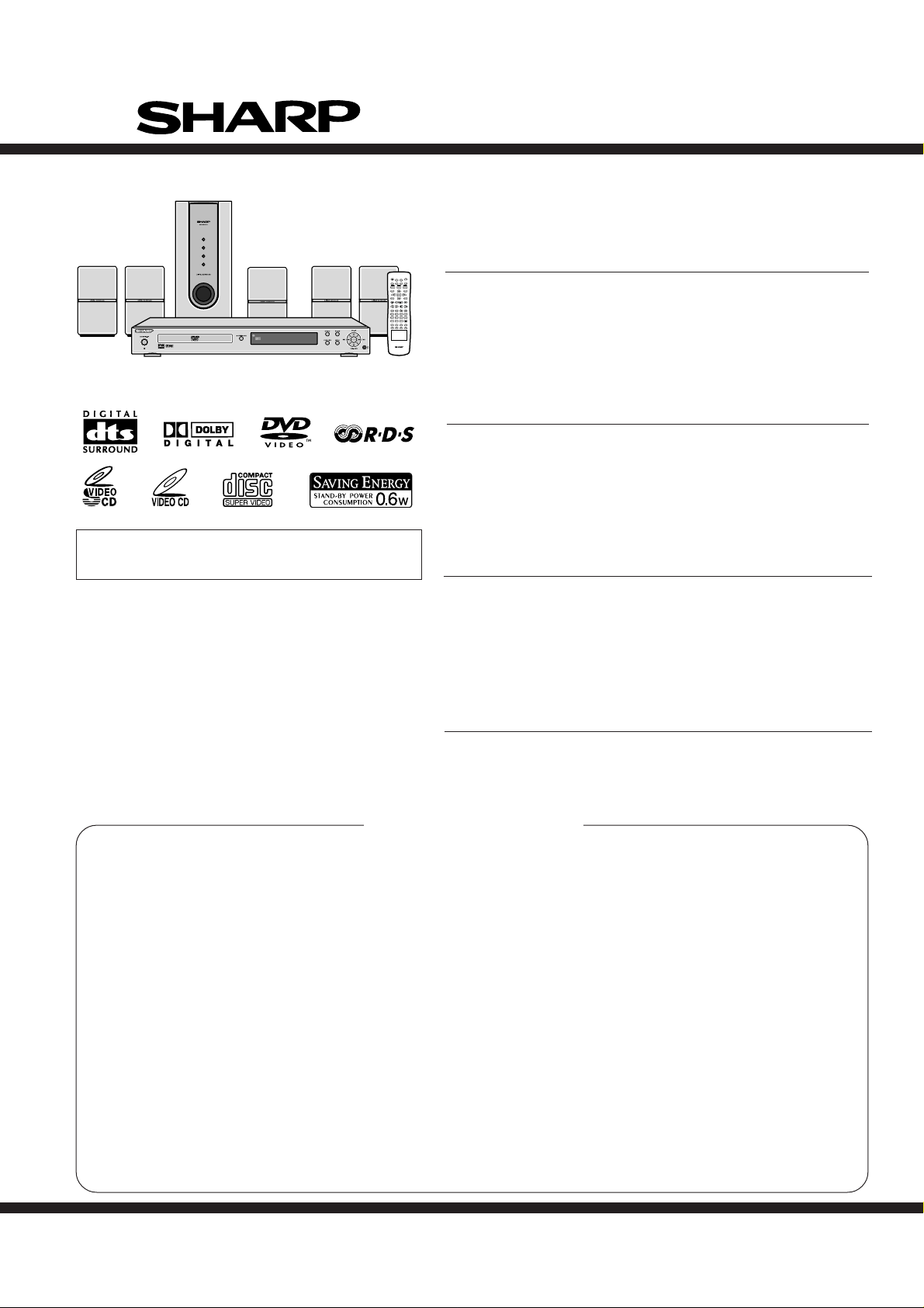
HT-CN400DVH Home Cinema with DVD consisting of HT-CN400DVH
(main unit), CP-CN400HF (front speakers), CP-CN400HC (center
speaker), CP-CN400HR (surround speakers) and CP-CN400HSW.
HOME CINEMA WITH DVD
MODEL HT-CN400DVE
HT-CN400DVE Home Cinema with DVD consisting of HT-CN400DVE
(main unit), CP-CN400EF (front speakers), CP-CN400EC (center
speaker), CP-CN400ER (surround speakers) and CP-CN400ESW.
HOME CINEMA WITH DVD
• In the interests of user-safety the set should be restored to
its original condition and only parts identical to those specified
be used.
MODEL HT-CN500DVH
HT-CN500DVH Home Cinema with DVD consisting of HT-CN500DVH
(main unit), CP-CN500HF (front speakers), CP-CN500HC (center
speaker), CP-CN500HR (surround speakers) and CP-CN500HSW.
HOME CINEMA WITH DVD
MODEL HT-CN500DVE
HT-CN500DVE Home Cinema with DVD consisting of HT-CN500DVE
(main unit), CP-CN500EF (front speakers), CP-CN500EC (center
speaker), CP-CN500ER (surround speakers) and CP-CN500ESW.
CONTENTS
IMPORTANT SERVICE NOTES (FOR HT-CN400DVE/HT-CN500DVE ONLY)............................................................... 2
SAFETY PRECAUTION FOR SERVICE MANUAL ........................................................................................................... 2
SPECIFICATIONS ............................................................................................................................................................. 3
NAMES OF PARTS ........................................................................................................................................................... 5
DISASSEMBLY.................................................................................................................................................................. 7
ADJUSTMENT ................................................................................................................................................................... 9
SW EXTRA FUNCTION..................................................................................................................................................... 9
SOFTWARE UPGRADING & SPECIAL KEY CONTROL ............................................................................................... 10
NOTES ON SCHEMATIC DIAGRAM .............................................................................................................................. 11
TYPES OF TRANSISTOR AND LED............................................................................................................................... 11
BLOCK DIAGRAM ........................................................................................................................................................... 12
SCHEMATIC DIAGRAM .................................................................................................................................................. 14
WIRING SIDE OF P.W.BOARD....................................................................................................................................... 26
VOLTAGE ........................................................................................................................................................................ 32
WAVEFORMS OF DVD CIRCUIT ................................................................................................................................... 36
TROUBLESHOOTING ..................................................................................................................................................... 38
FUNCTION TABLE OF IC................................................................................................................................................ 39
FL DISPLAY..................................................................................................................................................................... 55
REPLACEMENT PARTS LIST/EXPLODED VIEW
PACKING METHOD (FOR U.K. ONLY)
Page
SHARP CORPORATION
This document has been published to be used
for after sales service only.
The contents are subject to change without notice.
Page 2
HT-CN400DVH/HT-CN400DVE/HT-CN500DVH/HT-CN500DVE
PROBE
AC
OUT
UNIT
SHORT-CIRCUIT
AC POWER
SUPPLY CORD
CONNECT THE PROBE
TO GND OF CHASSIS
SCREW
WITHSTANDING
VOLTAGE TESTER
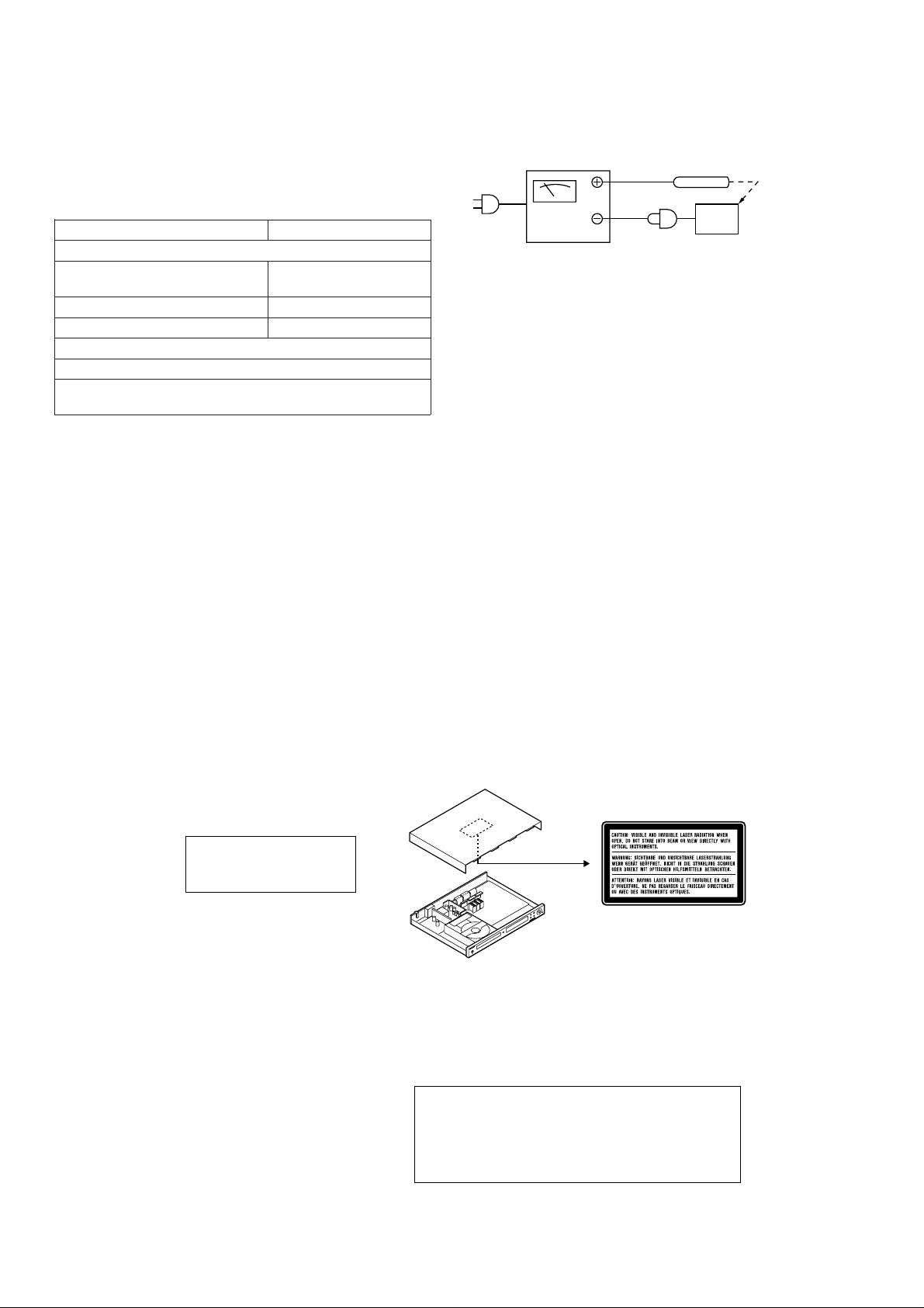
IMPORTANT SERVICE NOTES (FOR HT-CN400DVE/HT-CN500DVE ONLY)
Before returning the unit to the customer after completion of a
repair or adjustment it is necessary for the following withstand
voltage test to be applied to ensure the unit is safe for the
customer to use.
Setting of Withstanding Voltage Tester and set.
Set name set value
Withstanding Voltage Tester
Test voltage 4,240 VPEAK
3,000 VRMS
Set time 6 secs
Set current (Cutoff current) 4 mA
Unit
Judgment
OK: The “GOOD” lamp lights.
NG: The “NG” lamp lights and the buzzer sounds.
SAFETY PRECAUTION FOR SERVICE MANUAL
Precaution to be taken when replacing and servicing the Laser Pickup.
The AEL (Accessible Emission Level) of Laser Power Output for this model is specified to be lower than Class 1 Requirements.
However, the following precautions must be observed during servicing to protect your eyes against exposure to the Laser beam.
(1) When the cabinet has been removed, the power is turned on without a compact disc, and the Pickup is on a position outer than
the lead-in position, the Laser will light for several seconds to detect a disc. Do not look into the Pickup Lens.
(2) The Laser Power Output of the Pickup inside the unit and replacement service parts have already been adjusted prior to shipping.
(3) No adjustment to the Laser Power should be attempted when replacing or servicing the Pickup.
(4) Under no circumstances look directly into the Pickup Lens at any time.
(5) CAUTION - Use of controls or adjustments, or performance of procedures other than those specified herein may result in
hazardous radiation exposure.
Laser Diode Properties
Material: AIGaAs/AIGaInP
Wavelength: 785 nm/650 nm
Emission Duration: continuous
Laser Output: max. 0.6 mW
ADVERSEL-SYNLIG OG USYNLIG LASERSTRÅLING VED ÅBNING. SE IKKE IND I
STRÅLEN-HELLER IKKE MED OPTISKE INSTRUMENTER.
VARO! AVATTAESSA OLET ALTTIINA NÄKYVÄLLE JA NÄKYMÄTTÖMÄLLE
LASERSÄTEILYLLE ÄLÄ TUIJOTA SÄTEESEEN ÄLÄKÄ KATSO SITÄ OPTISEN
LAITTEENLÄPI.
VARNING-SYNLIG OCH OSYNLIG LASERSTRÅLNING NÄR DENNA DEL ÄR
ÖPPNAD. STIRRA EJ IN I STRÅLEN OCH BETRAKTA EJ STRÅLEN GENOM
OPTISKT INSTRUMENT.
VAROITUS! LAITTEEN KÄYTTÄMINEN MUULLA KUIN TÄSSÄ
KÄYTTÖOHJEESSA MAINITULLA TAVALLA SAATTAA ALTISTAA
KÄYTTÄJÄN TURVALLISUUSLUOKAN 1 YLITTÄVÄLLE NÄKYVÄLLE JA
NÄKYMÄTTÖMÄLLE
VARNING - OM APPARATEN ANVÄNDS PÅ ANNAT SÄTT ÄN I DENNA
BRUKSANVISNING SPECIFICERAS. KAN ANVÄNDAREN UTSÄTTAS FÖR
SYNLIG OCH OSYNLIG LASERSTRÅLNING, SOM ÖVERSKRIDER GRÄNSEN
FÖR LASERKLASS 1.
LASERSÄTEILYLLE.
– 2 –
Page 3
FOR A COMPLETE DESCRIPTION OF THE OPERATION OF THIS UNIT, PLEASE REFER
TO THE OPERATION MANUAL.
HT-CN400DVH/HT-CN500DVH
General
Power source
Power consumption
Dimensions
Weight
Audio input terminals
Audio output terminals
Video output terminals
Amplifier (HT-CN400DVH)
Output power
Amplifier (HT-CN500DVH)
Output power
DVD player
Signal system
Supported disc types
Video signal
Audio signal Frequency character-
AC 230 V, 50 Hz
HT-CN400DVH:
Power on: 88 W
Power stand-by: 0.6 W
HT-CN500DVH:
Power on: 105 W
Power stand-by: 0.6 W
Width: 430 mm (16-7/8")
Height: 53 mm (2-1/8")
Depth: 337 mm (13-1/4")
4.2 kg (9.3 lbs.)
Analogue input (IN 1): RCA type 1 pair (L/R)
Analogue input (IN 2): RCA type 1 pair (L/R)
Analogue output (OUT): RCA type 1 pair (L/R)
Headphones: 16 - 50 ohms (recommended: 32 ohms)
SCART output: SCART terminal 1
S-video output: S-terminal 1
Video output: RCA type 1
Front speakers:
RMS: 60 W (30 W + 30 W) (10 % T.H.D., 1 kHz)
Centre speaker:
RMS: 30 W (10 % T.H.D., 1 kHz)
Surround speakers:
RMS: 60 W (30 W + 30 W) (10 % T.H.D., 1 kHz)
Subwoofer:
RMS: 50 W (10 % T.H.D., 100 Hz)
Front speakers:
RMS: 100 W (50 W + 50 W) (10 % T.H.D., 1 kHz)
Centre speaker:
RMS: 50 W (10 % T.H.D., 1 kHz)
Surround speakers:
RMS: 100 W (50 W + 50 W) (10 % T.H.D., 1 kHz)
Subwoofer:
RMS: 50 W (10 % T.H.D., 100 Hz)
PAL/NTSC colour
DVD (Region number 2, ALL), SVCD, VCD, audio CD,
CD-R, CD-RW, MP3
Horizontal resolution: 500 lines
S/N ratio: 70 dB
istics
S/N ratio
Dynamic range
Total harmonic distortion ratio
HT-CN400DVH/HT-CN400DVE/HT-CN500DVH/HT-CN500DVE
SPECIFICATIONS
Tuner
FM: 87.5 -108 MHz
AM: 522 - 1,620 kHz
Full range speaker system (magnetic shield)
8 cm (3-1/8") speaker
HT-CN400DVH: 45 W
HT-CN500DVH: 60 W
HT-CN400DVH: 8 ohms
HT-CN500DVH: 6 ohms
Width: 94 mm (3-3/4")
Height: 169 mm (6-5/8")
Depth: 97 mm (3-7/8")
0.6 kg (1.3 lbs.)/each
Full range speaker system
8 cm (3-1/8") speaker
HT-CN400DVH: 45 W
HT-CN500DVH: 60 W
HT-CN400DVH: 8 ohms
HT-CN500DVH: 6 ohms
Width: 94 mm (3-3/4")
Height: 169 mm (6-5/8")
Depth: 97 mm (3-7/8")
0.6 kg (1.3 lbs.)/each
Sub-woofer system
15 cm (6-1/2") subwoofer
75 W
6 ohms
Width: 135 mm (5-5/16")
Height: 338 mm (13-5/16")
Depth: 375 mm (14-3/4")
5.3 kg (11.7 lbs.)
Linear PCM DVD:
20 Hz to 20 kHz (sampling rate:
48 kHz)
20 Hz to 20 kHz (sampling rate:
96 kHz)
CD: 20 Hz to 20 kHz
CD: 94 dB (1 kHz)
Linear PCM DVD: 95 dB
CD: 94 dB
0.01 % maximum
Frequency range
CP-CN400HF/CP-CN500HF/CP-CN400HC/CP-CN500HC
Type
Maximum input power
Impedance
Dimensions
Weight
CP-CN400HR/CP-CN500HR
Type
Maximum input power
Impedance
Dimensions
Weight
CP-CN400HSW/CP-CN500HSW
Type
Maximum input power
Impedance
Dimensions
Weight
Specifications for this model are subject to change without
prior notice.
– 3 –
Page 4
HT-CN400DVH/HT-CN400DVE/HT-CN500DVH/HT-CN500DVE
HT-CN400DVE/HT-CN500DVE
General
Power source
Power consumption
Dimensions
Weight
Audio input terminals
Audio output terminals
Video output terminals
Amplifier (HT-CN400DVE)
Output power
Amplifier (HT-CN500DVE)
Output power
DVD player
Signal system
Supported disc types
Video signal
Audio signal Frequency character-
AC 230 V, 50 Hz
HT-CN400DVE:
Power on: 88 W
Power stand-by: 0.6 W
HT-CN500DVE:
Power on: 105 W
Power stand-by: 0.6 W
Width: 430 mm (16-7/8")
Height: 53 mm (2-1/8")
Depth: 337 mm (13-1/4")
4.2 kg (9.3 lbs.)
Analogue input (IN 1): RCA type 1 pair (L/R)
Analogue input (IN 2): RCA type 1 pair (L/R)
Analogue output (OUT): RCA type 1 pair (L/R)
Headphones: 16 - 50 ohms (recommended: 32 ohms)
SCART output: SCART terminal 1
S-video output: S-terminal 1
Video output: RCA type 1
Front speakers:
RMS: 60 W (30 W + 30 W) (10 % T.H.D., 1 kHz)
Centre speaker:
RMS: 30 W (10 % T.H.D., 1 kHz)
Surround speakers:
RMS: 60 W (30 W + 30 W) (10 % T.H.D., 1 kHz)
Subwoofer:
RMS: 50 W (10 % T.H.D., 100 Hz)
Front speakers:
RMS: 100 W (50 W + 50 W) (10 % T.H.D., 1 kHz)
Centre speaker:
RMS: 50 W (10 % T.H.D., 1 kHz)
Surround speakers:
RMS: 100 W (50 W + 50 W) (10 % T.H.D., 1 kHz)
Subwoofer:
RMS: 50 W (10 % T.H.D., 100 Hz)
PAL/NTSC colour
DVD (Region number 2, ALL), SVCD, VCD, audio CD,
CD-R, CD-RW, MP3
Horizontal resolution: 500 lines
S/N ratio: 70 dB
istics
S/N ratio
Dynamic range
Total harmonic distortion ratio
Linear PCM DVD:
20 Hz to 20 kHz (sampling rate:
48 kHz)
20 Hz to 20 kHz (sampling rate:
96 kHz)
CD: 20 Hz to 20 kHz
CD: 94 dB (1 kHz)
Linear PCM DVD: 95 dB
CD: 94 dB
0.01 % maximum
Tuner
Frequency range
CP-CN400EF/CP-CN500EF/CP-CN400EC/CP-CN500EC
Type
Maximum input power
Impedance
Dimensions
Weight
CP-CN400ER/CP-CN500ER
Type
Maximum input power
Impedance
Dimensions
Weight
CP-CN400ESW/CP-CN500ESW
Type
Maximum input power
Impedance
Dimensions
Weight
Specifications for this model are subject to change without
prior notice.
FM: 87.5 -108 MHz
AM: 522 - 1,620 kHz
Full range speaker system (magnetic shield)
8 cm (3-1/8") Speaker
HT-CN400DVE: 45 W
HT-CN500DVE: 60 W
HT-CN400DVE: 8 ohms
HT-CN500DVE: 6 ohms
Width: 94 mm (3-3/4")
Height: 169 mm (6-5/8")
Depth: 97 mm (3-7/8")
0.6 kg (1.3 lbs.)/each
Full range speaker system
8 cm (3-1/8") Speaker
HT-CN400DVE: 45 W
HT-CN500DVE: 60 W
HT-CN400DVE: 8 ohms
HT-CN500DVE: 6 ohms
Width: 94 mm (3-3/4")
Height: 169 mm (6-5/8")
Depth: 97 mm (3-7/8")
0.6 kg (1.3 lbs.)/each
Sub-woofer system
15 cm (6-1/2") Subwoofer
75 W
6 ohms
Width: 135 mm (5-5/16")
Height: 338 mm (13-5/16")
Depth: 375 mm (14-3/4")
5.3 kg (11.7 lbs.)
– 4 –
Page 5
HT-CN400DVH/HT-CN400DVE/HT-CN500DVH/HT-CN500DVE
p
p
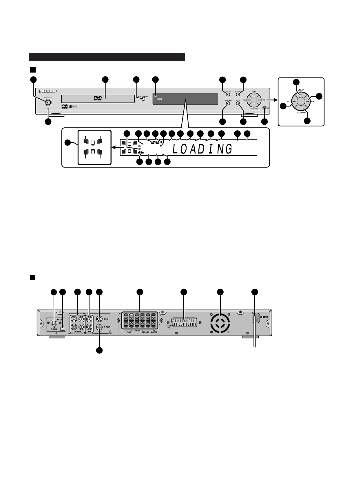
NAMES OF P ARTS
HT-CN400DVH/HT-CN400DVE/HT-CN500DVH/HT-CN500DVE
Main unit (front panel)
1
2
3
4
5
6
12
13
11
7
(1)
(3)(2)
RL
14
C
S
RSLS
(4) (6)(5)
1. On/Stand-by Button
2. Disc Tr ay
3. Disc Tray Open/Close Button
4. Remote Sensor
5. Play or Pause Button
6. Stop Button
7. Power Stand-by Indicator
8. Function Button
9. Speaker Level Mode Button
10. Headphone Socket
11. Chapter (track) Skip Down or Tuning Down Button
12. Volume Up and Down or Speaker Level Adjust Buttons
13. Chapter (track) Skip Up or Tuning Up Button
14. Speaker Indicators
(1) Left Front Speaker Indicator (4) Left Surround Speaker Indicator
(2) Centre Speaker Indicator (5) Subwoofer Indicator
(3) Right Front Speaker Indicator (6) Right Surround Speaker Indicator
15 16
RL
C
S
RSLS
28 29 30 31
DIGITAL
Pro Logic
CD MP3STEREO V
Main unit (rear panel)
8 9
222117 18 19 20
REPEAT1SLEEPPROGCHPPRESETTRKTITLE
10
2726252423
A-B
KHz
MHz
15. Dolby Pro Logic Indicator
16. Dolby Digital Signal Indicator
17. DVD Indicator
18. Pause Indicator
19. Play Indicator
20. Title Indicator
21. Track Indicator
22. Tuner Preset Indicator
23. Chapter Indicator
24. Programme Indicator
25. Sleep Indicator
26. Repeat Indicator
27. A - B Repeat Indicator
28. DTS Signal Indicator
29. Stereo (2-ch) or FM Stereo Receiving Indicator
30. SVCD/VCD/CD Indicator
31. MP3 or JPEG Indicator
12
2 3104 5 7 96 8
1
1. FM 75 Ohms Aerial Socket
2. AM Loop Aerial Socket
3. Audio Input Sockets 1/2
4. Audio Output Sockets
5. Video Out
ut Socket
6. Speaker Terminals
7. SCART Output Socket
8. Cooling Fan
9. AC Power Lead
10. S-video Out
ut Socket
– 5 –
Page 6
HT-CN400DVH/HT-CN400DVE/HT-CN500DVH/HT-CN500DVE
HT-CN400DVH/HT-CN400DVE/HT-CN500DVH/HT-CN500DVE
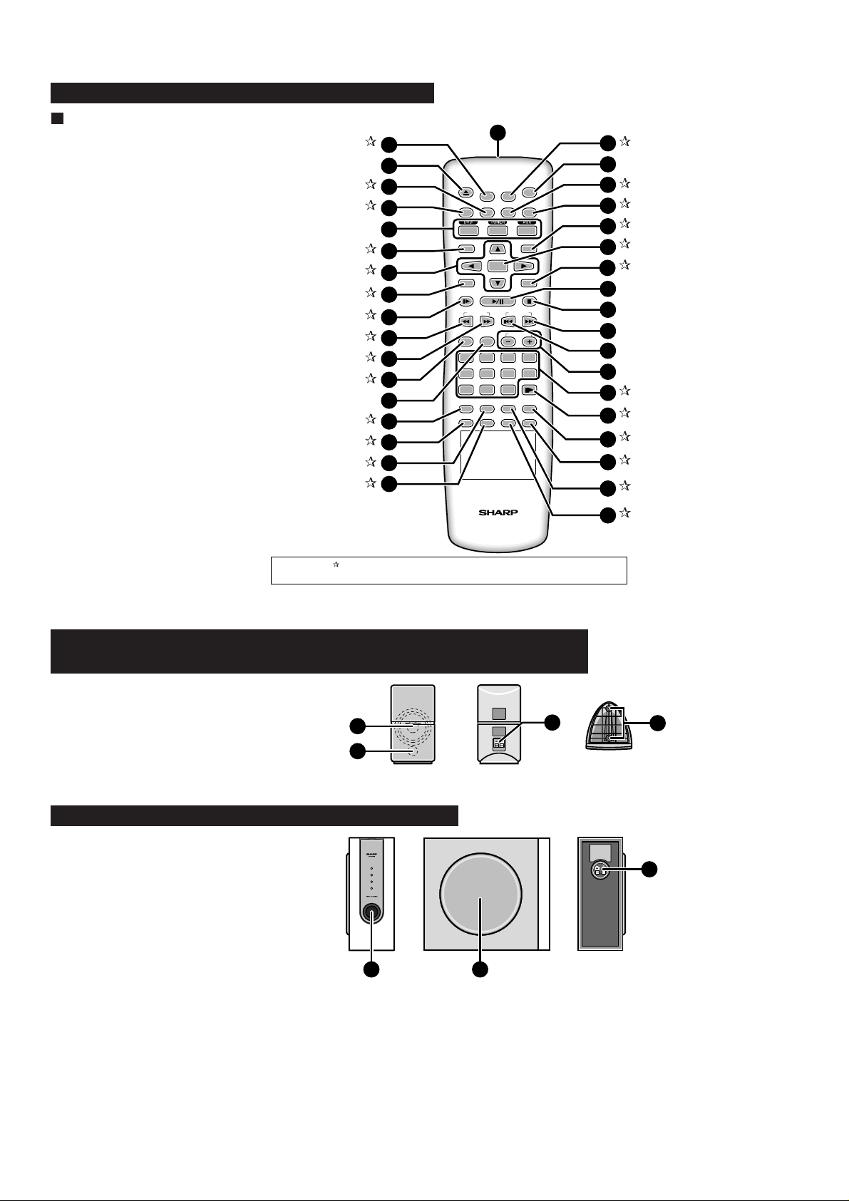
Remote control
1. Remote Control Transmitter
2. Set Up Menu Button
3. Disc Tray Open/Close Button
4. Subtitle Select Button
5. Title Select Button
6. DVD/Tuner/Auxiliary Input Select Buttons
7. Menu/Playback Control On/Off Button
8. Cursor Buttons
9. Programme Button
10. Slow-motion or Preset Memory Button
11. Fast Reverse or Preset Down Button
12. Fast Forward or Preset Up Button
13. Surround/Stereo (2-ch) Listening Mode Button
14. Speaker Level Mode Button
15. Direct Button
16. Angle Select Button
17. Return Button
18. Zoom Button
19. Mute Button
20. On/Stand-by Button
21. Language Select Button
22. Display Button
23. FM Stereo/Mono Select Button
24. Enter Button
25. Sleep Button
26. Play or Pause Button
27. Stop Button
28. Chapter (track) Skip Up or Tuning Up Button
29. Chapter (track) Skip Down or Tuning Down Button
30. Volume Up and Down or Speaker Level Adjust Buttons
31. Direct Number Buttons
32. Frame Advance Button
33. A - B Repeat Button
34. NTSC/PAL Select Button
35. Repeat Play Button
36. Audio Select Button
10
12
13
14
15
16
17
18
11
2
1
3
OPEN/
CLOSE
TITLE
MENU/PBC
SET UP
SUBTITLE
4
5
6
MUTE
LANGUAGE
ON/
STAND-BY
DISPLAY
ST/MO
7
ENTER
8
9
PROG
SLOW/MEMORY
PRESET
LISTENING
9
DIRECT
ANGLE
RETURN
MODE
>
0
REPEAT
ZOOM AUDIO
TUNING
ADJ/VOL
321
10
SLEEP
4
8765
STEP
A-B
NTSC/PAL
19
20
21
22
23
24
25
26
27
28
29
30
31
32
33
34
35
36
Buttons with " " mark in the illustration or highlighted in bold on the list can be operated on the remote control only.
CP-CN400HF/CP-CN400HC/CP-CN400HR/CP-CN400EF/CP-CN400EC/CP-CN400ER/
CP-CN500HF/CP-CN500HC/CP-CN500HR/CP-CN500EF/CP-CN500EC/CP-CN500ER
1. Speaker
2. Bass Reflex Duct
3. Speaker Terminals
4. Mounting Holes for Stand or Bracket
1
2
CP-CN400HSW/CP-CN400ESW/CP-CN500HSW/CP-CN500ESW
1. Bass Reflex Duct
2. Woofer
3. Speaker Terminals
21
3
4
3
– 6 –
Page 7
HT-CN400DVH/HT-CN400DVE/HT-CN500DVH/HT-CN500DVE
(D1)x4
ø3x6mm
(C1)x6
ø3x6mm
Front
Panel
Loading Tray
Mechanism
Main PWB
Power PWB
(B2)x1
(B1)x4
ø3x6mm
(B1)x7
ø3x8mm
Rear Panel
Fan Motor
SCART PWB
Main PWB
Front
Panel
(B2)x2
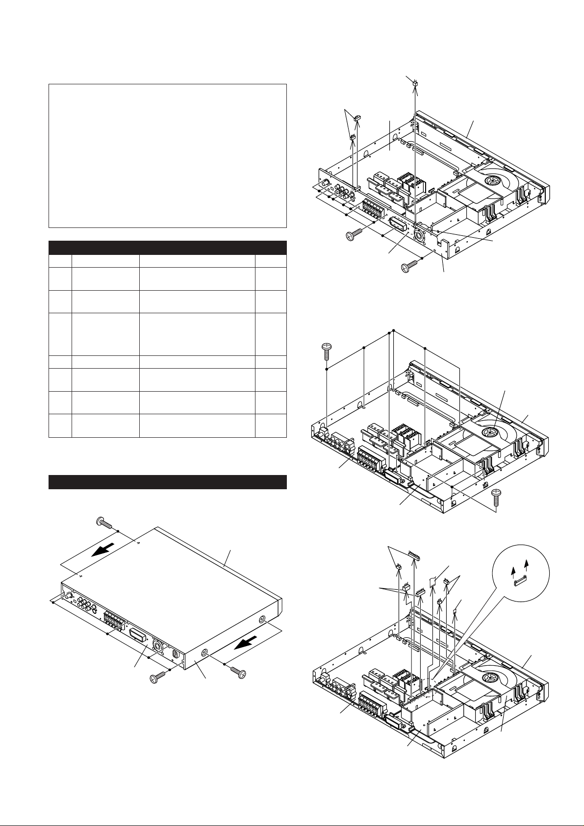
DISASSEMBLY
Caution on Disassembly
Follow the below-mentioned notes when disassembling
the unit and reassembling it, to keep it safe and ensure
excellent performance:
1. Take dvd disc out of the unit.
2. Be sure to remove the power supply plug from the wall
outlet before starting to disassemble the unit.
3. Take off nylon bands or wire holders where they need to
be removed when disassembling the unit. After servicing
the unit, be sure to rearrange the leads where they were
before disassembling.
4. Take sufficient care on static electricity of integrated
circuits and other circuits when servicing.
HT-CN400DVH/HT-CN400DVE/HT-CN500DVH/HT-CN500DVE
STEP REMOVAL PROCEDURE FIGURE
1 Top Cabinet 1. Screw ...................... (A1) x9 7-1
2. Pull to the arrow direction.
2 Rear Panel/Scart 1. Screw .................... (B1) x11 7-2
PWB/Fan Motor 2. Socket ..................... (B2) x3
3 Main PWB 1. Screw ...................... (C1) x6 7-3
- 2. Socket ..................... (C2) x6 7-4
Figure 7-2
3. Flat Cable ............... (C3) x2
4 Power PWB 1. Screw ...................... (D1) x4 7-3
5 Front Panel 1. Screw ...................... (E1) x8 8-1
2. Hook........................ (E2) x2
6 Display/Switch 1. Screw .......................(F1) x9 8-2
PWB
7 Headphones 1. Screw ...................... (G1) x1 8-2
PWB 2. Bracket .................... (G2) x1
HT-CN400DVH/HT-CN400DVE/HT-CN500DVH/HT-CN500DVE
(A1)x2
ø3x6mm
Front
Panel
Pull
(C2)x2
(C2)x2
Figure 7-3
(C3)x1
(C2)x2
(C3)x1
Rear Panel
(A1)x5
ø3x6mm
Figure 7-1
Pull
Top Cabinet
(A1)x2
ø3x6mm
– 7 –
Main PWB
Power PWB
Front
Panel
Loading
Tray Mechanism
Figure 7-4
Page 8
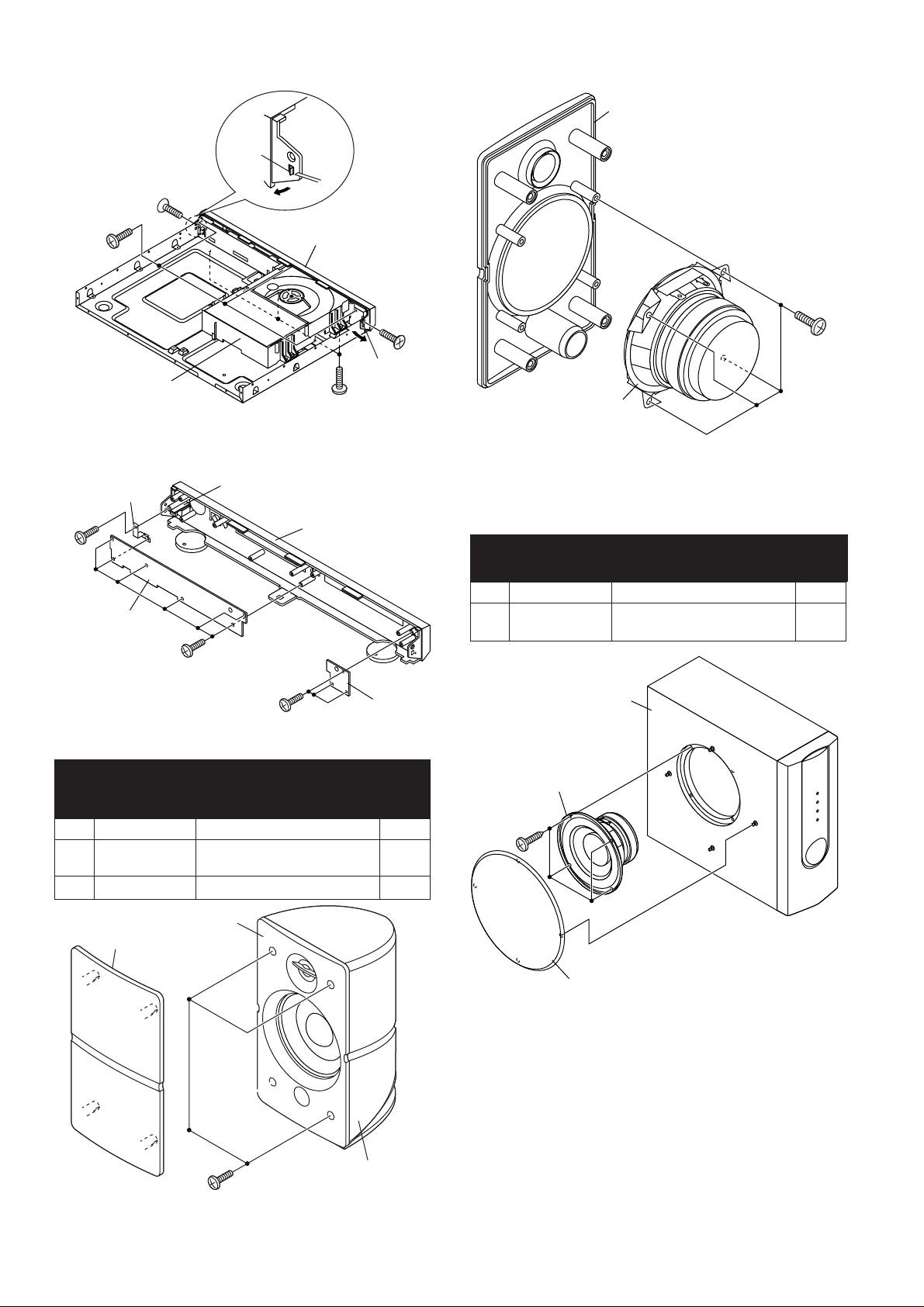
HT-CN400DVH/HT-CN400DVE/HT-CN500DVH/HT-CN500DVE
(E2)x1
(E1)x1
ø3x4mm
Front
(E1)x3
ø3x8mm
Panel
(E1)x1
ø3x4mm
Front Panel
(B1)x4
ø3x8mm
Loading Tray
Mechanism
(E1)x3
ø3x6mm
(E2)x1
Figure 8-1
Headphones PWB
(G1)x1
ø3x8mm
(G2)x1
Display PWB
(F1)x6
ø3x8mm
(F1)x3
ø3x8mm
Front
Panel
Switch PWB
Figure 8-2
CP-CN400HF/CP-CN400HC/CP-CN400HR/CP-CN400EF/
CP-CN400EC/CP-CN400ER/CP-CN500HF/CP-CN500HC/
CP-CN500HR/CP-CN500EF/CP-CN500EC/CP-CN500ER
STEP REMOVAL PROCEDURE FIGURE
1 Front panel 1. Net Frame Ass'y .... (A1) x1 8-3
2. Screw ..................... (A2) x4
2 Speaker 1. Screw ..................... (B1) x4 8-4
Speaker
Figure 8-4
CP-CN400HSW/CP-CN400ESW/
CP-CN500HSW/CP-CN500ESW
STEP REMOVAL PROCEDURE FIGURE
1 Speaker 1. Net Frame Ass'y .... (A1) x1 8-5
2. Screw ..................... (A2) x4
Speaker Box
Speaker
(A2)x4
ø4x14mm
(A1)x1
Front Panel
(A1)x1
Figure 8-5
Speaker Box
(A2)x4
ø3x12mm
Figure 8-3
– 8 –
Page 9
HT-CN400DVH/HT-CN400DVE/HT-CN500DVH/HT-CN500DVE
TUNER SECTION
fL: Low-range frequency
fH: High-range frequency
••
•
AM IF/RF
••
Signal generator: 400 Hz, 30%, AM modulated
Test Stage Frequency Frequency
Display
AM IF 450 kHz 1,620 kHz T351 *1
AM Band — 522 kHz (fL): T306 *2
Coverage 1.4 ± 0.1 V
AM Tracking 990 kHz 990 kHz (fL): T302 *1
*1. Input: Antenna Output: TP302
*2. Input: Antenna Output: TP301
Setting/
Adjusting
Parts
ADJUSTMENT
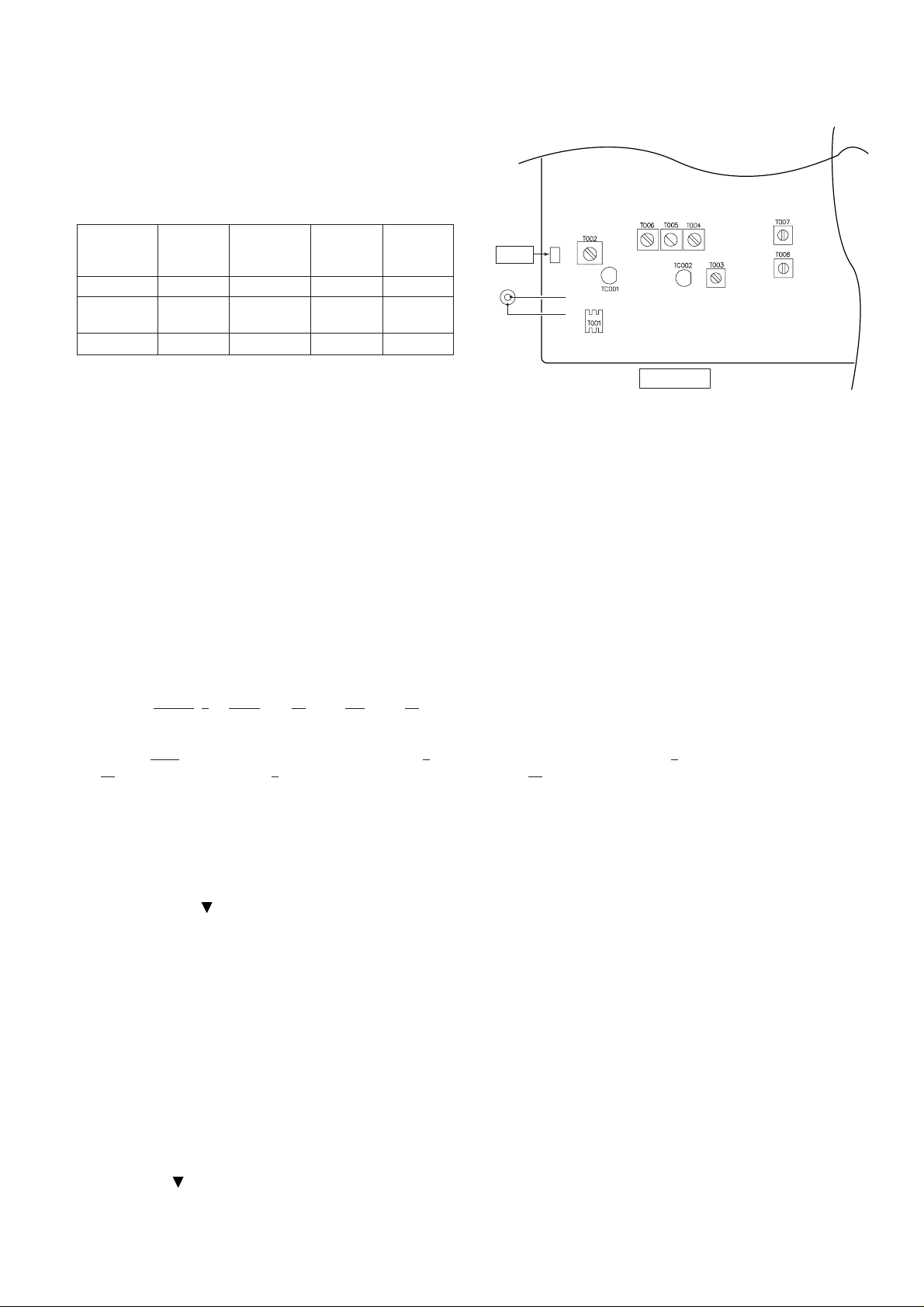
Instrument
Connection
AM LOOP
ANTENNA
FM ANTENNA
JK001
2
1
MAIN PWB
• FM IF
Figure 9 TUNER ADJUSTMENT POINTS
Notes:
1: Description of the "FM IF Adjustment" is not carried on this
Manual. It is because the IF coil in the FM front end section
has been best adjusted in the factory so that its further
adjustment is not needed at the field. When replacing the
FM front end assembly, no adjustment is needed either.
2: The parts in the FM front end section are prepared in a
complete unit, so you can't obtain each part individually.
SW EXTRA FUNCTION
1. How to show Version number.
A. Door Open,
B. Press and hold R/C "Volume up" Button;
C. Press R/C "Zoom" button continue,
D. OSD show version number,
VER
Month and day version TV TYPE Tuner area region code LANGUAGE
The first
xx for tuner area, the fifth x stand for region code. The sixth code xx stand for language.
2. How to adjust TUNER AREA.
A. Door Open
B. Press and hold R/C "Volume up" button;
C. Press R/C "Subtitle" button continue;
D. OSD show "Tuner Area: xx
E. Then use R/C
F. If OK button is pressed in five seconds, OSD will show "Tuner Area Change"; If you didn't press it in five seconds, the system
xxxx x PAL xx x xx
xxxx stand for month and day, the second x stand for version sequence, the third x stand for TV system, the forth
Press Down button to select
Press OK button to confirm"
to select tuner area you want (EUR USA cyclically), then press " OK" to confirm,
will remain original status.
3. How to select OSD Language Sequency,
A. Door close and no disc,
B. Press and hold R/C "Volume up" button;
C. Then Press R/C "Subtitle" button;
D. OSD show last setting "OSD language", (English -> France -> German -> Italian -> Spanish).
E. Then use
button to select language that you want and its sequence.
F. For example: default language is English, you select English and press Enter button, then its sequence is change to
(English -> France -> German -> Italian -> Spanish)
– 9 –
Page 10

HT-CN400DVH/HT-CN400DVE/HT-CN500DVH/HT-CN500DVE
SOFTWARE UPGRADING & SPECIAL KEY CONTROL
1. Software Upgrading
a) Burn the software "bank30.rom" in CD-R/CD-RW (lower burning speed is recommended).
b) Load CD-R/CD-RW in DVD receiver.
c) After finished loading, VFD will show "Read" and OSD will display "Reading".
d) After reading, system will start upgrading software, VFD will show "Update" and OSD will
display "Erase" then "Writing".
* If fail to upgrade, OSD will display "Checksum error". Turn off/on power and try upgrading
again. If still fail, re-burn CD-R/CD-RW.
e) After finished "Writing", VFD and OSD will display "Done" then tray will open automatically.
* If the tray did not open automatically, just proceed to next step (f).
f) Unplug and plug in AC power cord or turn off and on main power supply.
g) Turn on power and confirm the software version.
g). Defaults the reset => Power on the set, press “set up” button at remote control, SETUP menu will display at TV screen,
go to enter PREFERENCES. At Preferences Page, go to Defaults-Reset and enter the Reset.
Caution : DO NOT disturb or cut off power supply during software upgrading, it will cause the data
lost. Hence the flash IC have to be burned software again.
2. Special Key Control
a) Software version i) On Tray open condition.
ii) Press and hold remote controller key "Volume up" for 2 seconds.
iii) Release "Volume up"key then press "Zoom" key.
iv) OSD will display " VER xxxx x yy z ".
Where xxxx xis Version number
yy is Tuner area
z is Region code
b) Tuner Area i) On Tray open condition.
ii) Press and hold remote controller key "Volume up" for 2 seconds.
iii) Release "Volume up"key then press "Subtitle" key.
iv) OSD will display "Tuner area".
v) Follow OSD instruction to change the tuner area
vi) After tuner area was changed, the preset station will be initialized at default station.
d) OSD Language i) On No disc condition.
ii) Press and hold remote controller key "Volume up" for 2 seconds.
iii) Release "Volume up"key then press "Subtitle" key.
iv) OSD will display "OSD Language".
v) Follow OSD instruction to change the OSD language.
– 10 –
Page 11
HT-CN400DVH/HT-CN400DVE/HT-CN500DVH/HT-CN500DVE
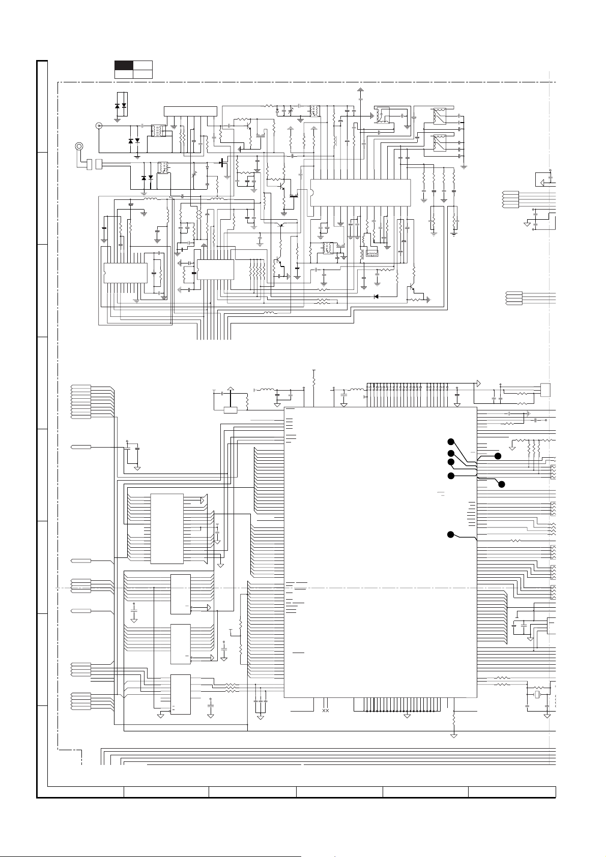
NOTES ON SCHEMATIC DIAGRAM
• Resistor:
To differentiate the units of resistors, such symbol as K and
M are used: the symbol K means 1000 ohm and the symbol
M means 1000 kohm and the resistor without any symbol is
ohm-type resistor. Besides, the one with “Fusible” is a fuse
type.
• Capacitor:
To indicate the unit of capacitor, a symbol P is used: this
symbol P means pico-farad and the unit of the capacitor
without such a symbol is microfarad. As to electrolytic
capacitor, the expression “capacitance/withstand voltage”
is used.
(CH), (TH), (RH), (UJ): Temperature compensation
(ML): Mylar type
(P.P.): Polypropylene type
• Schematic diagram and Wiring Side of P.W.Board for this
model are subject to change for improvement without prior
notice.
• The indicated voltage in each section is the one measured
by Digital Multimeter between such a section and the chassis with no signal given.
1. In the tuner section,
indicates AM
indicates FM stereo
2. In the power section, a tape is being played back.
• Parts marked with “ 1 ” ( ) are important for
maintaining the safety of the set. Be sure to replace these
parts with specified ones for maintaining the safety and
performance of the set.
REF. NO
TA301 ON/STAND-BY ON—OFF
TA302 STOP ON—OFF
TA303 FAST FORWARD ON—OFF
TA304 FAST REVERSE ON—OFF
TA305 VOLUME DOWN ON—OFF
TA306 MODE ON—OFF
TA307 FUNCTION ON—OFF
TA308 VOLUME UP ON—OFF
TA309 PLAY ON—OFF
TA310 OPEN/CLOSE ON—OFF
DESCRIPTION
POSITION
FRONT
VIEW
E B C
(S) (D) (G)
PN222 A
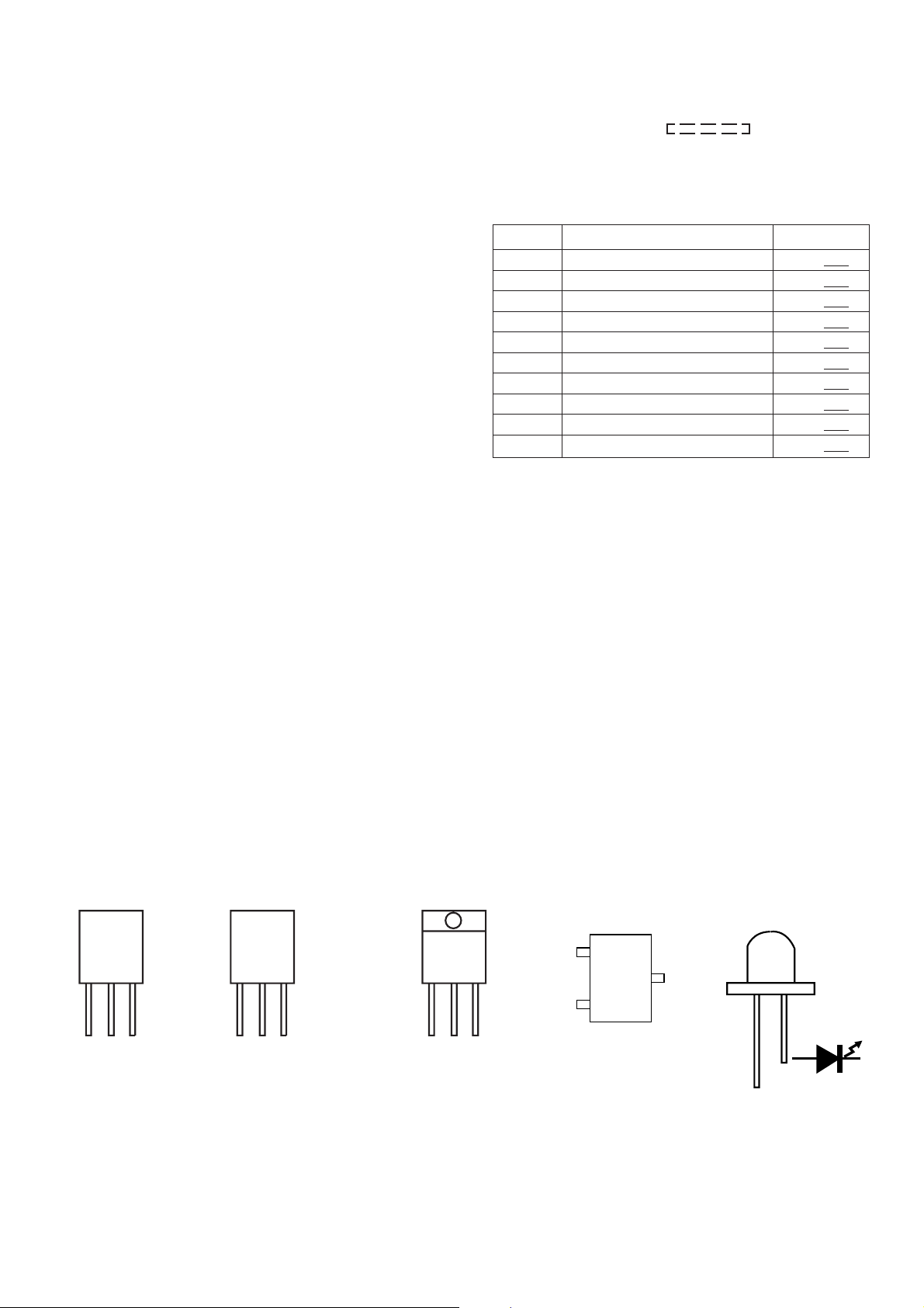
TYPES OF TRANSISTOR AND LED
FRONT
VIEW
E C B
(S) (G) (D)
(1) (2) (3)
2SC2001 L 2TIP122 DDTC114 ECA
FRONT
VIEW
B C E
– 11 –
B
(3)
E
(1)
CM5783 GR
2SC1009 A
2SC1623
CM5051
2SA812
TOP
VIEW
(2)
C
KER00022SK192 A
VIEW
FRONT
Page 12
HT-CN400DVH/HT-CN400DVE/HT-CN500DVH/HT-CN500DVE
E
D
u
T
M
D
D
M
W
P
DVD MECHANISM UNIT
MAIN BOARD
LOADER
IC801
DVD MOTOR
Drive IC
LA6560
IC802
DVD Servo RF IC
LA9703W
SDRAM
256K
DVD Servo Control
74LS157
Digital Audio Select
IC803
LC78663W
I/O PORT
74HC32
74HC14
EXPAND
I/O PORT
74LS374*3
DATA
FLASH
8M
2CH AUDIO A/D
AUX1
AUX2
FM
AM
TUNER
LA1837
PLL: LA72131
RDS: LC72720
TUNER BOARD
IC110
2CH AUDIO A/D
AUDIO
INPUT
SELECT
CD4052
Figure 12 BLOCK DIAGRAM (1/2)
– 12 –
AUDIO BUFFER
JRC4558
WM8772
6CH AUDIO D/A
FLFRCSLSR
FILTER
JRC4558*3
C
SL
FR
SR
SUB
SUB
FL
Page 13
HT-CN400DVH/HT-CN400DVE/HT-CN500DVH/HT-CN500DVE
FLASH
8M
4*16M 24C02
IC106
ESS6028
MPEG II Decoder
DTS Decoder
DOLBY DIGITAL Decoder
DOLBY PROG LOGIC Decoder
WMA Decoder
MP3 Decoder
TV ENCODE
Progressive Scan
u-com
KEY ARRAY VFD
EEPROMSDRAM
PANNEL BOARD
PIC16C54C
PT6311
POWER BOARD
POWER BOARD
PANNEL BOARD
S-VIDEO
CVBS
VIDEO FILTER
DIGITAL OUT
Y
Pb
Pr
SCART
OPTICAL
COAXIAL
L
R
FL
FR
C
SL
SR
SUB
MIC A/D
WM8739
Digital Audio Processo
Bass and Treble Control
6CH Volume Control
Bass management
DX-8000
PHONE VOLUME
PT2259
DOWNMIXING
JRC4558
MICAMP
JRC4558
FL
POWER
AMPLIFIER
DDX-2100*2
DDX-2100*3
L
R
LT=L-0.707SL-0.707SR+0.707C
RT=R+0.707SL+0.707SR+0.707C
FR
C
SL
SR
SUB
PHONEAMP.
TP5228
FILTER
Microphone
INPUT
FL
FR
C
SL
SR
SUB
SPEAKER OUT
PHONE
OUTPUT
LT
RT
LINE OUT
FR
FL
C
SL
SR
SUB
Figure 13 BLOCK DIAGRAM (2/2)
– 13 –
Page 14
HT-CN400DVH/HT-CN400DVE/HT-CN500DVH/HT-CN500DVE
3
0
0
0
0
0
C
4
P
0
5
SITUATION :
R034
L002 39uH
AM RF
AMIF
CF003
450KHz
C110
104
51
AVCC(PLL)
C018
33UF
C020
33UF
C021 22UF
AFC
AM AGC
GND
TU LED
C024
T004 TSHV1492-003
220PF
C019
223
C023 10UF
C022 M153
R033 1K
C075 331
232221
24252627282930
2019181716
MPXL
MPXR
NPXIN
AM DEC
IC001
FM DEC
ST LED
VCC ENDEC
FM SD
AM CF
9
8
10
223
C028
273R020
R018 100OHM
51 OHM
C031 47U F
C030
C029 473
C032
R019
2.7K
10uH
L003
T007
C036
223C074
223
D005
1N4148
C111-C134(104)
FB104
VC33
5968759299
VC33
VC33
VC33
VC33
VC33
IC106
ES6028
MICROCOMPUTER
VSS8VSS17VSS
VSS
VSS
AVSS(PLL)52VSS60VSS67VSS76VSS84VSS
26
34
43
TSHV1492-004
T005
C039
C025
10UF
30PF
C040
10UF
TSHV1492-004
C049 152
C048 152
R027
R028
5.6K
RIN
LIN
LOUT
AM SD
MUTE IF
AM/FM
12
131411
3K
4.7K
R021
1UF
R022
0.47UF
C038
1UF
C037
R024
R023
3.9K
4.7K
104
130
148
157
VC33
VC33
VC33
VC33
VC33
VC33
VSS98VSS
91
103
120
6.8K
ROUT
M153
4.7UF
C050
C051
VCO
R031
15
2.2K
C054
472
1UF
C041
IC001
LA1837
R025
4.7K
Q006
C945
R026
47K
9
3518318121
44
159
164
183
193
201
VC27
VC27
VC27
VC33
VC33
VC33
VC33
VC33
VC33
VSS
VSS
VSS
VSS
VSS
VSS
VSS
VSS
VSS
VSS
129
138
147
156
163
171
177
184
192
222
C044
C046
223
C043
C045
T006
R029
R030
5.6K
6.8K
M153
4.7UF
C052
C053
2.2K
C055
472
R032
VCC27
C135
10UF
13927172
YUV0/CAMYUV2
YUV1/VREF
VC27
VC27
VC27
VC27
YUV2/CDAC
YUV3/COMP
YUV4/RSET
AVSS(VDAC)
YUV5/YDAC
YUV6/VDAC
YUV7CAMYUV3
1
TDMTSC
2
3
TWS/SEL_PLL2
TSD0/SEL_PLL0
TSD1/SEL_PLL1
4
PCLK2XSCN/CAMYUV4
PCLKQSCN/CAMYUV5/AUX3[2]
VSSCN/CAMYUV6/EAUX3[1]
HSSCN/CAMYUV7/EAUX3[0]
DSCK/DOE
DBANK0/DRAS1
DBANK1/DRAS2
11
SPDIF/SEL_PLL3
NC/APLL
VSS
VSS
41
48
200
208
R116
4.7K
C042
472
222
472
C047
223
SD2
SD1
SD0
LRCK
BICK
RST
AUX0
AUX1
AMCLK
VCC
R145 120 OHM
C1008
C1007
104
104
VREF
C136 104
R104
5DAC
OK_DA
10
5
60 OHM at 100MHz
DMA0
DMA1
DMA2
DMA3
DMA4
DMA5
DMA6
DMA7
DMA8
DMA9
DMA10
DMA11
DB0
DB1
DB2
DB3
DB4
DB5
DB6
DB7
DB8
DB9
DB10
DB11
DB12
DB13
DB14
DB15
AUX0
AUX1
VFD-DA
RDS-DI
YU-D
SD
HWAITB
R113 33 OHM
R114 33 OHM
R146 150 OHM
270 OHM
R109
0 OHM
MCLK
TBCK
TWS
TSD0
TSD1
TSD2
R112
B5V
C138
10UF 104
DRAS0
DMA10
DMA11
SPDIFOSPDIFIN
106
107
108
109
110
112
113
114
115
47
RBCK
46
RWS
45
RSD
31
39
MCLK
40
TBCK
32
33
36
37
TSD2
TSD3
38
116
117
118
119
69
DCAS
70
71
DWE
72
73
74
97
DCS1
100
DCS0
101
DQM
102
DSCK
53
DMA0
54
DMA1
55
DMA2
56
DMA3
57
DMA4
58
DMA5
61
DMA6
62
DMA7
63
DMA8
64
DMA9
65
66
77
DB0
78
DB1
79
DB2
80
DB3
81
DB4
82
DB5
85
DB6
86
DB7
87
DB8
88
DB9
89
DB10
90
DB11
93
DB12
94
DB13
95
DB14
96
DB15
160
AUX0
161
AUX1
162
AUX2
165
AUX3
166
AUX4
167
AUX5
168
AUX6
169
AUX7
49
XIN
50
XOUT
105
CLK
+2.5V
C
1
SD2
SD1
SD0
LRCK
BICK
+3.3V
C510
104
C511
104
+2.5V
RST
AUX0
AUX1
AMCLK
3
2
1
IC115
RT9164-CG
104
C137
VCC3
R105
OPEN
R107 4.7K
R106 4.7K
R108 4.7K
R110
R111
RA1
1
2
3
4
ENCODE1
ENCODE2
RA1
4
3
2
1
R160
R161
R162
R163
RA1
4
3
2
1
RA1
4
3
2
1
RA1
4
3
2
1
8
VCC
7
WC
6
SCL
5
SDA
C139
CLK
R115 56K
27MHz
22PF
C140
I
TA2
EE
XL101
C141
22PF
1N4148
1N4148
A
AM
LOOP
ANTENNA
B
IC003
LC72720NM
C
D
TCLOSE-SW
TOPEN-SW
TRAY-REV
TRAY-FWD
DMUTE
OSCIN
DCLK
HIRQB
LWRHL
LOE#
LSW
1
2
JK001
CN001
CON2
TCLOSE-SW
TOPEN-SW
LSW
TRAY-REV
TRAY-FWD
DMUTE
OSCIN
DCLK
HIRQB
LWRHL
ESD1
1
2
C072 10UF
1234567891011
VREF
VSSA
VDDA
NPXIN
SYR
24
LOE#
ESD2
C001
33PF
D001 1N4148
D002 1N4148
1N4148
D003
D004 1N4148
R059 10OHM
C071
47UF
R055
4.7K
C069
47UF
R056 4.7K
C070 561
12
T1T2T3T4T5
CIN
FLO
XOUTXIN
VDD14VSS15T616T717SYNC
13
18
19D020CL21DI22CE23
VCC
C102
10UF
C101
104
E
A16
1
A15
2
A14
3
4
A13
5
A12
6
A11
7
A9
A8
8
WRLL#
IC101
SST39VF080
MULTI-PURPOSE FLASH
HD[0..7]
HD[0..7]
F
G
H
DCI_ERR
HCLK#
HDACK#
DCI_REQ
DCI_FDS
EAUX40
TDMDR
TDMCLK
TDMFS
HIRQB
DCI_ERR
HCLK#
HDACK#
DCI_REQ
DCI_FDS
EAUX40
TDMDR
TDMCLK
TDMFS
LCS1#
LCS1#
HIRQB
FGO
FGO
RESB
RESB
GU
GU
TCLOSE-SW
TOPEN-SW
9
10
11
12
A18
13
A7
14
A6
15
A5
16
17
A4
18
A3
19
A2
20
A1
72CE
72CLK
72DA
DVD
S-B
S-A
S-BLNK
S-SWTCH
VCC
C104
104
VFDCE
VFDCLK
LMUTE
MUTE
2259DA
2259CL
WM8739CE
DOUT
BICK
LRCK
QUAD 2:1 MULTIPLEXER
TUNER PACK
ANT
ANT
1NC2
T001
CON3
T002
AHV0491-101
3
2
451
R060
10OHM
C068
22PF
XL002 4.332MHz
R054 10K
C067
22PF
A16
A15
A14
A13
A12
A11
A9
A8
WE#
IC101
NC
NC
NC
A18
A7
A6
A5
A4
A3
A2
A1 A0
2
5
6
9
12
15
16
19
IC102
IC102
74F374D
IC103
2
5
6
9
12
15
16
19
IC103
IC103
74HC374
2
1A
3
1B
5
2A
6
2B
11
3A
10
3B
14
4A
13
4B
1
A/B
15
G
IC104
SN74F157A
TRAY-REV
TRAY-FWD
EF001
NC
AGC
GNDVTB+
AG
GNDVTB+3IF/O
45678
R002 100K
R001 6.8K
C007 104
R052
1K
C064
47UF
223
C063
C065
104
C066
102
C058
15PF
XL001
R053
100K
C057
IMP809SEUR
RESET 2.93V
40
A17
39
GND
38
NC
37
A19
36
A10
35
DQ7
34
DQ6
33
DQ5
32
DQ4
31
VCC
30
VCC
29
NC
28
DQ3
27
DQ2
26
DQ1
25
DQ0
24
OE#
23
GND
22
CE#
21
D03Q0
D14Q1
D27Q2
D38Q3
D413Q4
D514Q5
D617Q6
D718Q7
OE
CLK
D03Q0
D14Q1
D27Q2
D38Q3
D413Q4
D514Q5
D617Q6
D718Q7
OE
CLK
1Y
2Y
3Y
4Y
IC104
C016 104
TC001
(22P)
R009
22K
R051 3.3K
4.5MHz
15PF
SYR
IC105
A17
A19
A10
D7
D6
D5
D4
D3
D2
D1
D0
LOE#
LCS3#
A0
1
11
1
11
4
7
9
12
OSC
IF/O
OSC
5PF
100OHM
C003
R008
C004 223
Q001
SK192
G
VD001
SV1498
R003
C006
100K
104
R058
10OHM
C062
3.3UF
R004 1K
1K
R050
R049 3.3K
20
PD
AIN
VSS
VDD
AOUT
XOUT
XINCEDICLDO
BO1
123456789
SDB
RDS-DATA
TU-CE
TU-DI
TU-CL
YU-DO
VC33
VC33
D0
D1
D2
D3
D4
D5
D6
D7
D8
D9
D10
D11
LCS2#
D15TUPO
D14
D13
D12
DMDR
DMCLK
R150 33 OHM
R151 33 OHM
DMFS
R152 33 OHM
VCC
C106
104
TU5V
C107
104
R061
560OHM
FMIN
BO2
TU12V
C103 104
VCC
S
D
AMIN
BO3
C017
223
2SC1675
C009
223
R057
4.7K
111213141516171819
AM/FM EREQ.
IO2
BO4
IO1 IFIN
10
TU-R
TU-L
1
IC105
R169
4.7K
VC33
R168
4.7K
C105
104
VD002
R014
2SC1675
10uH
L001
C108
10UF
RST
C1011 22PF
100K
R013
100OHM
Q003
10OHM
R016
R012
330OHM
270K
R043
100K
24
173
174
175
176
198
199
170
204
205
206
207
10
11
12
13
14
15
16
19
20
21
22
23
178
179
180
181
182
185
186
187
188
189
190
191
194
195
196
197
142
143
144
145
146
149
150
151
152
153
154
155
158
122
123
124
125
126
127
128
131
132
133
134
135
136
137
140
141
28
29
30
C014
561
TC002
C013
5PF
(22P)
R037
10K
C010
223
C076
R015
223
330OHM
CF002
10.7M
Q004
A733
R044
10K
R045
Q005
C945
C056
C077
223
C109
104
RESET
LCS0
LCS1
LCS2
LCS3
LWRLL
LWRHL
LOE
LA0
LA1
LA2
LA3
2
LA4
3
LA5
4
LA6
5
LA7
6
LA8
7
LA9
LA10
LA11
LA12
LA13
LA14
LA15
LA16
LA17
LA18
LA19
LA20
LA21
LD0
LD1
LD2
LD3
LD4
LD5
LD6
LD7
LD8
LD9
LD10
LD11
LD12
LD13
LD14
LD15
HWRQ/DCI_REQ/EAUX4[1]
HRDQ/EAUX4[0]
HIRQ/DCI_ERR/EAUX4[7]
HRST/EAUX3[5]
HIORDY/EAUX3[3]
HWR/DCI_CLK/EAUX4[5]
HRD/DCI_ACK/EAUX4[6]
HIOCS16/CAMPCLK/EAUX3[4]
HCS1FX/EAUX3[7]
HCS3FX/EAUX3[6]
HA0/EAUX4[2]
HA1/EAUX4[3]
HA2/EAUX4[4]
HD0/DCI[0]/EAUX1[0]
HD1/DCI[1]/EAUX1[1]
HD2/DCI[2]/EAUX1[2]
HD3/DCI[3]/EAUX1[3]
HD4/DCI[4]/EAUX1[4]
HD5/DCI[5]/EAUX1[5]
HD6/DCI[6]/EAUX1[6]
HD7/DCI[7]/EAUX1[7]
HD8/DCI_FDS/EAUX2[0]
HD9/EAUX2[1]
HD10/EAUX2[2]
HD11/EAUX2[3]
HD12/EAUX2[4]
HD13/EAUX2[5]
HD14/EAUX2[6]
HD15/EAUX2[7]
TDMDR
TDMCLK
TDMFS
T003
2K
R035
R036
330OHM
REG
OSC
AM OSC
FMIF
AM MIX
FMIFB
1234567
C026
C027
473
47UF
T008
47K
47 OHM
SHI9724-058
C073
R017
223
C033
223
47UF
C034
22PF
100 OHM
R046
R047 22K
R048 22K
VC33
R103
4.7K
VCC33E VCC33P
111
25
AVCC(VDAC)
TDMDX/RSEL
NC/CAMVS
CAMYUV0
CAMYUV1
42
202
203
3.3K
R007
SV149
R010
270K
CF001
Q002
10.7MJ
R011
47OHM
C008
223
R005
100OHM
R006
100OHM
C011
223
C012
47UF
C060
C061
223
47UF
C059
101
IC002
LC72131M
R042 4.7K
R041 4.7K
R040 4.7K
R039 4.7K
R038 4.7K
L007 10uH
FB103
VC33
R101
100K
23
LCS0#
LCS1#
LCS2#
LCS3#
WRLL#
LWRHL
LOE#
A0
A1
A2
A3
A4
A5
A6
A7
A8
A9
A10
A11
A12
A13
A14
A15
A16
A17
A18
A19
A21
D0
D1
D2
D3
D4
D5
D6
D7
D8
D9
D10
D11
D12
D13
D14
D15
DCI_REQ
EAUX4[0]
DCI_ERR
AVIN1
DMUTE
DCLK
HDACK#
GU
TRAY-FWD
TRAY-REV
LSW
TOPEN-SW
TCLOSE-SW
HD0
HD1
HD2
HD3
HD4
HD5
HD6
HD7
DCI_FDS
TE_BIAS EARDEC
RESB
AVIN2
HIRQB
WRQ_INT
FGO
IR
C1010 22PF
C1009 22PF
SHV2020-001
• NOTES ON SCHEMATIC DIAGRAM can be found on page 11.
1
23456
Figure 14 SCHEMATIC DIAGRAM (1/12)
– 14 –
Page 15
H
W
+3.3V
+2.5V
C513
C512
104
104
C510
104
C511
104
IC115
RT9164-CG
104
VCC33E
R105
VC33
OPEN
R106 4.7K
R110 33 OHM AMCLK
R111 33 OHM
RA101 33x4
18
27
36
45
R174
ODE1
ODE2
101
MHz
4.4K
RA102 33x4
45
36
27
18
R160
33 OHM
R161
33 OHM
R162
33 OHM
R163
33 OHM
RA104 10x4
45
36
27
18
RA105 10x4
45
36
27
18
RA106 10x4
45
36
27
18
8
S0
VCC
7
S1
WC
6
S2
SCL
5
GND4SDA
IC107
TA24C02N
EEP ROM
VC33
56K
C141
22PF
L101 10uH C142 102
C1006
104
R523
+2.5V
C591
102
BICK
LRCK
SD0
SD1
SD2
VC33
VIDEO_SW
MA0
MA1
MA2
MA3
MA4
MA5
MA6
MA7
MA8
MA9
MA10
MA11
DB[0..15]
1
2
3
18
27
RA117
4.7Kx4
IC114
RT9164
FB102
100 OHM
123
C1005
C1003
C1004
10UF
10UF
104
R526
47K
C590
102
NS
1
MVO
2
TEST_MODE
3
VDD3.3_1
4
GND_1
5
VDD2.5_1
6
SDI_78
7
SDI_56
8
SDI_34
9
SDI_12
10
LRCKI
11
BICKI
12
VDD3.3_2
13
GND_2
14
VDD2.5_2
15
RESET
16
PLL_BYPASS
C599
47PF
+3.3V
R503
R502
DOUT
72CE
72CLK
72DA
C100
10PF
MA[0..11]
36
45
+5V_1
C1002
10UF
4MX16Y3VTW
VCC
RA118
4.7Kx4
18
27
36
45
+5V
FB101
100 OHM
VCC
C1001
104
C1000
C199
10UF
104
+2.5V +3.3V
+3.3V
+2.5V +3.3V
104
C515 104
C514
60
61515657586255535264546359
PWDN
GND_7
LRCKO
SDO_56
SDO_78
SDO_12
SDO_34
VDD2.5_7
VDD3.3_7
IC503
STA308
AUDIO PROCESSOR
SDA
SCL
SA
XTI
VDDA_PLL
PLL_FILTER
GNDA_PLL
CKOUT
VDD3.3_PLL
181917282027222123252632313029
24
10K
10K
R527
3.3K
C601
100PF
C602
C600
100PF
1200PF
IC110
WM8772
6CH D/A 2CH A/D
1
MODE
2
MCLK
3
BCLK
4
LRCK
5
DVDD
6
DGND
7
DIN1
8
DIN2
9
DIN3
10
DOUT
11
ML/I2S
12
MC/IWL
13
MD/DM
14
MUTE REFADC
FB115
601
104
C151 10UF
C152
23
MA0
24
MA1
25
MA2
26
MA3
29
MA4
30
MA5
31
MA6
MA7
32
MA8
33
MA9
34
MA10
22
MA11
35
RCLK
38
CKE
37
CS0#
RAS0#
18
CAS#
17
WE#
16
DQMX
15
39
BANK0
20
BANK1
21
IC109
36
40
DRAM
IC108
74HC374
3
D0 Q0
4
D1 Q1
7
D2 Q2
8
D3 Q3
13
D1
D4 Q4
14
D2
D5 Q5
17D0D3
D6 Q6
D4
D718Q7
1
OE
11
LCS1#
CLK
R119 33 OHM
R120 33 OHM
R121 33 OHM
104
104
C517
C516
BICKO
GND_6
VDD2.5_6
VDD3.3_3
GND_3
VDD2.5_3
C543
104
GNDA
AVDD
AGND
OUT3R
OUT3L
OUT2R
OUT2L
OUT1R
VOUT1L
AINL
AINR
VMID
VREFP
VREFN
VCC
A0
A1
A2
A3
A4
A5
A6
A7
A8A9DQ8
A10
A11
CLK
CKE
CS19VCC
RAS
CAS
WE
DQML
DQMH
BA0
BA1
NC
NC
HT-CN400DVH/HT-CN400DVE/HT-CN500DVH/HT-CN500DVE
OUT1_A
OUT1_B
OUT6_A
OUT6_B
VDD3.3_6
13
OUT8_B
2
5
6
9
12
15
16
19
49
50
EAPD
OUT1_A
OUT1_B
OUT7_A
OUT7_B
OUT8_A
C544
104
VDDA
C603
22UF
28
27
26
25
24
23
22
21
20
19
18
17
16
15
C153 10UF
IC109
SW1_VIDEO
R122 33 OHM
SYR
OUT2_A
OUT2_B
VDD2.5_5
GND_5
VDD3.3_5
OUT3_A
OUT3_B
OUT4_A
OUT4_B
OUT5_A
OUT5_B
VDD2.5_4
GND_4
VDD3.3_4
OUT6_A
OUT6_B
+2.5V
+
C154 104
DQ0
DQ1
DQ2
DQ3
DQ4
DQ5
DQ6
DQ7
DQ9
DQ10
DQ11
DQ12
DQ13
DQ14
DQ15
VCC
VCC
VCCQ
VCCQ
VCCQ
VCCQ
VSSQ
VSSQ
VSSQ
VSSQ
VSS
VSS
VSS
33 OHM
R123 33 OHM
R124
RDS-DATA
TU-CE
TU-DI
48
47
46
45
44
43
42
41
40
39
38
37
36
35
34
33
+3.3V
C545
104
601
L515
601
L514
FB114 601
C155 10UF
C156 104
2
4
5
7
8
10
11
13
42
44
45
47
48
50
51
53
1
14
27
3
9
43
49
6
12
46
52
28
41
54
TUPO
33 OHM
R125
TU-CL
YU-DO
SDB
TU5V
VCC33
19
GNDREF
20
GNDR1
21
C526
C523
EAPD
SPK_MUTE
OUT2_A
OUT2_B
OUT3_A
OUT3_B
OUT5_A
OUT5_B
OUT4_A
OUT4_B
R404 22K
C409
IC401A
R402
C407
103
R406 4.7K
C411
103
R410 4.7K
C415
103
R414 4.7K
C419
103
R418 4.7K
C423
103
R422 4.7K
C427
103
TU5V
R138
4.7K
C197
100UF
151
4.7K
R403 1K
2
C408
103
C412
103
C416
103
C420
103
C424
103
C428
103
Q103
C945
3
4
C410
104
R408 22K
IC401B
C413
151
6
R407 1K
5
8
C414
104
R412 22K
IC402A
C417
151
2
R411 1K
3
4
C418
104
R416
22K
IC402B
C421
151
6
R415
1K
5
8
C422
104
R420 22K
IC403A
C425
151
2
R419 1K
3
4
C426
104
R424 5.6K
IC403B
C429
332
6
R423 1K
5
8
C430
104
Q104
A733
TU12V
100UF
R137
C198
10K
+2.5V
+3.3V
104
C161
VC33
C144-C150(104)
+2.5V
+
C593
2.2UF
C592
+
2.2UF
+3.3V
C401
10UF
R401 1K
L-A
C402
10UF
R405 1K
R-A
C403
10UF
SL-A
R409 1K
C404
10UF
R413 1K
SR-A
C405
10UF
C-A
R417 1K
C406
R421 1K
SUB-A
10UF
TU-R
TU-L
C521
104
C520
104
C519
104
C518
104
+2.5V
C546
104
VCC
104
104
104
C157 10UF
C158
C159
C160
FB116
601
DB0
DB1
DB2
DB3
DB4
DB5
DB6
DB7
DB8
DB9
DB10
DB11
DB12
DB13
DB14
DB15
C144
C145
C146
C147
C148
C149
C150
VCC
C143
104
TU12V
104
+3.3V
C634
Q605
C945
22UF
R501
10K
C522
104
C528
104
C548
104
+3.3V
R504
10K
C547
104
C551
104
1
C432
10UF
-12V
C433
10UF
7
+12V
C434
10UF
1
C435
10UF
7
C436
10UF
1
C437
10UF
7
Q106
+12V+5V
A733
R140
4.7K
R139
10K
Q105
C945
104
C525
104
C550
104
C549
104
S-BLNK
VREG1
22
VREG1
23
VL
24
CONFIG
25
PWRDN
26
TRI-STATE
27
FAULT
28
TWARN
29
INLA
30
INLB
31
INRA
32
INRB
33
VREG2
34
VREG2
35
VSIG
36
VSIG
19
20
GNDR1
21
VREG1
22
VREG1
23
VL
24
CONFIG
25
PWRDN
26
27
FAULT
28
TWARN
29
INLA
30
INLB
31
INRA
32
INRB
33
VREG2
34
VREG2
35
VSIG
36
VSIG
R131
R132
C459
10UF
C461
10UF
R425 47K
R426 68K
R491 68K
R427 360K
R428 360K
R429
56K
S-SWTCH
IC401~404/IC406
RC4558D
IC501
STA505
POWER AMP.
IC502
STA505
POWER AMP.
UDAC
R127
75 OHM
CDAC
R128
75 OHM
YDAC
R129
75 OHM
VDAC
R130
75 OHM
4.7K
4.7K
C458
R462 10K
IC406A
1
-12V
C460 47PF
R464 10K
IC406B
7
+12V
C438 47PF
R430
6
5
+12V
14
4
8
8
Q101
C945
47PF
C462 104
C463 104
33K
IC404B
C443
104
OUTPL
OUTPL
VCC1P
PGND1P
PGND1N
VCC1N
OUTNL
OUTNL
OUTPR
OUTPR
VCC2P
PGND2P
PGND2N
VCC2N
OUTNR
OUTNR
OUTPL
OUTPL
VCC1P
PGND1P
PGND1N
VCC1N
OUTNLTRI-STATE
OUTNL
OUTPR
OUTPR
VCC2P
PGND2P
PGND2N
VCC2N
OUTNR
OUTNR
L106 2.4UH
C174
471
L103 2.4UH
C176
471
L104 2.4UH
C178
471
L105 2.4UH
C180
471
2
3
6
5
7
18
NC
17
16
15
14
13
12
11
10
9
8
G
7
6
5
4
3
2
1
GNDS
18
NCGNDREF
17
16
15
14
13
12
11
10
9
8
7
6
5
4
3
2
1
GNDS
C175
471
C177
471
C179
471
CVBS
C181
471
ZD109
7V
1K
R133
VCC
Q102
C945
R134
75 OHM
1K
R461
R463
1K
R431 47K
R432 68K
C439
R433 68K
10UF
R434 68K
R492 68K
L506
*R506
*C595
*/R507
*C596
*R508
*C597
*R509
*C598
PRB
7V
PBR
7V
YG
7V
CVBS1
Q108
C945
IC405
TC4052BFN
13
X
3
Y
16
VDD
7
VEE
C453
100UF
C455
100UF
C440 47PF
R435 33K
2
3
C444
104
4
L504
L505
L518
L519
L516
X0
X1
X2
X3
Y0
Y1
Y2
Y3
INH
GND
C452
104
C454
104
1
IC404A
30uH
C535
104
*R515
*R516
L507
30uH
30u
C536
104
*R517
*R518
30uH
30uH
C556
104
*R519
*R520
30uH
30uH
C557
104
*R521
*R522
L517
30uH
VIDEO_S
CVBS1
12
14
15
11
1
5
2
4
10
A
9
B
6
8
+7V
S-B
S-A
-7V
C441
10UF
+28V
C563
1000UF
+
C567
1UF
++ +
C530
104
C568
1UF
+28V
C531
104
+28V
C564
1000UF
C569
1UF
++
C552
104
C570
1UF
+28V
C553
104
ZD1017VZD102
VCC33E
ZD1037VZD104
VCC33E
ZD1057VZD106
VCC33E
R167
10K
R166 10K
DVD
+12V(IN)
4CH MULTIPLEXER
C456 10UF
R459 100K
R460 100K
C457 10UF
-12V
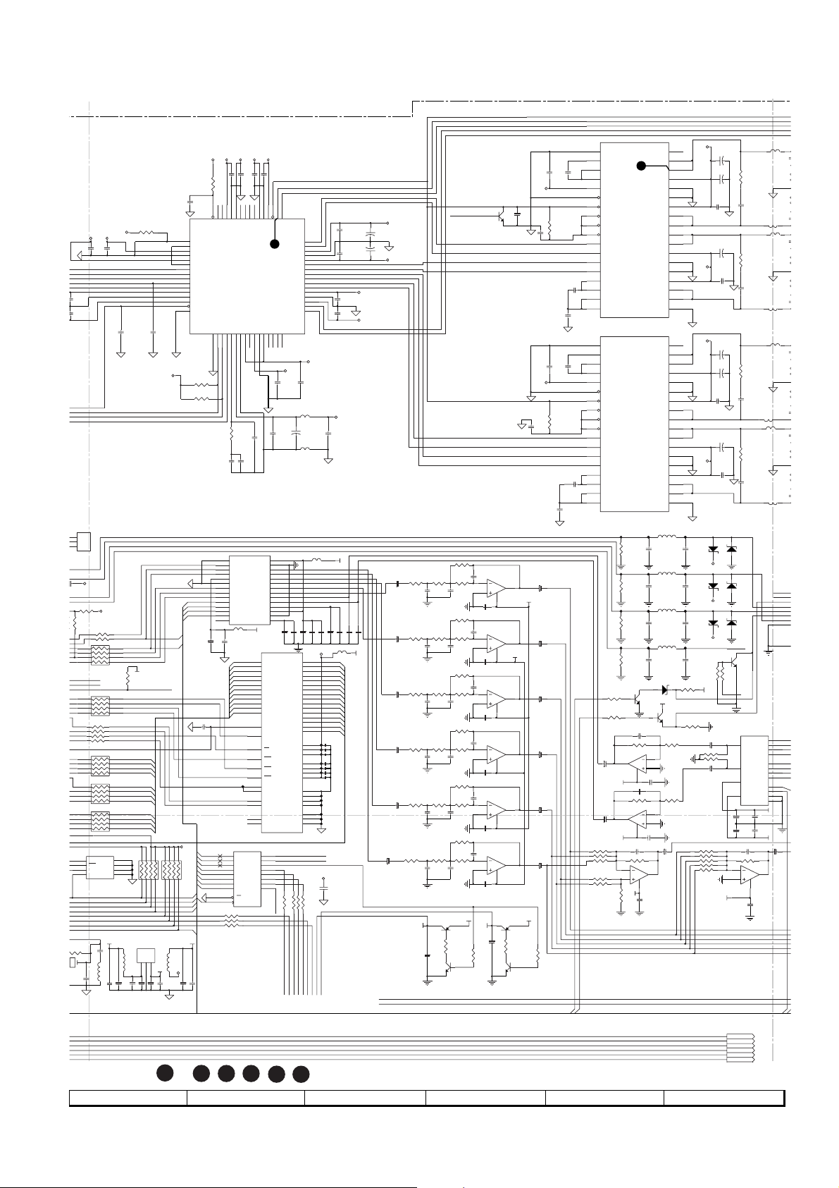
• The numbers 1 to 5 , 10 , 11 , 13 , 14 are waveform numbers shown in page 36, 37.
7
8 9 10 11 12
Figure 15 SCHEMATIC DIAGRAM (2/12)
– 15 –
TCLOSE-SW
TOPEN-SW
LSW
TRAY-REV
TRAY-FWD
DMUTE
TCLOSE-SW
TOPEN-SW
LSW
TRAY-REV
TRAY-FWD
DMUTE
Page 16
HT-CN400DVH/HT-CN400DVE/HT-CN500DVH/HT-CN500DVE
VREF
107
C136 104
3
0
0
2
3
3
C
3
L
L
IMP809SEUR
HIRQB
0
0
0
C
4
P
K
K
SITUATION :
YUV7CAMYUV3
1
2
3
TWS/SEL_PLL2
TSD0/SEL_PLL0
TSD1/SEL_PLL1
4
PCLK2XSCN/CAMYUV4
PCLKQSCN/CAMYUV5/AUX3[2]
VSSCN/CAMYUV6/EAUX3[1]
HSSCN/CAMYUV7/EAUX3[0]
DBANK0/DRAS1
DBANK1/DRAS2
11
SPDIF/SEL_PLL3
NC/APLL
VSS
VSS
VSS
41
48
192
200
208
R116
4.7K
R81 5.6K
R82 5.6K
IC809
LM358MX
LOW POWER
DUAL OPE AMP.
C892
104
DGND
AGND
WO
SREF
YUV1/VREF
YUV2/CDAC
YUV3/COMP
YUV4/RSET
AVSS(VDAC)
YUV5/YDAC
YUV6/VDAC
TDMTSC
MCLK
DSCK/DOE
DRAS0
DMA0
DMA1
DMA2
DMA3
DMA4
DMA5
DMA6
DMA7
DMA8
DMA9
DMA10
DMA11
XOUT
SPDIFOSPDIFIN
DGND
C843 56PF
R842 39K
AGND
RBCK
RWS
RSD
TBCK
TSD2
TSD3
DCAS
DWE
DCS1
DCS0
DQM
DSCK
DB0
DB1
DB2
DB3
DB4
DB5
DB6
DB7
DB8
DB9
DB10
DB11
DB12
DB13
DB14
DB15
AUX0
AUX1
AUX2
AUX3
AUX4
AUX5
AUX6
AUX7
XIN
CLK
C844 102
108
109
110
112
113
114
115
47
46
OK_DA
45
31
39
40
32
33
36
37
38
116
117
118
119
69
70
71
72
73
74
97
100
101
102
DMA0
53
DMA1
54
DMA2
55
DMA3
56
DMA4
57
DMA5
58
DMA6
61
DMA7
62
DMA8
63
DMA9
64
DMA10
65
DMA11
66
DB0
77
DB1
78
DB2
79
DB3
80
DB4
81
DB5
82
DB6
85
DB7
86
DB8
87
DB9
88
DB10
89
DB11
90
DB12
93
DB13
94
DB14
95
96
DB15
160
AUX0
161
AUX1
162
VFD-DA
165
166
RDS-DI
167
YU-D
168
SD
169
HWAITB
49
R113 33 OHM
50
R114 33 OHM
105
C893 102
R83 4.7K R84 10K
4
123
678
5
C845 152
C847 102
C846 561
C848 561
AGND
R104
10
S8V
5DAC
5
60 OHM at 100MHz
DGND
C894
104
270 OHM
MCLK
TBCK
TWS
TSD0
TSD1
TSD2
R112
C138
10UF 104
R109
0 OHM
B5V
R85
4.7K
104
C137
VCC3
R105
OPEN
R107 4.7K
R106 4.7K
R108 4.7K
R110
R111
RA1
1
2
3
4
ENCODE1
ENCODE2
RA1
4
3
2
1
R160
R161
R162
R163
RA1
4
3
2
1
RA1
4
3
2
1
RA1
4
3
2
1
8
VCC
7
WC
6
SCL
5
SDA
C139
CLK
R115 56K
22PF
C140
R86
18K
ADJV
ADRREC
ADPH
ADBH
ADTE
ADFE
XL101
27MHz
D801 1N4148
C849
RFP
471
C850
RFN
471
R870 100
R871 4.7
BHC
WO
TEC
TSTD1
TSTD0
FC
BST
TBAL
FBAL
SGC
SLDO
SPDO
TDO
FDO
R2A[0..8]
TA2
C141
C895
103
I
EE
22PF
HIRQB
LWRHL
LWRHL
A
LOE#
B
HD[0..7]
DCI_ERR
HCLK#
HDACK#
DCI_REQ
DCI_FDS
C
EAUX40
TDMDR
TDMCLK
TDMFS
LCS1#
HIRQB
FGO
RESB
GU
VCC
LOE#
C101
104
IC101
SST39VF080
MULTI-PURPOSE FLASH
HD[0..7]
DCI_ERR
HCLK#
HDACK#
DCI_REQ
DCI_FDS
EAUX40
TDMDR
TDMCLK
TDMFS
LCS1#
HIRQB
FGO
RESB
GU
C102
10UF
A16
1
A15
2
A14
3
A13
4
A12
5
A11
6
A9
7
A8
8
WRLL#
9
10
11
12
A18
13
A7
14
A6
15
A5
16
17
A4
18
A3
19
A2
20
A1
72CE
72CLK
72DA
DVD
S-B
S-A
S-BLNK
S-SWTCH
VCC
C104
104
VFDCE
VFDCLK
LMUTE
MUTE
2259DA
2259CL
WM8739CE
DOUT
BICK
LRCK
A16
A15
A14
A13
A12
A11
A9
A8
WE#
NC
NC
NC
A18
A7
A6
A5
A4
A3
A2
A1 A0
D
QUAD 2:1 MULTIPLEXER
TCLOSE-SW
TOPEN-SW
R829 100 OHM
R830 100 OHM
R832 100 OHM
CN801
DRP
5
DRM
FROM DVD
MECHANISM UNIT
with LOADING
MOTOR PWB (210)
FROM
DVD
MECHANISM UNIT
with SPIN/SLED
MOTOR PWB (210)
FROM
DVD
MECHANISM UNIT
with PICKUP
PWB (210)
4
3
2
1
R801 4.7K
R802 4.7K
D3V
R803
4.7K
CN802
SLD-F
1
SLD-F
SLD-R
2
SLD-R
SP+
3
LSW
SP-
4
LSW
5
SPDP
DGND
6
SPDM
CN803
FCS-R
1
F-
TRK-D
2
F+
TRK-R
3
T+
FCS-D
4
T-
R8117 1K
5
C
R8118 1K
6
D
7
CD/DVD
8
R
R8119 1K
9
A
R8120 1K
10
B
11
R850 10K
F
12
GND-P
13
V
14
VC
15
R851 10K
E
16
NC
17
VR-CD
18
VR-DVD
19
LD-CD
20
LDS
MD
21
HFM
22
L801
601
NC
23
LD-DVD
24
GND-LD
25
26
Q801
KTA1505
AGND
C817
R816
R843
18 OHM
18 OHM
C818
102
AGND
E
F
G
H
TRAY-REV
TRAY-FWD
DRP
DRM
FCS-D
TRK-R
FCS-R
TRK-D
SP+
SP-
SLD-F
SLD-R
IC801
LA6560
MOTOR
DRIVER
R807
10K
PREF
AGND
C812
104
C813
47UF
C888 2PF
C889 2PF
C890
2PF
AGND
AGND
C816
102
Q802
KTA1505
10UF
R844 18 OHM
R818 1 8 OHM
IC101
2
5
6
9
12
15
16
19
IC102
74F374D
2
5
6
9
12
15
16
19
IC103
74HC374
2
3
5
6
11
10
14
13
1
15
SN74F157A
S8V
T4T3
FWD
REV
C800
104
C831 104
C803
47UF
C805
104
R806 22K
RF5V
C814
104
C815
47UF
C833
C820
102
10UF
C819
IC103
1A
1B
2A
2B
3A
3B
4A
4B
A/B
G
IC104
471
IC102
IC103
GND
DQ7
DQ6
DQ5
DQ4
VCC
VCC
DQ3
DQ2
DQ1
DQ0
GND
TSTD0
A17
A19
A10
OE#
CE#
NC
NC
IC104
TSTD1
RESET 2.93V
40
A17
39
38
37
A19
36
A10
D7
35
D6
34
33
D5
32
D4
31
30
29
28
D3
27
D2
26
D1
25
D0
LOE#
24
23
LCS3#
22
21
A0
D03Q0
D14Q1
D27Q2
D38Q3
D413Q4
D514Q5
D617Q6
D718Q7
OE
CLK
D03Q0
D14Q1
D27Q2
D38Q3
D413Q4
D514Q5
D617Q6
D718Q7
OE
CLK
1Y
2Y
3Y
4Y
1
2
3
4
5
6
7
8
9
10
11
12
13
14
15
16
17
18
SLDO
C891
2PF
AGND
KTC3875
AGND
R820
4.7K
LDD1
LDD2
VC33
D0
D1
D2
D3
D4
D5
D6
D7
1
11
D8
D9
D10
D11
D15TUPO
D14
D13
D12
1
11
DMDR
4
DMCLK
7
DMFS
9
VCC
12
R815 22K
FWD
S-GND
REV
VCONT
VCC2
MUTE1
VLO-
VLO+
VO4+
VIN4+
VO4-
VREF-IN
VO3+
VIN1-SW
VO3-
VREF-OUT
FR37FR
VO2+
REG-OUT
VO2-
REG-IN
VIN3+
VO1+
VO1-
VCC1
VIN2+
VIN1
VIN1-A
VIN1+A
VIN1-B
VIN1+B
R826 8.2K
R827 8.2K
R828 8.2K
R831 8.2K
R834 47K
R835 1.2M
R836 47K
R837 2.2M
R838 47K
R839 47K
R840 820K
R845 22K
R846 2.2M
R847 22K
R848 820K
R849 1.2M
R825
Q805
3.3K
Q803
KTC3875
R821
10K
AGND
C103 104
VC33
LCS2#
VCC
C105
104
R150 33 OHM
R151 33 OHM
R152 33 OHM
C106
104
36
35
34
33
VIN4
32
VIN4
31
30
29
28
38
27
26
25
24
VIN3
23
VIN3
22
21
VIN2
20
VIN2
19
R822
10K
LCS0#
173
LCS1#
LCS2#
LCS3#
WRLL#
LWRHL
LOE#
R169
4.7K
R168
4.7K
D5V
R813 3.6K
C809
104
DGND
R808
27K
C822 56PF
C824 56PF
Q806
KTC3875
AGND
R823
10K
LCS0
174
LCS1
175
LCS2
176
LCS3
198
LWRLL
199
LWRHL
170
LOE
A0
204
LA0
A1
205
LA1
A2
206
LA2
A3
207
LA3
A4
2
LA4
A5
3
LA5
A6
4
LA6
A7
5
LA7
A8
6
LA8
A9
7
LA9
A10
10
LA10
A11
11
LA11
A12
12
LA12
A13
13
LA13
A14
14
LA14
A15
15
LA15
A16
16
LA16
A17
19
LA17
A18
20
LA18
A19
21
LA19
22
LA20
A21
23
LA21
D0
178
LD0
D1
179
LD1
D2
180
LD2
D3
181
LD3
D4
182
LD4
D5
185
LD5
D6
186
LD6
D7
187
LD7
D8
188
LD8
D9
189
LD9
D10
190
LD10
D11
191
LD11
D12
194
LD12
D13
195
LD13
D14
196
LD14
D15
197
LD15
142
DCI_REQ
HWRQ/DCI_REQ/EAUX4[1]
EAUX4[0]
143
HRDQ/EAUX4[0]
144
DCI_ERR
HIRQ/DCI_ERR/EAUX4[7]
145
AVIN1
HRST/EAUX3[5]
146
DMUTE
HIORDY/EAUX3[3]
DCLK
149
HWR/DCI_CLK/EAUX4[5]
HDACK#
150
HRD/DCI_ACK/EAUX4[6]
GU
151
HIOCS16/CAMPCLK/EAUX3[4]
152
TRAY-FWD
HCS1FX/EAUX3[7]
TRAY-REV
153
HCS3FX/EAUX3[6]
LSW
154
HA0/EAUX4[2]
TOPEN-SW
155
HA1/EAUX4[3]
TCLOSE-SW
158
HA2/EAUX4[4]
122
HD0
HD0/DCI[0]/EAUX1[0]
123
HD1
HD1/DCI[1]/EAUX1[1]
124
HD2
HD2/DCI[2]/EAUX1[2]
125
HD3
HD3/DCI[3]/EAUX1[3]
HD4
126
HD4/DCI[4]/EAUX1[4]
HD5
127
HD5/DCI[5]/EAUX1[5]
HD6
128
HD6/DCI[6]/EAUX1[6]
HD7
131
HD7/DCI[7]/EAUX1[7]
DCI_FDS
132
HD8/DCI_FDS/EAUX2[0]
TE_BIAS EARDEC
133
HD9/EAUX2[1]
RESB
134
HD10/EAUX2[2]
AVIN2
135
HD11/EAUX2[3]
HIRQB
136
HD12/EAUX2[4]
WRQ_INT
137
HD13/EAUX2[5]
FGO
140
HD14/EAUX2[6]
IR
141
HD15/EAUX2[7]
28
TDMDR
29
TDMCLK
30
TDMFS
C1011 22PF
C1010 22PF
C1009 22PF
R814
10K
DMUTE
R812
MWEB
10K
MRAS1B
SREF
C810
TDO
47UF
R2A[0..8]
15K
R810 10K
FDO
R809 10K
SPDO
C839
3P
R868
R841
3.3K
3.3K
C840
56PF
PREF
RF5V
1
CAP
2
VCC
3
C821 56PF
C823 56PF
KTC3875
AGND
Q804
PDRF
4
PD1
5
PD2
6
PD3
7
PD4
8
GND
9
FIN1
10
FIN2
11
PIN1
12
PIN2
13
TIN1
14
TIN2
15
LDD1
16
LDS1
LDD1
LDS
AVCC(PL
AVCC(VDA
TDMDX/RSE
NC/CAMVS
CAMYUV0
CAMYUV1
42
202
203
D3V
1
2
R2IO0
3
R2IO1
4
R2IO2
5
R2IO3
6
7
R2IO4
8
R2IO5
9
R2IO6
10
R2IO7
11
12
13
14
15
16
R2A0
17
R2A1
18
R2A2
19
R2A3
20
T5
R866 22K
C837
100UF
R1
1K
64
63
62
60
59
57
56
55
54
53
52
RFP61N/C
N/C
RFN
VCC
CAN
CAO
GND
PREF58FSET
RFOP
RFON
12
IC802
LA9703W
DVD PLAYERS RF AMP.
LDD217LDS218GND19LDTH20LDON121LDON222AGOF23BCA24GU25DVD/CD26DPD/TE27WO/PP28VCC29TH30XHTR31SGC
RF3V
AGND
C864
GU
LDON2
LDON1
DVD-CDB
VC3VC3VC3VC3VC3VC3VC3VC3VC3VC3VC3VC3VC3VC
VC
VC3VC
IC106
ES6028
MICROCOMPUTER
VSS8VSS17VSS
VSS
VSS
AVSS(PLL)52VSS60VSS67VSS76VSS84VSS
26
34
43
C867 47UF
VSS
VCC
DQ15
DQ0
DQ14
DQ1
DQ13
DQ2
DQ12
DQ3
VSS
VCC
DQ11
DQ4
DQ10
DQ5
DQ9
DQ6
DQ8
DQ7
NC
NC
LCAS
NC
UCAS
WE
OE
RAS
IC804
DRAM
A8
NC
A7
A0
IC41LV16256
A6
A1
A5
A2
A4
A3
VSS
VCC
SREF
C835
C838
100UF
104
R865 8.2K
R864 36K
51
50
49
AGND
LPC
PHC
SREF
BCAI
48
SREFI
47
PH
46
BH
45
ISET
44
WOC
43
PPN
42
PP
41
WO
40
TE
39
FE
38
RREC
37
CP
36
TEBL
35
FEBL
34
FC
33
BST
32
101
AGND
91
40
39
38
37
36
35
34
33
32
31
30
29
28
27
26
25
24
23
22
21
DGND
C836
C834
1UF
104
C830
472
C829 472
RF3V
C827 473
VSS
VSS98VSS
VSS
VSS
129
103
120
138
R2IO[0..15]
R2IO15
R2IO14
R2IO13
R2IO12
R2IO11
R2IO10
R2IO9
R2IO8
PREFPREF
C832
47UF
SREF
R863 33K
R861 6.8K
R860 6.8K
R859 6.8K
R857 10K
C826 472
TBAL
FBAL
FC
BST
SGC
XHTR
DEFECTO
147
VSS
156
VSS
VSS
163
R862 33K
C828 1UF
VC2VC2VC2VC2VC2VC2VC
VSS
VSS
VSS
171
177
184
MCASLB
MCASUB
MOEB
R2A8
R2A7
R2A6
R2A5
R2A4
R858 62K
R856 6.8K
R855 6.8K
R854 10K
R853 33K
C825 101
R852 5.6K
• NOTES ON SCHEMATIC DIAGRAM can be found on page 11.
1
23456
Figure 16 SCHEMATIC DIAGRAM (3/12)
– 16 –
Page 17
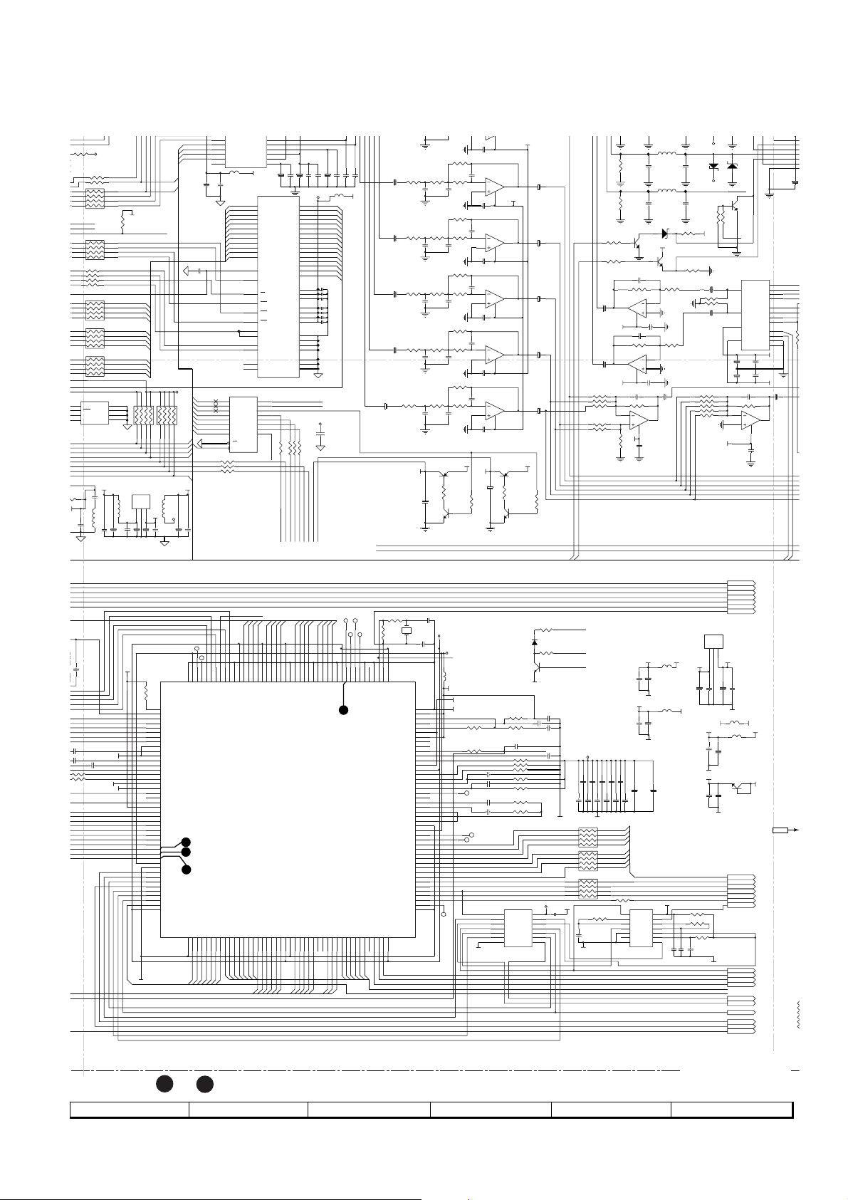
HT-CN400DVH/HT-CN400DVE/HT-CN500DVH/HT-CN500DVE
103
DIN2
VOUT1L
D801 1N4148
z
R498 6 8K
R105
VC33
OPEN
R110 33 OHM AMCLK
R111 33 OHM
RA101 33x4
18
27
36
45
R174
E1
4.4K
E2
RA102 33x4
45
36
27
18
R160
33 OHM
R161
33 OHM
R162
33 OHM
R163
33 OHM
RA104 10x4
45
36
27
18
RA105 10x4
45
36
27
18
RA106 10x4
45
36
27
18
DB[0..15]
VCC
WC
SCL
IC107
TA24C02N
EEP ROM
C141
22PF
1
S0
2
S1
3
S2
GND4SDA
RA117
4.7Kx4
VC33
L101 10uH C142 102
C1005
C1006
10UF
104
8
7
6
5
56K
BICK
LRCK
SD0
SD1
SD2
VC33
VIDEO_SW
MA0
MA1
MA2
MA3
MA4
MA5
MA6
MA7
MA8
MA9
MA10
MA11
MA[0..11]
18
27
36
45
18
27
IC114
RT9164
FB102
100 OHM
+5V_1
123
C1001
104
C1003
C1002
C1004
10UF
10UF
104
9
DOUT
10
72CE
11
72CLK
12
72DA
13
14
FB115
104
C151 10UF
C152
C100
10PF
RCLK
CKE
CS0#
RAS0#
CAS#
WE#
DQMX
BANK0
BANK1
IC109
4MX16Y3VTW
DRAM
C199
+5V
104
74HC374
3
4
7
8
13
D1
14
D2
17D0D3
D4
1
LCS1#
11
R119 33 OHM
R120 33 OHM
R121 33 OHM
VCC
RA118
4.7Kx4
36
45
FB101
100 OHM
VCC
C1000
10UF
DIN3
DOUT
ML/I2S
VMID
MC/IWL
VREFP
MD/DM
VREFN
MUTE REFADC
601
VCC
23
MA0
24
MA1
25
MA2
26
MA3
MA4
29
MA5
30
31
MA6
MA7
32
MA8
33
MA9
34
MA10
22
MA11
35
38
37
18
17
16
15
39
20
21
36
40
IC108
D0 Q0
D1 Q1
D2 Q2
D3 Q3
D4 Q4
D5 Q5
D6 Q6
D718Q7
OE
CLK
20
AINL
19
AINR
18
17
16
15
A0
A1
A2
A3
A4
A5
A6
A7
A8A9DQ8
A10
A11
CLK
CKE
IC109
CS19VCC
RAS
CAS
WE
DQML
DQMH
BA0
BA1
NC
NC
2
5
6
9
12
15
16
19
SW1_VIDEO
C153 10UF
C154 104
DQ0
DQ1
DQ2
DQ3
DQ4
DQ5
DQ6
DQ7
DQ9
DQ10
DQ11
DQ12
DQ13
DQ14
DQ15
VCC
VCC
VCCQ
VCCQ
VCCQ
VCCQ
VSSQ
VSSQ
VSSQ
VSSQ
VSS
VSS
VSS
R122 33 OHM
R123 33 OHM
SYR
RDS-DATA
TU-CE
33 OHM
R124
TU-DI
103
104
104
104
104
C155 10UF
TUPO
TU-CL
33 OHM
R125
YU-DO
C160
C156 104
C157 10UF
C158
C159
FB116
VCC33
601
2
DB0
4
DB1
5
DB2
7
DB3
8
DB4
10
DB5
11
DB6
13
DB7
42
DB8
44
DB9
45
DB10
47
DB11
48
DB12
50
DB13
51
DB14
53
DB15
1
C144
14
C145
27
C146
3
C147
9
C148
43
C149
49
C144-C150(104)
C150
6
12
46
52
28
41
54
VCC
C143
104
SDB
TU5V
TU12V
C402
10UF
R405 1K
R-A
C161
VC33
C403
10UF
SL-A
R409 1K
C404
10UF
R413 1K
SR-A
C405
10UF
C-A
R417 1K
C406
R421 1K
SUB-A
10UF
TU-R
TU-L
R408 22K
R406 4.7K
C412
C411
103
103
R412 22K
R410 4.7K
C416
C415
103
103
R416
R414 4.7K
C420
C419
103
103
R420 22K
R418 4.7K
C424
C423
103
103
R424 5.6K
R422 4.7K
C428
C427
103
103
Q104
A733
TU5V
R138
4.7K
C197
100UF
Q103
C945
R407 1K
R411 1K
R415
R419 1K
R423 1K
4
IC401B
6
5
IC402A
2
3
IC402B
6
5
IC403A
2
3
IC403B
6
5
100UF
C198
-12V
C433
10UF
7
8
+12V
C434
10UF
1
4
C435
10UF
7
8
C436
10UF
1
4
C437
10UF
7
8
Q106
+12V+5V
A733
R140
4.7K
R139
10K
Q105
C945
R425 47K
R426 68K
R491 68K
R427 360K
R428 360K
S-SWTCH
S-BLNK
IC401~404/IC406
R131
R132
C459
10UF
C461
10UF
R429
56K
RC4558D
L104 2.4UH
YDAC YG
R129
C178
75 OHM
471
L105 2.4UH
VDAC
R130
C180
75 OHM
471
ZD109
C458
R462 10K
IC406A
1
4
C460 47PF
R464 10K
IC406B
7
8
C438 47PF
R430
6
5
8
+12V
Q101
C945
47PF
C462 104
C463 104
33K
IC404B
C443
104
7V
VCC
Q102
C945
R461
2
3
R463
1K
6
5
C439
10UF
7
4.7K
4.7K
-12V
+12V
R133
1K
C179
471
VCC33E
CVBS
C181
471
1K
+12V(IN)
R134
75 OHM
C456 10UF
R459 100K
R460 100K
C457 10UF
R431 47K
R432 68K
R433 68K
R434 68K
R492 68K
VCC33E
ZD1057VZD106
R167
10K
R166 10K
DVD
4CH MULTIPLEXER
13
16
-12V
C410
104
C413
151
C414
104
C417
151
C418
104
22K
C421
151
1K
C422
104
C425
151
C426
104
C429
332
C430
104
TU12V
R137
10K
7V
CVBS1
Q108
C945
IC405
TC4052BFN
X
3
Y
VDD
7
VEE
C453
100UF
C455
100UF
C440 47PF
R435 33K
2
3
4
C444
104
X0
X1
X2
X3
Y0
Y1
Y2
Y3
A
B
INH
GND
C452
104
C454
104
1
IC404A
CVBS1
12
14
15
11
1
5
2
4
10
9
6
8
R497 6.8K
+7V
S-B
S-A
-7V
C441
10UF
TCLOSE-SW
TCLOSE-SW
TOPEN-SW
TOPEN-SW
LSW
LSW
TRAY-REV
TRAY-REV
TRAY-FWD
TRAY-FWD
DMUTE
A3V
C955 47UF
100 OHM
R8109
330 OHM
C81
221
OSCIN
C954A 104
C957 104
AGND
D2V
C959 104
HD[0..7
DCI_ERR
DCI_FDS
DCLK
HDACK#
DCI_REQ
LWRHL
DGND
LOE#
TDMFS
TDMCLK
TDMDR
HWAITB
HIRQB
LCS1#
FGO
RESB
GU
DMUTE
OSCIN
IC810
RT9164
123
D5V
C952A 104
C953A 47UF
DGND
FB901
601
D3VA3V
A3VRF3V
601
FB902
C956A 47UF
Q903A
C945
D3V
C958 47UF
DGND
RB904
FROM
POWER PWB
P25 12-D
HD[0..7]
DCI_ERR
DCI_FDS
DCLK
HDACK#
DCI_REQ
LWRHL
LOE#
TDMFS
TDMCLK
TDMDR
HWAITB
HIRQB
LCS1#
FGO
RESB
GU
DVD-CDB
LDON1
LDON2
DEFECTO
XHTR
T20
C895
103
C
C849
471
C850
471
BHC
WO
TEC
TSTD1
TSTD0
FC
BST
TBAL
FBAL
SGC
SLDO
SPDO
TDO
FDO
A[0..8]
SREF
R8116
6.8K
1
2
AD0
3
4
5
6
7
8
9
10
FGO
INT_DEC
RDY
WR
11
12
13
14
15
16
17
18
19
20
21
22
23
24
25
26
27
28
29
30
31
32
33
34
35
36
37
38
39
RESB
40
RD
41
42
43
44
LCS1#
D8
DGND
DGND
C851
104
100K
4.7K
D3V
AGND
AD1
AD0
JV
RREC
RF-PH
RF-BH
TE
FE
TEST0
EFMINP
TEST1
EFMINN
SLCLPFO
SLCLPFI
SLC01
SLC02
AVDD1
AVSS
BHC
WO
TEC
VREF
TSTD1
TSTD0
F0
BST
TBAL
FBAL
SGC
SLDO
SPDO
TDO
FDO
DVDD0
DVSS
FG
HIRQB
HWAITB
HRESB
HRDB
HWRB
HCSB
HDAT0
DVDD1
176
7
8
6
174
175
DVSS
HFLIO
DVDD0
DVSS45HDAT146HDAT2
47
D9
D10
WRQ_INT
R2IO0
R2IO6
R2IO7
T19
165
166
167
168
169
173
TESIO
HDAT348HDAT449HDAT550HDAT651HDAT752HADR053HADR154HADR255HADR356HADR457HADR558HADR659MA062MA163MA264MA365MA468MA569MA670MA771MA872MA973MA1074HADR778HADR879HADR980HADR1081HADR1182HADR12
D11
172
RFP3
D12
170
171
RFP1
RFP2
D13
D14
RFP0
DVSS
DEFECTI
DEFECTO
A1A2A3A4A5A6A7
D15
DVDD1
163
164
MD6
MD7
R2IO15
R2IO4
R2IO5
R2IO2
R2IO1
R2IO3
R2IO14
154
155
160
152
153
156
157
158
159
161
162
MD0
MD1
MD2
MD3
MD4
MD5
DVSS
MD15
DVDD3
DVDD3
IC803
LC78663NRW
DVD FRONT END
MWEB60MRAS1B61DVDD366DVSS67MOEB75MCASUB76MCASLB77C2F84ROMXA85ROMCK86LRSY87DVDD1
R2A2
R2A4
R2A0
R2A1
R2A5
R2A3
MWEB
MRAS1B
T15
T13
T14
R2IO11
148
T12
R2IO9
R2IO8
R2IO10
139
140
141
142
143
144
145
146
147
FSX
MD 8
MD 9
EFLG
DVSS
MD1 0
MD1 1
DOUT
DVDD1
DVDCKIO
9
A8A9A10
A11
A12
MOEB
MCASUB
MCASLB
R2IO12
R2IO13
149
150
151
DVSS
MD1 2
MD1 3
MD1 4
R2A8
R2A6
R2A7
137
138
TEST2
83
A13
X16MIO
135
136
DVSS
XOUT
R891 330OHM
R890
1M
133
134
XIN
DVDD2
DVDD0
VCOC
VRPFR
VPDO
AVDD3
JVRVO
JVAIN
JVAO
JVCPC
JVCPI
AVDD2
DVDFR
FISET
PISET
FPDO
PPDO
VCOCTL
DVDD0
EFMOUT
AVD7
AVD6
AVD5
AVD4
AVD3
AVD2
AVD1
AVD0
AVERRB
AVSCTB
AVDACK
AVACKO
AVREQI
EMPH
88
DVSS
AVSS
AVSS
CDFR
PCN
LF3
LF2
LF1
DVSS
PCK
DVSS
XL801
16.9344MHz
C866
C865
10PF
D3V
10PF
D2V
L802
601
A2.5V
AGND
132
DGND
131
130
129
R887 10K
128
127
126
125
124
R883 6.8K
123
122
121
120
119
118
117
116
115
114
113
112
111
110
109
108
107
106
105
104
103
102
101
100
99
98
97
96
95
94
93
92
91
90
89
C859 104
C858
T11
C856 104
C855 104
T10
T9
AVERRB#
AVSCTB
AVDACK#
AVDENB#
AVREQI
INT_DEC
T8
RD
IC807
SN74LVC32ANS
QUAD 2-1/P OR GATE
220 OHM
104
AVD7
AVD6
AVD5
AVD4
AVD3
AVD2
AVD1
AVD0
1
2
3
4
5
6
D901
1N4148
R889 5.6K
R888
C861
R882 10K
R881 1.2K
R880 1.8K
R879 22K
R878 22K
R876 1.2K
R875
A1
B1
Y1
A2
B2
Y2
VSS7Y3
R894 68K
AGND
C863 104
561
ADJV
680 OHM
VCC
B4
A4
Y4
B3
A3
R893
Q904A
C945
C854 104
C862 104
C860 103
D3V
14
13
12
11
10
9
8
10K
C896
104
LCS1#
RDY
ADTE
DEFECTO
TE_BIAS
D3V
C875 104
C881 104
C877 104
C879 104
C880 104
C878 104
C874 104
C876 104
DGNDAGND
RA801 10x4
18
27
36
45
18
27
36
45
RA802 10x4
RA803 10x4
18
27
36
45
DGND
R873 10 OHM
100 OHM
R8106
C897
151
DGNDDGND
C883 104
C884 104
C882 104
HD7
HD6
HD5
HD4
HD3
HD2
HD1
HD0
1
2
3
4
5
6
SN74HC14NS
INVERTER
C961 104
RF5V
C951A 104
C885 47UF
I1
O1
I2
O2
I3
O3
VSS7O4
IC808
MGND
AGND
VCC
D5V S5V
FB903
601
C960 47UF
FB904
601
C950A 47UF
C887 47UF
D3V
14
13
I6
12
O6
11
I5
10
O5
9
I4
8
C898
104
D5V
R8115 10K
R8113
C899
151
• The numbers 1 to 12 are waveform numbers shown in page 36, 37.
7
8 9 10 11 12
Figure 17 SCHEMATIC DIAGRAM (4/12)
– 17 –
Page 18
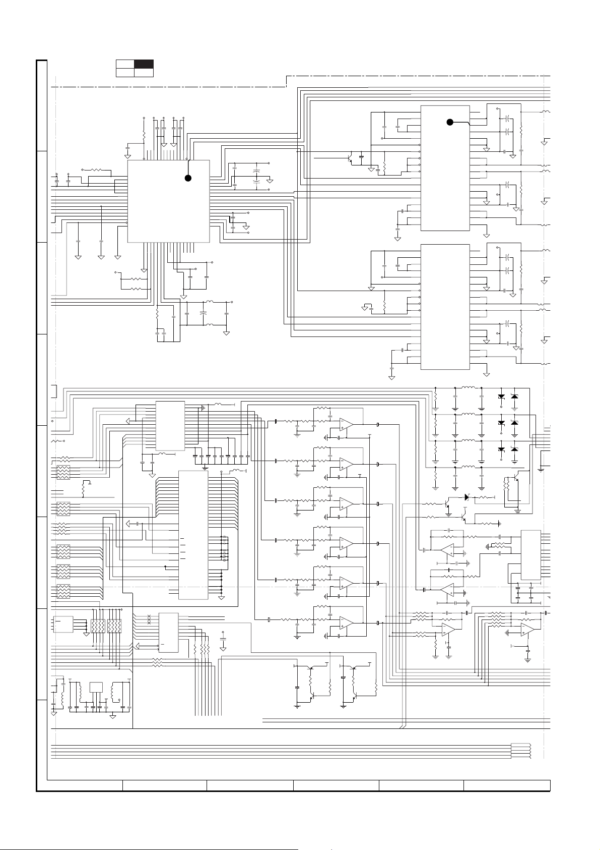
HT-CN400DVH/HT-CN400DVE/HT-CN500DVH/HT-CN500DVE
1
C
1
R
1
R
3
5
1
0
R
R
u
S
O
C141
R
4
SITUATION :
OUT1_A
OUT1_B
OUT6_A
OUT6_B
A
+2.5V
B
C
D
15
164-CG
VCC33E
05
EN
110 33 OHM AMCLK
111 33 OHM
E
0
1
2
3
F
VCC
WC
SCL
TA24C02N
EEP ROM
G
22PF
C512
104
RA101 33x4
RA102 33x4
RA104 10x4
RA105 10x4
RA106 10x4
IC107
+3.3V
VC33
33 OHM
33 OHM
33 OHM
33 OHM
GND4SDA
L101 10uH C142 102
C1006
+2.5V
C513
104
8
7
6
5
R174
4.4K
5
6
7
8
5
6
7
8
5
6
7
8
5
6
7
8
DB[0..15]
1
S0
2
S1
3
S2
VC33
C1005
10UF
104
NS
R523
C599
C591
47PF
102
+3.3V
BICK
LRCK
SD0
SD1
SD2
VC33
VIDEO_SW
MA0
MA1
MA2
MA3
MA4
MA5
MA6
MA7
MA8
MA9
MA10
MA11
MA[0..11]
18
27
36
45
18
RA117
4.7Kx4
IC114
RT9164
FB102
100 OHM
+5V_1
123
C1001
104
C1003
C1002
C1004
10UF
10UF
104
+3.3V
+2.5V +3.3V
R526
47K
C590
102
61515657586255535264546359
PWDN
SDO_56
SDO_78
1
MVO
2
TEST_MODE
3
VDD3.3_1
4
GND_1
5
VDD2.5_1
6
SDI_78
7
SDI_56
8
SDI_34
9
SDI_12
AUDIO PROCESSOR
10
LRCKI
11
BICKI
12
VDD3.3_2
13
GND_2
14
VDD2.5_2
15
RESET
16
PLL_BYPASS
SDA
SCL
SA
181917282027222123252632313029
10K
R503
10K
R502
R527
3.3K
C600
1200PF
1
2
3
4
5
6
7
8
9
DOUT
10
72CE
11
72CLK
12
72DA
13
14
FB115
104
C151 10UF
C152
C100
10PF
IC109
4MX16Y3VTW
DRAM
VCC
3
4
RA118
7
4.7Kx4
8
13
D1
14
D2
17D0D3
27
D4
36
45
FB101
100 OHM
VCC
C1000
10UF
C199
104
+5V
1
LCS1#
11
R119 33 OHM
R120 33 OHM
R121 33 OHM
+2.5V +3.3V
104
104
C515 104
C516
C514
60
BICKO
GND_7
LRCKO
SDO_12
SDO_34
VDD2.5_6
VDD2.5_7
VDD3.3_7
IC503
STA308
XTI
GND_3
VDDA_PLL
PLL_FILTER
GNDA_PLL
CKOUT
VDD2.5_3
VDD3.3_PLL
24
C601
100PF
C602
100PF
GNDA
IC110
WM8772
6CH D/A 2CH A/D
AVDD
MODE
AGND
MCLK
OUT3R
BCLK
OUT3L
LRCK
OUT2R
DVDD
DGND
OUT2L
DIN1
OUT1R
DIN2
VOUT1L
DIN3
AINL
DOUT
AINR
ML/I2S
VMID
MC/IWL
VREFP
MD/DM
VREFN
MUTE REFADC
601
VCC
23
MA0
24
MA1
25
MA2
26
MA3
29
MA4
30
MA5
31
MA6
MA7
32
MA8
33
MA9
34
MA10
22
MA11
35
38
RCLK
37
CKE
CS0#
RAS0#
18
CAS#
17
16
WE#
15
DQMX
39
BANK0
20
BANK1
21
36
40
IC108
74HC374
D0 Q0
D1 Q1
D2 Q2
D3 Q3
D4 Q4
D5 Q5
D6 Q6
D718Q7
OE
CLK
104
C517
49
50
EAPD
GND_6
OUT1_A
OUT1_B
VDD3.3_6
13
VDD3.3_3
OUT7_A
OUT7_B
OUT8_A
OUT8_B
C544
104
VDDA
C603
22UF
C543
104
28
27
26
25
24
23
22
21
20
19
18
17
16
15
C153 10UF
A0
A1
A2
A3
A4
A5
A6
A7
A8A9DQ8
A10
A11
CLK
CKE
IC109
CS19VCC
RAS
CAS
WE
DQML
DQMH
BA0
BA1
NC
NC
2
5
6
9
12
15
16
19
SW1_VIDEO
R122 33 OHM
SYR
OUT2_A
OUT2_B
VDD2.5_5
GND_5
VDD3.3_5
OUT3_A
OUT3_B
OUT4_A
OUT4_B
OUT5_A
OUT5_B
VDD2.5_4
GND_4
VDD3.3_4
OUT6_A
OUT6_B
+2.5V
+
C154 104
DQ0
DQ1
DQ2
DQ3
DQ4
DQ5
DQ6
DQ7
DQ9
DQ10
DQ11
DQ12
DQ13
DQ14
DQ15
VCC
VCC
VCCQ
VCCQ
VCCQ
VCCQ
VSSQ
VSSQ
VSSQ
VSSQ
VSS
VSS
VSS
33 OHM
R123 33 OHM
R124
RDS-DATA
TU-CE
TU-DI
48
47
46
45
44
43
42
41
40
39
38
37
36
35
34
33
+3.3V
C545
104
601
L515
L514
FB114 601
C155 10UF
C156 104
2
4
5
7
8
10
11
13
42
44
45
47
48
50
51
53
1
14
27
3
9
43
49
6
12
46
52
28
41
54
TUPO
33 OHM
R125
TU-CL
YU-DO
SDB
601
VCC33
TU5V
EAPD
C634
SPK_MUTE
OUT2_A
OUT2_B
OUT3_A
OUT3_B
OUT5_A
OUT5_B
OUT4_A
OUT4_B
R404 22K
R402
4.7K
R403 1K
C408
C407
103
103
R408 22K
C413
151
R406 4.7K
R407 1K
C412
C411
103
103
R412 22K
C417
151
R410 4.7K
R411 1K
C416
C415
103
103
R416
C421
151
R414 4.7K
R415
C420
C419
103
103
R420 22K
C425
151
R418 4.7K
R419 1K
C424
C423
103
103
R424 5.6K
C429
332
R422 4.7K
R423 1K
C428
C427
103
103
Q104
A733
TU5V
R138
4.7K
C197
100UF
Q103
C945
+2.5V
+3.3V
104
C161
VC33
C144-C150(104)
+2.5V
+
C593
2.2UF
C592
+
2.2UF
+3.3V
C401
10UF
R401 1K
L-A
C402
10UF
R405 1K
R-A
C403
10UF
SL-A
R409 1K
C404
10UF
R413 1K
SR-A
C405
10UF
C-A
R417 1K
C406
R421 1K
SUB-A
10UF
TU-R
TU-L
C521
104
C520
104
C519
104
C518
104
+2.5V
C546
104
VCC
104
104
104
C157 10UF
C158
C159
C160
FB116
601
DB0
DB1
DB2
DB3
DB4
DB5
DB6
DB7
DB8
DB9
DB10
DB11
DB12
DB13
DB14
DB15
C144
C145
C146
C147
C148
C149
C150
VCC
C143
104
TU12V
Q605
C945
22UF
C409
IC401A
151
2
1
3
4
6
5
2
3
6
5
IC403A
2
3
IC403B
6
5
IC401B
8
IC402A
4
IC402B
8
4
8
100UF
C198
Q105
C945
-12V
7
+12V
1
7
1
7
+12V+5V
Q106
A733
R140
4.7K
R139
10K
C410
104
C414
104
C418
104
22K
1K
C422
104
C426
104
C430
104
TU12V
R137
10K
L506
*R506
*C595
*/R507
*C596
*R508
*C597
*R509
*C598
PRB
7V
PBR
7V
YG
7V
CVBS1
Q108
C945
IC405
TC4052BFN
13
X
3
Y
16
VDD
7
VEE
C453
100UF
C455
100UF
C440 47PF
R435 33K
2
3
C444
104
4
L504
L505
L518
L519
L516
X0
X1
X2
X3
Y0
Y1
Y2
Y3
A
B
INH
GND
C452
104
C454
104
1
IC404A
30uH
1
*R5
*R5
L507
30uH
C
*
*
3
C
*R
*
30uH
30
C
1
*R
*
L517
30uH
VIDE
CVB
12
14
15
11
1
5
2
4
10
9
6
8
+7V
-7V
C
10
+28V
19
GNDREF
20
GNDR1
21
C526
C523
104
+3.3V
R501
10K
C522
104
C528
104
C548
104
+3.3V
R504
10K
C547
104
C551
104
C432
10UF
C433
10UF
C434
10UF
C435
10UF
C436
10UF
C437
10UF
104
C525
104
C550
104
C549
104
S-SWTCH
S-BLNK
VREG1
22
VREG1
23
VL
24
CONFIG
25
PWRDN
26
TRI-STATE
27
FAULT
POWER AMP.
28
TWARN
29
INLA
30
INLB
31
INRA
32
INRB
33
VREG2
34
VREG2
35
VSIG
36
VSIG
19
20
GNDR1
21
VREG1
22
VREG1
23
VL
24
CONFIG
25
PWRDN
26
27
FAULT
28
TWARN
29
POWER AMP.
INLA
30
INLB
31
INRA
32
INRB
33
VREG2
34
VREG2
35
VSIG
36
VSIG
4.7K
R131
R132
C459
10UF
-12V
C461
10UF
+12V
R425 47K
R426 68K
R491 68K
R427 360K
R428 360K
R429
56K
IC401~404/IC406
RC4558D
IC501
STA505
IC502
STA505
UDAC
R127
75 OHM
CDAC
R128
75 OHM
YDAC
R129
75 OHM
VDAC
R130
75 OHM
4.7K
C458
R462 10K
IC406A
1
4
C460 47PF
R464 10K
IC406B
7
8
C438 47PF
R430
6
5
+12V
14
C945
C462 104
C463 104
8
Q101
47PF
2
3
6
5
33K
7
IC404B
C443
104
NC
OUTPL
OUTPL
VCC1P
PGND1P
PGND1N
VCC1N
OUTNL
OUTNL
OUTPR
OUTPR
VCC2P
PGND2P
PGND2N
VCC2N
OUTNR
OUTNR
GNDS
NCGNDREF
OUTPL
OUTPL
VCC1P
PGND1P
PGND1N
VCC1N
OUTNLTRI-STATE
OUTNL
OUTPR
OUTPR
VCC2P
PGND2P
PGND2N
VCC2N
OUTNR
OUTNR
GNDS
L106 2.4UH
C174
471
L103 2.4UH
C176
471
L104 2.4UH
C178
471
L105 2.4UH
C180
471
ZD109
7V
VCC
Q102
C945
C439
10UF
G
R461
R463
1K
18
17
16
15
14
13
12
11
10
9
8
7
6
5
4
3
2
1
18
17
16
15
14
13
12
11
10
9
8
7
6
5
4
3
2
1
R133
1K
C563
1000UF
+
C567
1UF
++ +
C530
104
C568
1UF
+28V
C531
104
+28V
C564
1000UF
C569
1UF
++
C552
104
C570
1UF
+28V
C553
104
ZD1017VZD102
C175
471
VCC33E
ZD1037VZD104
C177
471
VCC33E
ZD1057VZD106
C179
471
VCC33E
CVBS
C181
471
R167
10K
R166 10K
1K
DVD
+12V(IN)
R134
75 OHM
4CH MULTIPLEXE
C456 10UF
R459 100K
R460 100K
C457 10UF
R431 47K
R432 68K
R433 68K
R434 68K
R492 68K
-12V
TCLOSE-SW
TCLOSE-SW
TOPEN-SW
H
LSW
TRAY-REV
TRAY-FWD
TOPEN-SW
LSW
TRAY-REV
• NOTES ON SCHEMATIC DIAGRAM can be found on page 11.
1
23456
Figure 18 SCHEMATIC DIAGRAM (5/12)
– 18 –
Page 19
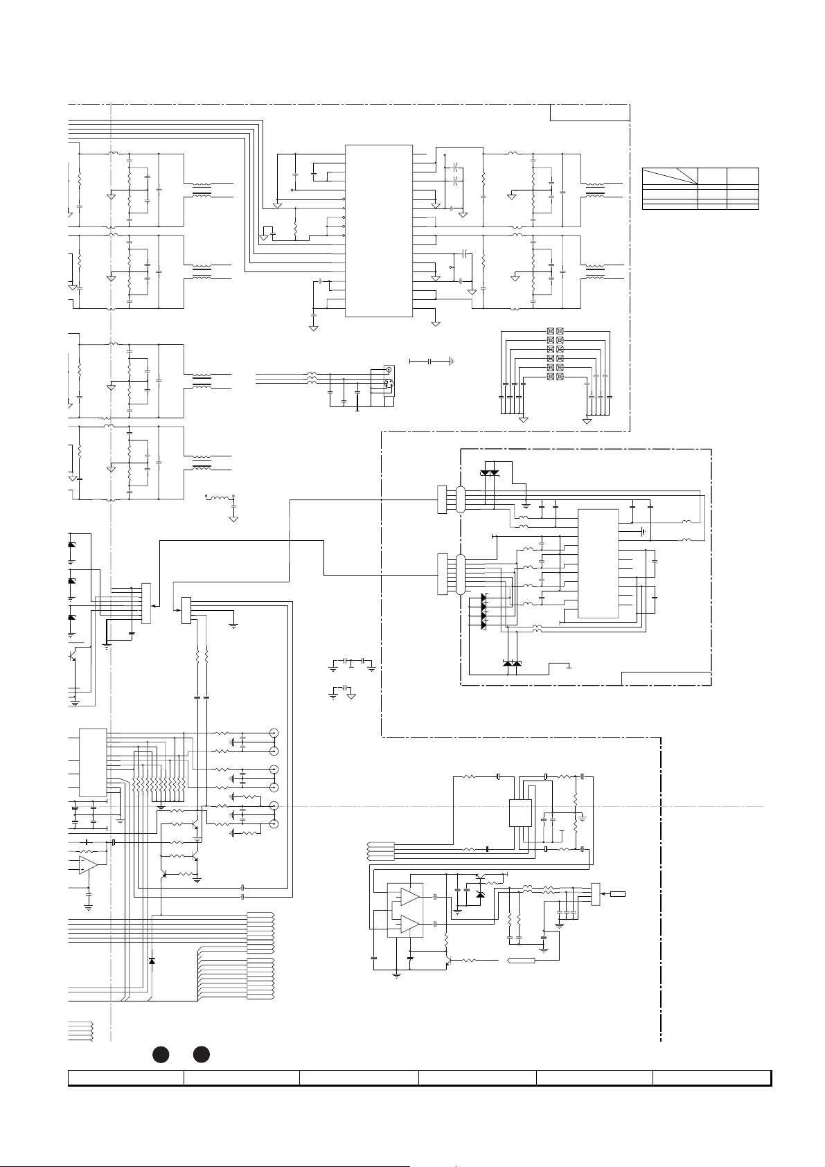
*R506
*C595
L504
*/R507
*C596
L505
L518
*R508
*C597
L519
L516
F
*R509
*C598
PRB
ZD102
7V
PBR
ZD104
7V
YG
ZD106
7V
CVBS1
Q108
C945
D
IC405
TC4052BFN
H MULTIPLEXER
X0
13
X1
X
X2
X3
Y0
3
Y1
Y
Y2
Y3
16
VDD
A
B
7
INH
VEE
GND
C453
C452
100UF
104
C455
C454
100UF
104
C440 47PF
R435 33K
2
1
3
IC404A
4
C444
104
L507
30uH
L517
30uH
+7V
-7V
L506
30uH
*R515
*R516
*R519
30uH
30uH
*R521
VIDEO_SW
CVBS1
12
14
15
11
1
5
2
4
10
9
6
8
C441
10UF
HT-CN400DVH/HT-CN400DVE/HT-CN500DVH/HT-CN500DVE
MAIN PWB-A1
L500 30uH
C505
104
R510
*R511
L501 30uH
L502 30uH
L503
30uH
102
C578
102
102
C584
C585
ZD128
7V
*R512
6.2 OHM
102
C579
102
C586
FB118
C506
104
C504
104
C508
104
R513
R514
6.2 OHM
C532
104
SUB+ SUB-
SL+
SR+
C+
L+
R+
102
C580
C184
FB117
15PF
601
601
FB105
601
FB106
601
FB107
601
FB108
601
FB109
601
FB110
601
ZD125
7V
15 OHM
*C571
+
*R505
C529
104
C594
471
ZD127
7V
1
2
3
4
5
VGND
1
2
3
4
5
6
7
8
ZD120
7V
ZD121
7V
ZD123
7V
ZD124
7V
ZD126
7V
C507
104
C509
104
C537
104
JK500
C185
15PF
C186
15PF
C187
15PF
C188
15PF
C189
15PF
VGND
L508
31
*C572
INDUCTOR 4
L511
31
C573
0.47UF
INDUCTOR 4
SL-
SR-
C-
L-
R-
102
C582
C581
102
C587
JK102
1
AOR
3
AOL
5
BGND
7
B
9
GGND
11
G
13
R GND
15
R
17
VGND
19
VOUT
21
SHIELD
SCART_21PIN
VGND
102
DATAGND
102
C583
102
C588
AGND
SWTCH
CLKOUT
BLNKGND
SL+
SL-
24
SUB+
SUB-
24
C589 102
C190
15PF
2
AIR
4
6
AIL
8
10
12
DATA
14
16
BLNK
18
20
VIN
VGND
Dimensions
Installation Point
R505 R506 R507 R508 R509
R515 R516 R517 R518 R519
R520 R521 R522 R511 R512
C595 C596 C597 C598 C571
C572 C574 C575 C576 C577
C191
15PF
FB119 601
FB120 601
C192
15PF
C193
15PF
MODEL
HT-CN500DVH/
HT-CN500DVE
15 OHM 22 OHM
4.7 OHM 6.2 OHM
470 PF 330 PF
0.68 UF 0.47 UF
HT-CN400DVH/
HT-CN400DVE
SCART PWB-A2
10UF
1K
R629 4.7 OHM
C625
104
12
3
4
LIN
VSS
8
+12V(IN)
L602 10uH
L603 10uH
R630 4.7 OHM
C626
104
EARDEC
C702
10UF
SDA
SCL5VDD6ROUTLOUT7RIN
C700
10uF
EARDEC
R619
C696
4.7K
IC608
PT2259
VOLUME
CONTROL
C697
4.7K
10UF
Q607
R628
C945
100UF
5.6V
C643
ZD605
C644
R626
4.7K
PH_MUTE
C698
R621
10UF
1K
100K
R623
C647
104
100K
+7V
C641
100UF
R624
C699
R622
1K
10UF
C703
10UF
R631
2.2 OHM
R632
EARDEC
2.2 OHM
C678 33PF
CN609
P_L_OUT
1
2
RB303
3
FROM
4
EARPHONE PWB
P22 2-B
33PF
C692
C689
33PF
C535
104
L509
31
C538 104
*C574
104
C539
C533
104
30uH
C536
104
*R517
C540
104
*C575
C541
104
*R518
C534
104
30uH
30uH
C556
104
C558
104
*C576
C559
104
*R520
C554
104
C557
104
C560
104
*C577
C561
104
*R522
C555
104
CN202
8
7
CN203
6
5
4
3
2
1
C224
10uF
R498 6.8K
R497 6.8K
S-B
S-A
CON5
R456 6.8K
R455 6.8K
R454 6.8K
R453 6.8K
R452 6.2K
R451 6.2K
R450 6.8K
R449 6.8K
R457 6.8K
R458 6.8K
R436
1K
R438
4.7K
R437
1K
R439
R440
Q401
A733
D401 1N4148
LMUTE
C+
24
C-
INDUCTOR4
L510
31
SR+
24
SR-
INDUCTOR4
L512
31
R+
24
R-
INDUCTOR4
L513
31
L+
2
L-
4
INDUCTOR4
VCC33E VCC33E
FB121
C623
104
1
2
3
4
5
1K
R135
R136 1K
10UF
10UF
C182
C183
R441 8.2K
R442
8.2K
R443 8.2K
R444 8.2K
R447 47K
R445 1K
4.7K
Q403
C2878
10K
RO
LO
R4461 1K
R448 47K
Q402
C2878
C41
C42
LINE-MUTE
PRE-L
PRE-R
PRE-SL
PRE-SR
PRE-C
PRE-SUB
AUX0
AUX1
MUTE
BASS
STO
DVD
EARDEC
IR
VFD-DA
VFDCLK
VFDCE
C446
C447
101
C448
101
C449
101
C450
101
C451
101
10UF
10UF
101
LINE-MUTE
PRE-L
PRE-R
PRE-SL
PRE-SR
PRE-C
PRE-SUB
AUX0
AUX1
EARDEC
VFD-DA
VFDCLK
CVBS1
YG
PBR
MUTE
VFDCE
C501
104
+3.3V
C500
104
JK401
6
9
5
4
8
3
2
7
1
RCA6
BASS
STO
DVD
IR
C502
104
R500
10K
FB111 601
FB112 601
FB113 601
19
20
GNDR1
21
VREG1
22
VREG1
23
VL
24
CONFIG
25
PWRDN
26
TRI-STATE
27
FAULT
28
TWARN
29
INLA
30
INLB
31
INRA
32
INRB
33
VREG2
C524
34
104
VREG2
35
VSIG
36
VSIG
C527
104
C194
C196
47PF
47PF
C195
47PF
VGND
C442
104
C431
VGND
C445
104
IC609
TP5228
DRIVER
W/MUTE
IC500
STA505
POWER AMP.
JK101
104
PRE-L
PRE-R
2259CL
2259DA
3
6
5
C642
100UF
4
PRE-L
PRE-R
2259CL
2259DA
OUTPL
OUTPL
PGND1P
PGND1N
OUTNL
OUTNL
OUTPR
OUTPR
PGND2P
PGND2N
OUTNR
OUTNR
VGND
-
+
+
-
VCC1P
VCC1N
VCC2P
VCC2N
+28V
18
NCGNDREF
GNDS
8
2
C562
1000UF
17
+
16
15
+
C565
14
1UF
13
12
C503
11
104
10
9
8
C566 1UF
7
6
+28V
5
4
3
2
1
C1021
102(
RB203
RB202
R620
100UF
C635
220UF
1
C636
220UF
7
R627
100K
Q606
C945
C701
4.7U
F
TCLOSE-SW
TOPEN-SW
LSW
TRAY-REV
• The numbers 13 to 14 are waveform numbers shown in page 37.
7
8 9 10 11 12
Figure 19 SCHEMATIC DIAGRAM (6/12)
– 19 –
Page 20
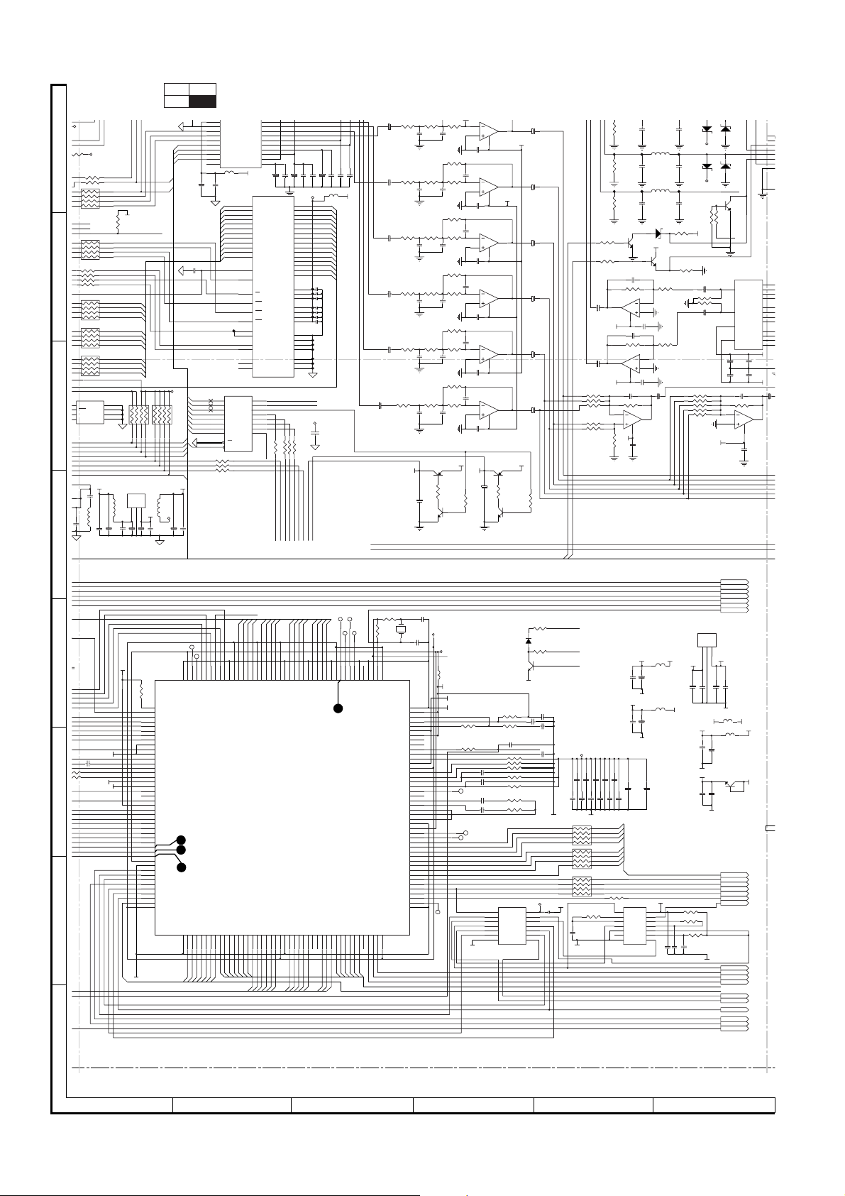
HT-CN400DVH/HT-CN400DVE/HT-CN500DVH/HT-CN500DVE
S
E
ZD103
ZD104
24
5
T
T
A
A
R
4
0
9
O
R
SITUATION :
R402
VCC33E
105
VC33
A
PEN
110 33 OHM AMCLK
111 33 OHM
RA101 33x4
18
27
36
45
RA102 33x4
45
36
27
18
60
61
62
63
B
RA104 10x4
45
36
27
18
RA105 10x4
45
36
27
18
RA106 10x4
45
36
27
18
VCC
WC
C
SCL
GND4SDA
IC107
TA24C02N
EEP ROM
K
C141
22PF
L101 10uH C142 102
C1006
D
33 OHM
33 OHM
33 OHM
33 OHM
S0
S1
S2
VC33
104
R174
4.4K
C1005
10UF
DB[0..15]
1
2
3
BICK
LRCK
SD0
SD1
SD2
VC33
VIDEO_SW
MA0
MA1
MA2
MA3
MA4
MA5
MA6
MA7
MA8
MA9
MA10
MA11
MA[0..11]
18
27
36
45
18
27
RA117
4.7Kx4
IC114
RT9164
FB102
100 OHM
+5V_1
123
C1001
104
C1003
C1002
C1004
10UF
10UF
104
6
7
8
9
DOUT
10
72CE
11
12
72CLK
13
72DA
14
FB115
104
C151 10UF
C152
C100
10PF
RCLK
CKE
CS0#
RAS0#
CAS#
WE#
DQMX
BANK0
BANK1
IC109
4MX16Y3VTW
DRAM
C199
+5V
104
74HC374
3
4
7
8
13
D1
14
D2
17D0D3
D4
1
LCS1#
11
R119 33 OHM
R120 33 OHM
R121 33 OHM
VCC
RA118
4.7Kx4
36
45
FB101
100 OHM
VCC
C1000
10UF
OUT2R
DVDD
DGND
OUT2L
DIN1
OUT1R
DIN2
VOUT1L
DIN3
DOUT
ML/I2S
VMID
MC/IWL
VREFP
MD/DM
VREFN
MUTE REFADC
601
VCC
MA0
23
MA1
24
MA2
25
MA3
26
MA4
29
MA5
30
MA6
31
MA7
32
MA8
33
MA9
34
MA10
22
MA11
35
38
37
18
17
16
15
39
20
21
36
40
IC108
D0 Q0
D1 Q1
D2 Q2
D3 Q3
D4 Q4
D5 Q5
D6 Q6
D718Q7
OE
CLK
23
22
21
20
AINL
19
AINR
18
17
16
15
A0
A1
A2
A3
A4
A5
A6
A7
A8A9DQ8
A10
A11
CLK
CKE
IC109
CS19VCC
RAS
CAS
WE
DQML
DQMH
BA0
BA1
NC
NC
2
5
6
9
12
15
16
19
SW1_VIDEO
C153 10UF
C154 104
DQ0
DQ1
DQ2
DQ3
DQ4
DQ5
DQ6
DQ7
DQ9
DQ10
DQ11
DQ12
DQ13
DQ14
DQ15
VCC
VCC
VCCQ
VCCQ
VCCQ
VCCQ
VSSQ
VSSQ
VSSQ
VSSQ
VSS
VSS
VSS
33 OHM
R122 33 OHM
R123 33 OHM
R124
SYR
RDS-DATA
TU-CE
TU-DI
C155 10UF
TUPO
TU-CL
33 OHM
R125
YU-DO
C160
C156 104
C157 10UF
C158
C159
FB116
VCC33
601
DB0
2
DB1
4
DB2
5
DB3
7
DB4
8
DB5
10
DB6
11
DB7
13
DB8
42
DB9
44
DB10
45
DB11
47
DB12
48
50
DB13
DB14
51
DB15
53
1
C144
14
C145
27
C146
3
C147
9
C148
43
C149
49
C144-C150(104)
C150
6
12
46
52
28
41
54
VCC
C143
104
SDB
TU5V
TU12V
104
104
104
10UF
L-A
104
C402
10UF
R-A
C161
VC33
C403
10UF
SL-A
C404
10UF
SR-A
C405
10UF
C-A
C406
SUB-A
10UF
TU-R
TU-L
R401 1K
R405 1K
R409 1K
R413 1K
R417 1K
R421 1K
4.7K
R403 1K
2
C408
C407
103
103
R408 22K
C413
151
R406 4.7K
R407 1K
C412
C411
103
103
R412 22K
C417
151
R410 4.7K
R411 1K
C416
C415
103
103
R416
C421
151
R414 4.7K
R415
C420
C419
103
103
R420 22K
C425
151
R418 4.7K
R419 1K
C424
C423
103
103
R424 5.6K
C429
332
R422 4.7K
R423 1K
C428
C427
103
103
Q104
A733
TU5V
R138
4.7K
C197
100UF
R137
10K
Q103
C945
1
3
4
IC401B
6
5
2
3
IC402B
6
5
IC403A
2
3
IC403B
6
5
8
IC402A
4
8
4
8
100UF
C198
Q105
C945
-12V
7
+12V
1
7
1
7
Q106
+12V+5V
A733
R140
4.7K
C410
104
C414
104
C418
104
22K
1K
C422
104
C426
104
C430
104
TU12V
7V
VCC33E
ZD1057VZD106
VCC33E
R167
10K
+12V(IN)
C456 10UF
R459 100K
R460 100K
C457 10UF
7V
7V
CVBS1
Q108
C945
R166 10K
DVD
IC405
TC4052BFN
4CH MULTIPLEXE
13
X
3
Y
16
VDD
7
VEE
C453
100UF
C455
100UF
C440 47PF
R435 33K
2
3
IC404A
4
-12V
C444
104
VID
CVB
12
X0
14
X1
15
X2
11
X3
1
Y0
5
Y1
2
Y2
4
Y3
10
A
9
B
6
INH
8
GND
+7V
C452
104
C454
104
-7V
C
1
1
C432
10UF
C433
10UF
C434
10UF
C435
10UF
C436
10UF
R425 47K
S-BLNK
S-SWTCH
R426 68K
R491 68K
R427 360K
R428 360K
C437
10UF
R139
10K
R128
C176
75 OHM
471
L104 2.4UH
YDAC YG
R129
C178
75 OHM
471
L105 2.4UH
VDAC
R130
C180
75 OHM
471
ZD109
4.7K
R131
Q101
C945
VCC
4.7K
R132
C458
47PF
R462 10K
IC406A
C459
10UF
C461
10UF
IC401~404/IC406
RC4558D
R429
56K
-12V
+12V
R430
1
4
C462 104
C460 47PF
R464 10K
IC406B
7
8
C463 104
C438 47PF
6
5
8
+12V
2
3
6
5
33K
7
IC404B
C443
104
C177
471
C179
471
CVBS
C181
471
7V
1K
R133
Q102
C945
R134
75 OHM
1K
R461
R463
1K
R431 47K
R432 68K
C439
R433 68K
10UF
R434 68K
R492 68K
TCLOSE-SW
TCLOSE-SW
TOPEN-SW
TOPEN-SW
LSW
LSW
TRAY-REV
TRAY-REV
TRAY-FWD
TRAY-FWD
DMUTE
DMUTE
14
13
12
11
10
9
8
FB903
FB904
601
601
D3V
C898
R8115 10K
R8113
C899
151
104
OSCIN
OSCIN
IC810
RT9164
123
D5V
A3V
C955 47UF
C952A 104
C953A 47UF
C954A 104
100 OHM
R8109
330 OHM
C81
221
AGND
D2V
HD[0..7
DCI_ERR
DCI_FDS
DCLK
HDACK#
DCI_REQ
LWRHL
LOE#
TDMFS
TDMCLK
TDMDR
HWAITB
HIRQB
LCS1#
FGO
RESB
GU
DGND
FB901
601
D3VA3V
A3VRF3V
601
FB902
C957 104
C956A 47UF
Q903A
C945
D3V
C959 104
C958 47UF
DGND
RB
FR
POWE
P25 1
HD[0..7]
DCI_ERR
DCI_FDS
DCLK
HDACK#
DCI_REQ
LWRHL
DGND
LOE#
TDMFS
TDMCLK
TDMDR
HWAITB
HIRQB
LCS1#
FGO
RESB
GU
D5V
DVD-CDB
LDON1
LDON2
DEFECTO
XHTR
T20
C895
E
103
849
71
850
71
C
F
C
D1
D0
T
L
L
C
DO
DO
O
O
G
..8]
SREF
R8116
6.8K
1
2
AD0
3
4
5
6
7
8
9
10
11
DGND
12
C851
104
100K
4.7K
D3V
13
14
15
16
17
18
AGND
19
20
21
22
23
24
25
26
27
28
29
30
31
32
33
34
35
36
FGO
37
INT_DEC
38
RDY
39
RESB
40
RD
41
42
43
44
WR
LCS1#
D8
DGND
AD1
AD0
JV
RREC
RF-PH
RF-BH
TE
FE
TEST0
EFMINP
TEST1
EFMINN
SLCLPFO
SLCLPFI
SLC01
SLC02
AVDD1
AVSS
BHC
WO
TEC
VREF
TSTD1
TSTD0
F0
BST
TBAL
FBAL
SGC
SLDO
SPDO
TDO
FDO
DVDD0
DVSS
FG
HIRQB
HWAITB
HRESB
HRDB
HWRB
HCSB
HDAT0
DVDD1
176
DVSS
7
8
6
DVSS45HDAT146HDAT2
174
175
HFLIO
DVDD0
47
D9
D10
WRQ_INT
R2IO0
R2IO6
R2IO7
T19
163
164
170
171
172
165
166
167
168
169
173
MD6
MD7
RFP1
RFP2
RFP3
RFP0
DVSS
TESIO
DVDD1
DEFECTI
DEFECTO
HDAT348HDAT449HDAT550HDAT651HDAT752HADR053HADR154HADR255HADR356HADR457HADR558HADR659MA062MA163MA264MA365MA468MA569MA670MA771MA872MA973MA1074HADR778HADR879HADR980HADR1081HADR1182HADR12
D11
D12
D13
D14
D15
A1A2A3A4A5A6A7
R2IO4
R2IO5
R2IO2
R2IO1
R2IO3
156
157
158
159
161
162
155
160
MD0
MD1
MD2
MD3
MD4
MD5
DVDD3
IC803
LC78663NRW
DVD FRONT END
MWEB60MRAS1B61DVDD366DVSS
R2A2
R2A0
R2A1
R2A3
MWEB
MRAS1B
DVDD3
R2IO15
R2IO14
152
153
154
DVSS
MD1 4
MD15
67
R2A4
R2A5
R2IO12
R2IO11
R2IO9
R2IO8
R2IO13
R2IO10
146
147
148
150
151
144
145
149
MD 9
MD 8
DVSS
MD1 0
MD1 1
MD1 2
MD1 3
MOEB75MCASUB76MCASLB77C2F84ROMXA85ROMCK86LRSY87DVDD1
R2A8
R2A6
R2A7
MOEB
MCASUB
MCASLB
DVSS
T15
143
DVDD1
9
A8A9A10
T13
T14
T12
139
140
141
142
FSX
EFLG
DOUT
DVDCKIO
A11
A12
137
138
TEST2
83
A13
R891 330OHM
134
135
136
DVSS
XOUT
X16MIO
C865
10PF
XL801
R890
16.9344MHz
VCOCTL
EFMOUT
AVERRB
AVSCTB
AVDACK
AVACKO
AVREQI
DVDD0
VRPFR
VPDO
AVDD3
JVRVO
JVAIN
JVCPC
AVDD2
DVDFR
DVDD0
EMPH
D3V
10PF
C866
D2V
L802
601
A2.5V
AGND
132
DVSS
VCOC
AVSS
JVAO
JVCPI
AVSS
CDFR
FISET
PISET
PCN
LF3
LF2
LF1
FPDO
PPDO
DVSS
PCK
AVD7
AVD6
AVD5
AVD4
AVD3
AVD2
AVD1
AVD0
DVSS
DGND
131
130
129
R887 10K
128
127
126
125
124
R883 6.8K
123
122
121
120
119
118
117
116
115
114
113
112
111
110
109
108
107
106
105
104
103
102
101
100
99
98
97
96
95
94
93
92
91
90
89
C859 104
C858
T11
C856 104
C855 104
T10
T9
AVERRB#
AVSCTB
AVDACK#
AVDENB#
AVREQI
INT_DEC
T8
RD
IC807
SN74LVC32ANS
QUAD 2-1/P OR GATE
1M
133
XIN
DVDD2
88
R889 5.6K
R888
220 OHM
104
AVD7
AVD6
AVD5
AVD4
AVD3
AVD2
AVD1
AVD0
1
2
3
4
5
6
D901
1N4148
561
C861
R882 10K
R881 1.2K
R880 1.8K
R879 22K
R878 22K
R876 1.2K
680 OHM
R875
A1
VCC
B4
B1
A4
Y1
Y4
A2
B3
B2
Y2
A3
VSS7Y3
R894 68K
R893
Q904A
C945
AGND
C854 104
C863 104
C862 104
ADJV
C860 103
D3V
14
13
12
11
10
9
8
ADTE
10K
DEFECTO
TE_BIAS
D3V
C875 104
C874 104
RA801 10x4
18
27
36
45
18
27
36
45
RA802 10x4
RA803 10x4
18
27
36
45
C896
DGND
104
R8106
C897
151
DGNDDGND
LCS1#
RDY
C877 104
C876 104
DGNDAGND
C881 104
C879 104
C880 104
C878 104
R873 10 OHM
100 OHM
C883 104
C882 104
C884 104
HD7
HD6
HD5
HD4
HD3
HD2
HD1
HD0
1
2
3
4
5
6
SN74HC14NS
INVERTER
C961 104
RF5V
C951A 104
C885 47UF
I1
O1
I2
O2
I3
O3
VSS7O4
IC808
MGND
AGND
VCC
D5V S5V
C960 47UF
C950A 47UF
C887 47UF
I6
O6
I5
O5
I4
H
• NOTES ON SCHEMATIC DIAGRAM can be found on page 11.
1
23456
Figure 20 SCHEMATIC DIAGRAM (7/12)
– 20 –
Page 21
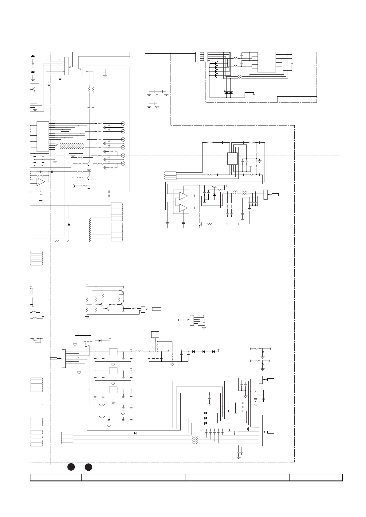
HT-CN400DVH/HT-CN400DVE/HT-CN500DVH/HT-CN500DVE
ZD104
4
R GND
33PF
CN609
1
2
3
4
DATAGND
BLNK
BLNKGND
VIN
EARPHONE PWB
P22 2-B
RB303
FROM
14
16
18
C193
15PF
20
VGND
SCART PWB-A2
7V
YG
ZD106
7V
CVBS1
Q108
C945
VD
IC405
TC4052BFN
CH MULTIPLEXER
13
X
3
Y
16
VDD
7
INH
VEE
GND
C453
C452
100UF
104
C455
C454
100UF
104
C440 47PF
R435 33K
2
1
3
IC404A
4
C444
104
CN202
VIDEO_SW
8
CVBS1
7
CN203
6
5
4
3
2
1
C224
10uF
12
X0
14
X1
15
X2
11
X3
1
Y0
5
Y1
2
Y2
4
Y3
10
A
9
B
6
8
R458 6.8K
R498 6.8K
R497 6.8K
+7V
S-B
S-A
-7V
C441
10UF
1
2
3
4
5
CON5
1K
R135
R136 1K
10UF
10UF
C182
C183
R447 47K
R448 47K
10UF
C446
101
C447
101
C448
101
C449
101
C450
101
C451
101
10UF
LINE-MUTE
PRE-L
PRE-R
PRE-SL
PRE-SR
PRE-C
PRE-SUB
AUX0
AUX1
MUTE
BASS
DVD
EARDEC
VFD-DA
VFDCLK
VFDCE
JK401
6
9
5
4
8
3
2
7
1
RCA6
STO
IR
R441 8.2K
R442
8.2K
R443 8.2K
R444 8.2K
R456 6.8K
R455 6.8K
R454 6.8K
R453 6.8K
R452 6.2K
R451 6.2K
R450 6.8K
R449 6.8K
R457 6.8K
R436
R438
R437
R439
R440
Q401
A733
D401 1N4148
LMUTE
R445 1K
4.7K
1K
Q403
C2878
4.7K
1K
10K
RO
LO
R4461 1K
Q402
C2878
C41
C42
LINE-MUTE
PRE-L
PRE-R
PRE-SL
PRE-SR
PRE-C
PRE-SUB
AUX0
AUX1
MUTE
BASS
STO
DVD
EARDEC
IR
VFD-DA
VFDCLK
VFDCE
C442
104
VGND
C445
104
IC609
TP5228
DRIVER
W/MUTE
104
C431
PRE-L
PRE-L
PRE-R
PRE-R
2259CL
2259CL
2259DA
2259DA
8
3
-
+
6
+
5
-
2
4
C642
100UF
C701
4.7U
5
6
7
8
ZD120
7V
ZD121
7V
ZD123
7V
ZD124
7V
ZD126
7V
R619
10UF
C696
4.7K
IC608
PT2259
VOLUME
CONTROL
C697
R620
4.7K
10UF
Q607
R628
1K
C945
100UF
100UF
C635
220UF
1
C636
220UF
7
R627
100K
F
5.6V
C643
ZD605
C644
C625
Q606
C945
104
R626
4.7K
PH_MUTE
FB107
601
FB108
601
FB109
FB110
ZD125
7V
12
3
LIN
8
+12V(IN)
L602 10uH
L603 10uH
R629 4.7 OHM
R630 4.7 OHM
C626
104
EARDEC
C188
15
15PF
R
17
VGND
C189
19
15PF
VOUT
21
SHIELD
SCART_21PIN
VGND
601
601
VGND
R632
EARDEC
C698
R621
10UF
1K
100K
R623
C647
104
100K
+7V
C641
100UF
R624
C699
R622
1K
10UF
C703
10UF
R631
2.2 OHM
P_L_OUT
2.2 OHM
EARDEC
C692
C678 33PF
C689
33PF
C702
10UF
4
VSS
SDA
SCL5VDD6ROUTLOUT7RIN
C700
10uF
TCLOSE-SW
TOPEN-SW
LSW
TRAY-REV
TRAY-FWD
DMUTE
OSCIN
IC810
RT9164
5V
C952A 104
DGND
901
902
Q903A
C945
HD[0..7]
DCI_ERR
DCI_FDS
DCLK
HDACK#
DCI_REQ
LWRHL
LOE#
TDMFS
TDMCLK
TDMDR
HWAITB
HIRQB
LCS1#
FGO
RESB
GU
+12V(IN)
R613
100K
R611
9.1K
SN601
10K(PTC)
Q601
A733
R610
R612
15K
601
D3V
A3V
601
D3V
CN602
6.8V
1
2
+12V(IN)
3
4
RB904
FROM
POWER PWB
P25 12-D
5
6
7
8
MUTE
LINE-MUTE
IR
VFD-DA
VFDCLK
VFDCE
-24V
AC1
AC2
MUTE
LINE-MUTE
IR
VFD-DA
VFDCLK
VFDCE
15K
D604
1N4001
33PF
33PF
33PF
C164
C163
C162
C616
C627
104
220UF
C628
C617
220UF
104
C618
C629
104
220UF
R607
10 OHM
560OHM 1W
R608
ZD602
11.9-12.4V
R615
2.2K
Q602
C945
+5V_1
123
IC603
123
IC604
1
IC602
2
R616
100K
C630
220UF
IC603,604
BA05T
C631
220UF
3
C632
220UF
C637
100UF
C638
100UF
Q603
C945
Q604
A733
C612
104
R617
47 OHM 2W
+5V
C619
104
S5V
C620
104
S8V
REGULATOR
C621
104
+12V
C645
104
-12V
C646
104
D609 1N4148
CN601
2
P24 2-G
1
FROM
FAN MOTOR
IC605
B1117N
VOLTAGE REGULATOR
123
FB600
100 OHM
C659
104
C660
10UF
IC602
L7808
120 OHM
C661
10UF
R637
+2.5V +3.3V
C662
104
PH_MUTE
R638
150 OHM
RB905
FROM
POWER PWB
P25 12-B
CN606
+28V
1
2
3
C615
104
4
R494
150 OHM
D601
1N4148
C622
C633
104
10UF
SPK_MUTE
R633
R634
R635
R636
1N4148
D610 1N4148
D607 1N4148
D608 1N4148
C677
33 OHM
33 OHM
33 OHM
33 OHM
1N4148
C648
100UF/50V
C650
C651
C649
ST_MUTE
33PF
C694
33PF
C688 33PF
C690 33PF
C691 33PF
B5V
D603
D602
+12V
-12V
C656 33PF
C655 33PF
33PF
33PF
C664
33PF
C658
33PF
33PF
C693
33PF
AUX0
+5V
AUX1
33PF
C665
33PF
C666
R495
150 OHM
100UF
1
2
3
4
5
6
7
8
9
10
11
12
13
14
+7V
ZD401
5.6V
-7V
ZD402
5.6V
CN608
3
RB906
2
1
FROM
POWER PWB
P25 12-E
B5V
C640
C624
104
CN600
RB304
FROM
DISPLAY PWB
P22 3-C
• The numbers 6 to 9 are waveform numbers shown in page 36.
7
8 9 10 11 12
Figure 21 SCHEMATIC DIAGRAM (8/12)
– 21 –
Page 22
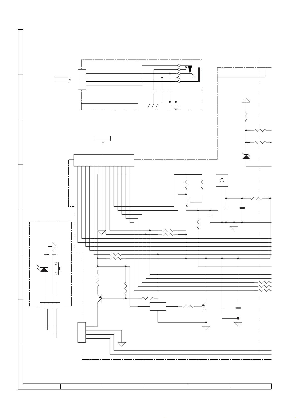
HT-CN400DVH/HT-CN400DVE/HT-CN500DVH/HT-CN500DVE
A
RB303
1
CN609
TO
MAIN PWB
P19 11-6
B
2
3
4
C301 104
C302 104
JK301
DISPLAY PWB-B1
104
C303
EARPHONE PWB-B2
R301
22K
R302
R308
C306
100UF
1K
R303
1K
ZD301
6V
100
C
CN600
RB304
12345678910111213
AC1
AC2
-24V
LED3
POW
B5V
D
VFD_SDA
STAND-BY
E
PWB-B3
TO
MAIN PWB
P21 11-H
VFD_SCL
+5VIRVFD_DATA
VFD_CLK
14
VFD_STB
R313 4.7K
R314 4.7K
R306
100K
Q301
C945
R307
100K
R320
560
SN201
SENSOR
123
C309
221
C304
104
R304 1K
R312 33
F
LD301
RB301
4321
G
TA301
ON/STAND-BY
CN301
R321
1K
4
3
2
1
R322
10K
Q303
CM5051
IMP809SEUR
H
• NOTES ON SCHEMATIC DIAGRAM can be found on page 11.
1
23456
Figure 22 SCHEMATIC DIAGRAM (9/12)
R315 10K
IC302
RESET
– 22 –
R311 1
R309 1
R310 1
R305
23
1K
1
Q302
CM5051
C305
104
C307
100UF
Page 23
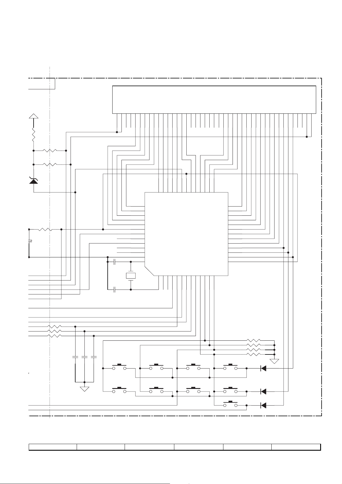
PWB-B1
HT-CN400DVH/HT-CN400DVE/HT-CN500DVH/HT-CN500DVE
DP301
FL DISPLAY
R301
22K
R308
C306
100UF
R302
1K
R303
1K
ZD301
6V
100
123456789
40
41
42
43
44
45
46
47
LD4
48
LD3
49
LD2
50
LD1
51
52 14
C310
150P
C311
150P
XL301
455KHz
10111213141516171819202122
33
34
35
36
37
38
39
GR8
GR7
GR6
GR5
GR4
GR3
GR2
GR1
VDD
PCON
LED4
LED3
LED2
LED1
GND
OSC1
OSC2
SW2
123456789
SG20/GR9
SG19/GR10
VDTR6311A
FL DRIVER
SW3
R/C
DATA
VEE
VDD
IC301
SCL
SDA
29
30
31
32
SG16
SG11/KS11
SG17/GR12
SG18/GR11
SG10/KS10
CLK
STBK1K2K3K4
101112
24252627282930313233343536373839404142
23
27
28
SG13
SG14
SG15
SG9/KS9
SG8/KS8
SG7/KS7
SG6/KS6
SG5/KS5
SG4/KS4
SG3/KS3
SG2/KS2
SG1/KS1
13
SG12
VDD
26
25
24
23
22
21
20
19
18
17
16
15
43
R311 100
R309 100
R310 100
307
00UF
R316 10K
R317 10K
R318 10K
TA302
STOP
C313 15P
C312 15P
7
C314 15P
TA303
FAST FORWARD
8 9 10 11 12
TA304
FAST REVERSE
TA305
VOLUME DOWN
TA306
MODE
TA307
FUNCTION
VOLUME UP
OPEN/CLOSE
TA308
TA309
PLAY
TA310
R319 10K
D301
D302
D303
1N4148
1N4148
1N4148
Figure 23 SCHEMATIC DIAGRAM (10/12)
– 23 –
Page 24

HT-CN400DVH/HT-CN400DVE/HT-CN500DVH/HT-CN500DVE
A
B
C954B
C
C955B
C956B
TOP249Y
POWER SWITCH
D901B BYV26D
IC903
D
E
AC POWER SUPPLY CORD
230 V, 50/60Hz
FAN MOTOR (225)
F
RD
BK
1
2
CN601
TO
MAIN PWB
P21 9-F
G
H
• NOTES ON SCHEMATIC DIAGRAM can be found on page 11.
1
23456
Figure 24 SCHEMATIC DIAGRAM (11/12)
IC905
NCP1050DIP
SWITCH REGULATOR
– 24 –
Page 25

HT-CN400DVH/HT-CN400DVE/HT-CN500DVH/HT-CN500DVE
1
C950B
C952B
2
3
CN606
TO
MAIN PWB
4
P21 10-F
IC904
TL431
VOLTAGE
REGULATOR
CN602
TO
MAIN PWB
P21 7-F
22
CN608
TO
MAIN PWB
P21 11-G
POWER PWB-C
7
8 9 10 11 12
Figure 25 SCHEMATIC DIAGRAM (12/12)
– 25 –
Page 26

HT-CN400DVH/HT-CN400DVE/HT-CN500DVH/HT-CN500DVE
1
0
6
4
FROM
FAN MOTOR
P31 8-D
114 12
13
POWER PWB
P31 10-H
FROM
RB903
FROM
POWER PWB
P31 9-H
RB904
FROM
POWER PWB
P31 8-H
RB906
A
B
C
D
E
JK500
SPEAKER
TERMINL
SUBWOOFER
SURROUND
SPEAKER L-CH
SURROUND
SPEAKER R-CH
CENTER
SPEAKER
FRONT
SPEAKER L-CH
FRONT
SPEAKER R-CH
SPEAKER
TERMINL
JK101
VIDEO OUT
JK104
AUDIO OUT
AUDIO
INPUT2
AUDIO
INPUT1
JK500
12
4321
32
1
87654
–
1
–
–
18
–
–
1
–
10
15
18
1
10
15
18
12345 12345 678
8
1
5
10
15
9
16
36
35
5
30
10
25
15
20
19
21
3
36
35
5
30
25
20
19
64
49
48
33
36
35
5
30
1
50 55
60
45
5
40
10
35
2025
30
16
32
17
1 2 3
1 2 3
1 2 3
3 2 1
25
20
19
1
5
28
5
4
8
1
5
1
4
8
123
13579
111315
2468
1012141
1
64
51
60
55
50
4045
49
48
1
510
35
40
54
5
50
10
45
15
40
20
35
30
25
28
14
10
2025
15
5
4
8
F
AM LOOP
ANTENNA
JK001
FM ANTENNA
G
2
1
1 2 3 4 5
6 7 8
MAIN PWB-A1 (TOP VIEW)
H
• The numbers 1 to 14 are waveform numbers shown in page 36, 37.
1
23456
Figure 26 WIRING SIDE OF P.W.BOARD (1/6)
– 26 –
5
4
1
8
1
20
11
15
5
10
1
24
510
20
15
12
13
RB203
15
SCART
4
1
13
2
5
8
Page 27

HT-CN400DVH/HT-CN400DVE/HT-CN500DVH/HT-CN500DVE
13
48
33
4
1
FROM
POWER PWB
P31 10-H
RB903
4321
3
21
64
49
1
50 55
60
45
5
40
10
35
2025
30
16
32
17
5
8
FROM
FROM
POWER PWB
P31 9-H
12 9
RB904
32
1
5
8
87654
1 2 3
1 2 3
1 2 3
3 2 1
1
28
1
4
4
1
POWER PWB
P31 8-H
RB906
123
13579
2468
1
64
60
55
50
49
48
1
510 15
40
54
50
45
40
35
30
14
5
10
2025
15
4
5
8
4
1
1113151719 2123 25
1012141618 2022 24
51015
354045
3035
1
5
10
15
20
25
2728
5
8
5
8
FROM DVD
MECHANISM UNIT
with PICKUP
PWB (210)
26
16
17
20
25
30
32
33
20
25
1
176
510152025303540
175
170
165
160
155
150
145
140
21
135
134
133
105
104
110 115 120 125 130 135 140 145 150 155
100
95
90
85
80
75
70
65
60
55
50
53
52
1
5
15
20
FROM DVD
MECHANISM UNIT
with SPIN/SLED
7
9
101518
37
1
5
35
36
202530
38
28
27
19
8
7
10
1
14
44
45
50
55
60
65
70
75
80
85
9095100105110115120125130
88
89
5
4
1
8
8
7
5510
1
14
MOTOR PWB (210)
123
20
15
11
8
246
135
5
4
3
2
1
1
5
10
1
45
FROM DVD
MECHANISM UNIT
with LOADING
MOTOR PWB (210)
8
6
156
157
160
165
170
175
180
185
190
195
200
205
51015202530354045
208
1
21
40
25
30 35
51015
1
20
11
2
3
1
8
5
1015
9
10
11
5
15
20
1
8
11
4
5
58
1
4
16
10
1
14
13
12
11
10
9
8
7
6
5
4
3
2
1
4
5
RB304
FROM
DISPLAY PWB
P30 4-C
10
1
2
3
4
RB303
FROM
EARPHONE PWB
P30 4-F
1
20
24
510
20
15
12
13
1
RB203
15
1 3 5 7 9 11 13 15 17 19 21
SCART
2 4 6 8 101214161820
7
8 9 10 11 12
SCART PWB-A2
8
8
7
6
5
4
3
2
1
1
Figure 27 WIRING SIDE OF P.W.BOARD (2/6)
– 27 –
Page 28

HT-CN400DVH/HT-CN400DVE/HT-CN500DVH/HT-CN500DVE
MAIN PWB-A1 (BOTTOM VIEW)
A
B
C
3
2
D
1
E
15
10
F
5
1
G
SCART PWB-A2 (BOTTOM VIEW)
H
1
23456
Figure 28 WIRING SIDE OF P.W.BOARD (3/6)
– 28 –
Page 29

W)
HT-CN400DVH/HT-CN400DVE/HT-CN500DVH/HT-CN500DVE
3
2
1
15
1
16
20
10
25
5
30
OM VIEW)
7
8 9 10 11 12
Figure 29 WIRING SIDE OF P.W.BOARD (4/6)
– 29 –
Page 30

HT-CN400DVH/HT-CN400DVE/HT-CN500DVH/HT-CN500DVE
TA303
FAST
FORWARD
TA304
FAST
REVERES
TA305
VOLUME
DOWN
TA308
VOLUME UP
A
TA302
STOP
B
TA309
PLAY
C
TA306
MODE
TA307
FUNCTION
1
2
3
1
14
1
2
3
4
5
6
7
CN600
8
TO
9
MAIN PWB
P27 12-E
10
11
12
13
14
D
40
39
35
45
52
30
27
25
26
E
50
5
20
15
14
1
10
13
C301
C302
3
F
G
DISPLAY PWB-B1
2
1
TA310
OPEN/CLOSE
1
4
4
1
TA301
ON-STAND-BY
1
HEADPHONES
EARPHONE PWB-B2
JK301
RB303
4
4
3
CN609
2
TO
1
MAIN PWB
P27 12-F
H
STANDBY PWB-B3
1
23456
Figure 30 WIRING SIDE OF P.W.BOARD (5/6)
– 30 –
Page 31

HT-CN400DVH/HT-CN400DVE/HT-CN500DVH/HT-CN500DVE
POWER PWB-C
1
8
2
7
3
6
5
4 3
21
AC POWER
SUPPLY CORD
AC 230V,
50/60 Hz
FAN MOTOR (225)
RD
BK
CN601
TO
MAIN PWB
P26 3-A
1
2
1
2
1 2
2
3
4
5
6
1
34
COLOR TABLE
BR
BROWN
RD(R)
WH(W)
OR
YL
GR
BL
VL
GY
BK
PK
RED
ORANGE
YELLOW
GREEN
BLUE
VIOLET
GRAY
WHITE
BLACK
PINK
3
8
1
4
1
1
123
1
2345678
WH
RD
RD
WH
1234
CN608
TO
MAIN PWB
P27 9-A
7
8 9 10 11 12
CN602
TO
MAIN PWB
P26 5-A
CN606
TO
MAIN PWB
P26 4-A
Figure 31 WIRING SIDE OF P.W.BOARD (6/6)
– 31 –
Page 32

HT-CN400DVH/HT-CN400DVE/HT-CN500DVH/HT-CN500DVE
VOLTAGE
IC810 (RT9164)
PINS NUMBER 1 2 3
VOLTAGE
(DVD P LAY)
IC103 (74LS374)
PINS NUMBER
VOLTAGE
(DVD P LAY)
IC102 (74LS374)
PINS NUMBER
VOLTAGE
(DVD P LAY)
IC108 (74LS374)
PINS NUMBER
VOLTAGE
(DVD P LAY)
IC809 (LM358)
PINS NUMBER
VOLTAGE
(DVD P LAY)
5V 0V 3.3V
10 20
0V 5V
10 20
0V 5V
10 20
0V
12345678
1.1V 2.3V 0V 0V 1.6V 1.6V 1.6V 7.9V
5V
IC107 (24C02)
PINS NUMBER
VOLTAGE
(DVD P LAY)
IC801 (LA6560)
PINS NUMBER
VOLTAGE
(DVD P LAY)
PINS NUMBER
VOLTAGE
(DVD P LAY)
PINS NUMBER
VOLTAGE
(DVD P LAY)
PINS NUMBER
VOLTAGE
(DVD P LAY)
PINS NUMBER
VOLTAGE
(DVD P LAY)
IC104 (74LS157)
PINS NUMBER
VOLTAGE
(DVD P LAY)
12345678
0V 0V
12345678
0V 0V
910111213141516
3.6V 4.6V 2.5V 3.6V 3.6V 7.9V 1.1V
17 18 19 20 21 22 23 24
1.6V 1.6V 1.6V 1.6V 1.6V 1.6V 1.6V1.8V
25 26 27 28 29 30 31 32
1.6V 0.9V 0V 1.6V 5V 1.6V 1.6V 1.6V
33 34 35 36 37 38
1.6V 3.3V 2.5V 0V 0V 0V
56
0V 5V
0V 0V
7.9V 1.3V 1.3V 1.6V 3.6V 3.5V
4.2V 4.2V
0V 5V
0V
IC807 (74HC32)
PINS NUMBER
VOLTAGE
(DVD P LAY)
IC808 (874HC14)
PINS NUMBER
VOLTAGE
(DVD P LAY)
714
0V 3.2V
714
0V 3.2V
– 32 –
Page 33

IC608 (PT2259)
PINS NUMBER
VOLTAGE
(DVD P LAY)
IC609 (TP5228)
PINS NUMBER
VOLTAGE
(DVD P LAY)
IC115/IC 605 (B1117)
PINS NUMBER
VOLTAGE
(DVD P LAY)
IC114 (RT9164)
PINS NUMBER
VOLTAGE
(DVD P LAY)
IC603/IC604 (BA05T)
PINS NUMBER
VOLTAGE
(DVD P LAY)
IC602 (7808)
PINS NUMBER
VOLTAGE
(DVD P LAY)
IC003 (LC72720)
PINS NUMBER
VOLTAGE
(DVD P LAY)
PINS NUMBER
VOLTAGE
(DVD P LAY)
PINS NUMBER
VOLTAGE
(DVD P LAY)
IC002 (LC72131)
PINS NUMBER
VOLTAGE
(DVD P LAY)
PINS NUMBER
VOLTAGE
(DVD P LAY)
PINS NUMBER
VOLTAGE
(DVD P LAY)
IC110 (WM8772)
PINS NUMBER
VOLTAGE
(DVD P LAY)
PINS NUMBER
VOLTAGE
(DVD P LAY)
PINS NUMBER
VOLTAGE
(DVD P LAY)
PINS NUMBER
VOLTAGE
(DVD P LAY)
HT-CN400DVH/HT-CN400DVE/HT-CN500DVH/HT-CN500DVE
12345678
2.7V 2.8V 0V
12345678
2.3V 4.9V 2.3V 2.3V 2.3V 2.3V 4.9V
12 3
1.5V 2.8V 5.0V
12 3
5.7V 0V
12 3
6.5V 5V
12 3
11.5V 7.9V
12345678
2.4V 2.4V 4.8V 0V 2.4V 2.4V 0V 0V
910111213141516
0.4V 1.0V 1.5V 2.5V 2.5V 4.9V
17 18 19 20 21 22 23 24
4.4V 3.3V 3.0V 5V 5V 0V 0V 0V
12345678
2.4V 0V
910111213141516
0V 0V 0V 0V
17 18 19 20
1.0V 3.3V
12345678
910111213141516
0.9V 2.4V 4.2V 4.2V 0.1V 0V 5V 0V
17 18 19 20 21 22 23 24
2.5V 2.4V 2.5V 2.5V 2.5V 2.5V 2.5V 2.5V
25 26 27 28
2.5V 5V 0V 2.5V
0V
0V
1.4V0V 1.6V 1.6V 5V 0V 0.9V 0.8V
3.3V
0V 0V 0V5V 5V 4.6V
0V
5V 2.7V 2.8V 5.8V 5V
0V
0V 0V
4.8V 2.3V 4.8V 1.0V
2.4V
– 33 –
Page 34

HT-CN400DVH/HT-CN400DVE/HT-CN500DVH/HT-CN500DVE
IC802 (LA9703W)
PINS NUMBER
VOLTAGE
(DVD P LAY)
PINS NUMBER
VOLTAGE
(DVD P LAY)
PINS NUMBER
VOLTAGE
(DVD P LAY)
PINS NUMBER
VOLTAGE
(DVD P LAY)
PINS NUMBER
VOLTAGE
(DVD P LAY)
PINS NUMBER
VOLTAGE
(DVD P LAY)
PINS NUMBER
VOLTAGE
(DVD P LAY)
PINS NUMBER
VOLTAGE
(DVD P LAY)
12345678
2.6V 5V 3.6V 3.7V 3.7V 3.7V 3.7V 2.5V
910111213141516
2.5V 2.5V 2.5V 2.5V 2.5V 2.5V 5V 0.2V
17 18 19 20 21 22 23 24
3.8V 0.2V 0V 0V 0V 3.2V 0V 0V
25 26 27 28 29 30 31 32
0V 2.5V 2.5V 3.3V 5V 0V 3.2V 1.0V
33 34 35 36 37 38 39 40
2.0V 1.6V 1.6V 1.6V 1.6V 2.2V 1.7V 1.6V
41 42 43 44 45 46 47 48
1.7V 1.6V 0V 1.6V 1.2V 1.2V 2.4V 3.3V
49 50 51 52 53 54 55 56
1.2V 2.7V 1.6V 2.6V 2.4V 2.6V 2.6V 0V
57 58 59 60 61 62 63 64
0.6V 2.5V 2.5V 2.5V 2.5V 2.8V 5V 2.7V
IC503 DDX- 8000
PINS NUMBER
VOLTAGE
(DVD P LAY)
PINS NUMBER
VOLTAGE
(DVD P LAY)
PINS NUMBER
VOLTAGE
(DVD P LAY)
PINS NUMBER
VOLTAGE
(DVD P LAY)
PINS NUMBER
VOLTAGE
(DVD P LAY)
PINS NUMBER
VOLTAGE
(DVD P LAY)
PINS NUMBER
VOLTAGE
(DVD P LAY)
PINS NUMBER
VOLTAGE
(DVD P LAY)
IC001 (LA1837)
PINS NUMBER
VOLTAGE
(DVD P LAY)
PINS NUMBER
VOLTAGE
(DVD P LAY)
PINS NUMBER
VOLTAGE
(DVD P LAY)
PINS NUMBER
VOLTAGE
(DVD P LAY)
12345678
0V 0V 0V 0V 0V 0V3V 2.8V
910111213141516
1.3V 1.0V 1.6V 3.0V 0V 0V2.8V 3.2V
17 18 19 20 21 22 23 24
0V 0V 0V
25 26 27 28 29 30 31 32
1.4V 2.8V 0V 0V 0V 0V 0V3.0V
33 34 35 36 37 38 39 40
0.2V 0.2V 2.2V 3.0V 0V
41 42 43 44 45 46 47 48
0.2V 0.2V 0V 0V 0V 0V3.0V 2.8V
49 50 51 52 53 54 55 56
0V
57 58 59 60 61 62 63 64
0V
12345678
3.5V 8.6V 3.5V 3.5V 0.1V 0V 0.2V 8.6V
910111213141516
8.6V 1.3V 3.2V 0V 0V 7.5V 7.5V 4.3V
17 18 19 20 21 22 23 24
4.3V
25 26 27 28 29 30
0V
4.3V 4.3V 1.2V 2.8V
2.8V
0V 2.8V3.0V 0.2V
4.3V 4.3V 3.2V 3.2V 2.8V 3.4V 0.2V
3.6V 3.6V 3.6V 3.6V 1.8V
1.0V 0V 3.0V
0.2V 0.2V
0V 0.2V0V0.3V 3.0V 2.8V 1.4V
3.0V
– 34 –
Page 35

IC500/IC501/IC502 (STA505)
PINS NUMBER
VOLTAGE
(DVD P LAY)
PINS NUMBER
VOLTAGE
(DVD P LAY)
PINS NUMBER
VOLTAGE
(DVD P LAY)
PINS NUMBER
VOLTAGE
(DVD P LAY)
PINS NUMBER
VOLTAGE
(DVD P LAY)
HT-CN400DVH/HT-CN400DVE/HT-CN500DVH/HT-CN500DVE
12345678
0V 0V2.1V 2.1V 31.3V 0V 31.3V 2.1V
910111213141516
2.1V 2.1V 2.1V 2.1V0V31.3V 31.3V 0.4V
17 18 19 20 21 22 23 24
0V 0V 5.0V 5.0V 5.0V 0V 3.0V 3.0V
25 26 27 28 29 30 31 32
3.0V 3.0V 3.0V 0.2V 0.2V 0.2V 0.2V 0.2V
33 34 35 36
26.2V 26.2V 31.3V 31.3V
– 35 –
Page 36

HT-CN400DVH/HT-CN400DVE/HT-CN500DVH/HT-CN500DVE
WAVEFORMS OF DVD CIRCUIT
IC106 40PIN
1
IC106 PIN
IC106 PIN
IC106 6PIN
IC106 PIN
IC803 142PIN
9
IC803 33PIN
6
IC803 3PIN
IC803 33PIN
6
IC803 3PIN
IC106 39PIN
10
IC106 102PIN
11
– 36 –
Page 37

IC802 55PIN
12
HT-CN400DVH/HT-CN400DVE/HT-CN500DVH/HT-CN500DVE
IC503 50PIN
13
IC501 16PIN
14
– 37 –
Page 38

HT-CN400DVH/HT-CN400DVE/HT-CN500DVH/HT-CN500DVE
TROUBLESHOOTING
If you experience any of the following difficulties while using the
system, use troubleshooting guide to help you remedy the
problem. Should any problem persist, consult your nearest
service center.
No power
• Is the power cord firmly plugged into the power outlet?
• One of the safety mechanisms may be operating. In this event,
unplug the player from the power outlet briefly and then plug
it in again.
No picture
• Check that the system is connected securely.
• The video connecting cord is damaged. Replace it with a new
one.
• Make sure you connect the system to video input connector
on the TV.
• Make sure you turn on the TV.
• Make sure you select the video input on the TV so that you can
view the pictures from this system.
The picture noise appears
• Clear the disc.
• If video from this system has to go through your VCR to get to
your TV, the copy-protection applied to some DVD programs
could affect picture quality. If you still experience problems
after checking your connections, please try connecting your
DVD system directly to your TV's S-Video input, if your TV is
equipped with this input.
The aspect ratio of the screen cannot be changed even
though you set "TV DISPLAY" in the SETUP menu when
you play a wide picture.
• The aspect rate is fixed on your DVD disc.
• If you connect the system with the S-Video cable, connect
directly to the TV. Otherwise, you may not change the aspect
rate.
• Depending on the TV, you may not change the aspect rate.
There is no sound or only a very low-level sound is heard.
• Check that the speakers and components are connected
securely.
• Make sure that you have selected the correct source on the
system.
• The protective device on the system has been activated
because of a short circuit. Turn off the system, eliminate the
short-circuit problem and turn on the power again.
• The audio connecting cord is damaged. Replace it with a new
one.
• The system or fast reverse is performed. Press PLAY/PAUSE
to return to normal play mode.
• Check the speaker settings.
The left and right sounds are unbalanced or reversed
• Check that the speakers and components are connected
correctly and securely.
• Adjust front balance parameter using SELECT and VOLUME
+/-.
Severe hum or noise is heard.
• Check that the speakers and components are connected
securely.
• Check that the connecting cords are away from a transformer
or motor, and at least 3 meters away from a TV set or
fluorescent light.
• Move your TV away from the audio components.
• The plugs and jacks are dirty. Wipe them with a cloth slightly
moistened with alcohol.
• Clear the disc.
The sound loses stereo effect when you play a Video CD or
a CD.
• Set the Audio mode to "STEREO" in the SETUP menu.
• Make sure you connect the system appropriately.
• The surround effect is difficult to hear when you are playing a
Dolby Digital sound track.
• Check the speaker connections.
• Depending on the DVD disc, the output signal may not be the
entire 5.1 channel but monaural or stereo even if the sound
track is recorded in Dolby Digital format.
The sound comes from the center speaker only.
• Depending on the disc, the sound may come from the center
speaker only.
No sound is heard from the center speaker.
• Make sure the Center is set to "ON" in SETUP menu.
• You may set the listening mode to Dolby Pro Logic Phantom.
• Adjust the speaker volume.
No sound or only a very low-level sound is heard from the
rear speakers.
• Make sure the Rear is set to "ON" in SETUP menu.
• Adjust the speaker volume.
The language for the subtitles cannot be changed when
you play a DVD.
• Multilingual subtitles are not recorded on the DVD.
• Changing the language for the subtitles is prohibited on the
DVD.
The subtitles cannot turned off when you play a DVD.
• Depending on the DVD, you may not be able to turn the
subtitles off.
The angles cannot be changed when you play a DVD.
• Multi-angles are not recorded on the DVD.
• Change the angles when the angle mark appears on the TV
screen.
• Changing the angles is prohibited on the DVD.
The system does not operate properly.
• Static electricity, etc., may affect the system's operation.
• Press the POWER button to turn off, then press again to turn
– 38 –
Page 39

HT-CN400DVH/HT-CN400DVE/HT-CN500DVH/HT-CN500DVE
FUNCTION T ABLE OF IC
IC801 92LRCI6560-001: Motor Driver (LA6560)
Port NamePin No.
1 FWD Output change pin (FWD) for 5CH (VLO), logic input for loading block.
2 REV Output change pin (REV) for 5CH (VLO), logic input for loading block.
3 VCC2 Power supply for CH3, 4 and 5.
4 VLO- Loading output (-).
5 VLO+ Loading output (+).
6 VO4+ Output pin (+) for channel 4.
7 VO4- Output pin (-) for channel 4.
8 VO3+ Output pin (+) for channel 3.
9 VO3- Output pin (-) for channel 3.
10 VO2+ Output pin (+) for channel 2.
11 VO2- Output pin (-) for channel 2.
12 VO1+ Output pin (+) for channel 1.
13 VO1- Output pin (-) for channel 1.
14 VCC1 Power supply for CH1, 2 (BTL).
15 VIN1 Input pin for channel 1.
16 VIN1-A OP-AMP input AMP-A input pin (-).
17 VIN1+A OP-AMP input AMP-A input pin (+).
18 VIN1-B Input AMP-B input pin (-) for channel 1.
19 VIN1+B Input AMP-B input pin (+)for channel 1.
20 VIN2 Input pin for channel 2, input AMP output.
21 VIN2- Input pin (-) for channel 2.
22 VIN2+ Input pin (+) for channel 2.
23 VIN3 Input pin for channel 3, input AMP output.
24 VIN3- Input pin (-) for channel 3.
25 VIN3+ Input pin (+) for channel 3.
26* REG-IN PNP transistor base connected.
27* REG-OUT 5 V power output to which the PNP transistor collector connected.
28* VREF-OUT CH1 reference voltage output. Outputs internal VREF (2.5 V:TYP) or external VREF.
29 VIN1 Pin for changeover between input AMP-A/internal VREF (TYP2.5 V) and input AMP-B/external VREF.
(VREF)-SW
30 VREF-IN Reference voltage applied pin.
31 VIN4+ Input pin (+) for channel 4.
32 VIN4- Input pin (-) for channel 4.
33 VIN4 Input pin for channel 4, input AMP output.
34 MUTE All BTL AMP output ON/OFF.
35 VCONT Loading output voltage setting.
36 S-GND Signal system GND.
* Center frame (FR) becomes GND for the power system (P-GND). Set this to the minimum potential together with S-GND.
In this unit, the terminal with asterisk mark (*) is (open) terminal which is not connected to the outside.
Function
– 39 –
Page 40

HT-CN400DVH/HT-CN400DVE/HT-CN500DVH/HT-CN500DVE
IC801 92LRCI6560-001: Motor Driver (LA6560)
FWD
1
Thermal Shutdown
Signal System GND
36
UNit
Resistance: Ω
S-GND
REV
VCC2
VLO-
VLO+
VO4+
VO4-
VO3+
VO3-
RF
VO2+
Input
2
3
4
5
6
7
8
9
Power System GND
FR
10
Output Control
Level ShiftLevel Shift
-
+
(LOAD output voltage setting)
BTL-AMP Output
ON/OFF
MUTE
22k
11k
-
+
VIN1/VREF-SW
Power System GND
5VREG (Extemal PNP)
+
-
35
VCONT
34
MUTE
33
VIN4
32
VIN4-
-
+
31
VIN4+
-
+
30
VREF-IN
29
VIN1(VREF)-SW
28
VREF-OUT(CH1)
RF
RF
27
REG-OUT
VO2-
VO1+
VO1-
VCC1
VIN1
VIN1-A
VIN1+A
VIN1-B
11
12
13
14
15
16
17
18
AMP-A
-
+
-
+
AMP-B
22 k
11 k
-
+
VIN1 (VREF)-SW
[L]: Internal VREF (2.5 V fixed)
[H]: Internal VREF
VIN1 (VREF)-SW
[L]: AMP-A
[H]: AMP-B
Level ShiftLevel Shift
22 k
11 k
+
-
22 k
11 k
-
+
Figure 40 BLOCK DIAGRAM OF IC
26
REG-IN
25
24
23
22
21
20
19
VIN3+
VIN3-
VIN3
VIN2+
VIN2-
VIN2
VIN1+B
+
-
+
-
– 40 –
Page 41

HT-CN400DVH/HT-CN400DVE/HT-CN500DVH/HT-CN500DVE
IC003 92LRCI7272-002: (LC72720NM)
Port NamePin No. Input/Output
1 VREF Output Reference voltage output (VDDA/2).
2 MPXIN Input Baseband (multiplexed ) signal input.
3 VDDA — Analog system power supply (+5 V).
4 VSSA — Analog system ground.
5 FLOUT Output Subcarrier output (filter output).
6 CIN Input Subcarrier input (comparator input).
7 T1 Input Test input (This pin must always be connected to ground.).
8 T2 Input Test input (stand-by control).
0: Normal operation, 1: Stand-by state. (crystal oscillator stopped).
9* T3 (RDCL) Input/Output* Test I/O (RDS clock output).
10* T4 (RDDA) Input/Output* Test I/O (RDS data output).
11* T5 (RSFT) Input/Output* Test I/O (Soft-decision control data output).
12 XOUT Output Crystal oscillator output (4.332/8.664 MHz).
13 XIN Input Crystal oscillator input. (external reference signal input).
14 VDDD — Digital system power supply (+5 V).
15 VSSD — Digital system ground.
16* T6 Input/Output* Test I/O (Error status output, regenerated carrier output, error block count output).
(ERROR/57K/BE1)
17* T7 Input/Output* Test I/O(Error correction status output, SK detection output, error block count output).
(CORREC/
ARI-ID/BE0)
18* SYNC Input/Output* Block synchronization detection output.
19* RDS-ID Output RDS detection output.
20 DO Output Data output. Serial data interface (CCB).
21 CL Input Clock output. Serial data interface (CCB).
22 DI Input Data input. Serial data interface (CCB).
23 CE Input Chip enable. Serial data interface (CCB).
24 SYR Input Synchronization and RAM address reset (active high).
Note: * Normally function as an output pin. Used as an I/O pin in test mode, which is not available to user applications.
In this unit, the terminal with asterisk mark (*) is (open) terminal which is not connected to the outside.
VREF
FLOUT
CIN
Function
VDDA
VSSA
MPXIN
DO
CL
CE
T1
T2
T3~T7
DI
REFERENCE
VOLTAGE
ANTIALIASING
FILTER
TEST
CCB
57 kHz
BPF
(SCF)
RAM
(24 BLOCK DATA)
MEMORY
CONTROL
Figure 41 BLOCK DIAGRAM OF IC
VREF
SMOOTHING
FILTER
+
–
ERROR CORRECTION
(SOFT DECISION)
CLK(4.332 MHz)
OSC/DIVIDER
XIN XOUT
PLL
(57 kHz)
CLOCK
RECOVERY
(1187.5 Hz)
DATA
DECODER
SYNC/CE CONTROLLER
SYNC
DETECT-1
SYNC
DETECT-2
VDDD
VSSD
RDS-ID
SYNC
SYR
– 41 –
Page 42

HT-CN400DVH/HT-CN400DVE/HT-CN500DVH/HT-CN500DVE
IC110 92LRCI8772-001: 6CH D/A 2CH A/D (WM8772)
Port NamePin No. Input/Output
1 MODE Digital input Control format selection.
0= Software control.
1= Hardware control.
2 MCK Digital input Master clock; 256, 384, 512 or 768 fs (fs= word clock frequency).
3 BCLK Digital input/output Audio interface bit clock.
4 LRC Digital input/output Audio left/right word clock.
5 DVDD Supply Digital positive supply.
6 DGND Supply Digital negative supply.
7 DIN1 Digital input DAC channel 1 data input.
8 DIN2 Digital input DAC channel 2 data input.
9 DIN3 Digital input DAC channel 3 data input.
10 DOUT Digital output ADC data output.
11 ML/I2S Digital input Software Mode: Serial interface Latch signal.
Hardware Mode: Input Audio Data Format.
12 MC/IWL Digital input Software Mode: Serial control interface clock.
Hardware Mode: Audio data input word length.
13 MD/DM Digital input Software Mode: Serial interface data.
Hardware Mode: De-emphasis selection.
14* MUTE Digital input/output DAC Zero Flag output or DAC mute input.
15 REFADC Analogue output ADC reference buffer decoupling pin; 10 µF external decoupling.
16 VREFN Supply ADC and DAC negative supply and substrate connection.
17 VREFP Supply DAC positive reference supply.
18 VMID Analogue output Midrail divider decoupling pin; 10 µF external decoupling.
19 AINR Analogue input ADC right input.
20 AINL Analogue input ADC left input.
21 VOUT1L Analogue output DAC channel 1 left output.
22 VOUT1R Analogue output DAC channel 1 right output.
23 VOUT2L Analogue output DAC channel 2 left output.
24 VOUT2R Analogue output DAC channel 2 right output.
25 VOUT3L Analogue output DAC channel 3 left output.
26 VOUT3R Analogue output DAC channel 3 right output.
27 AGND Supply Analogue negative supply and substrate connection.
28 AVDD Supply Analogue positive supply.
Note: Digital input pins have Schmitt trigger input buffers.
In this unit, the terminal with asterisk mark (*) is (open) terminal which is not connected to the outside.
Function
AINL
AINR
DACVREFN
VMID
+
–
DACVREFP
STEREO
ADC
DVDD
DGND
REFADC
ADCVREFN
ADCMCLK
DOUT
ADCLRC
DACLRC
ADCBCLK
AACBCLK
DIN1
DIN2
DIN3
DACMCLK
VREFN VREFP
AUDIO
INTERFACE
&
DIGITAL
FILTERS
CONTROL INTERFACE
MUTE
MODE
Figure 42 BLOCK DIAGRAM OF IC
ML/I2S
MD/DM
MC/IWL
– 42 –
STEREO
DAC
STEREO
DAC
STEREO
DAC
AVDD
AGND
LOW
PASS
FILTER
LOW
PASS
FILTER
LOW
PASS
FILTER
VOUT1L
VOUT1R
VOUT2L
VOUT2R
VOUT3L
VOUT3R
Page 43

HT-CN400DVH/HT-CN400DVE/HT-CN500DVH/HT-CN500DVE
IC503 92LRCI0308-001: Audio Processor (STA308) (1/2)
Port NamePin No. Input/Output
1 MVO Input Master Volume Override.
2 GND — Digital Ground.
3 VDD3 — 3.3 V Digital Supply.
4 GND — Digital Ground.
5 VDD — 2.5 Digital Supply.
6 SDI_78 Input Input I2S Serial Data Channels 7 & 8.
7 SDI_56 Input Input I2S Serial Data Channels 5 & 6.
8 SDI_34 Input Input I2S Serial Data Channels 3 & 4.
9 SDI_12 Input Input I2S Serial Data Channels 1 & 2.
10 LRCKI Input Input I2S Left/Right Clock.
11 BICKI Input Input I2S Serial Clock.
12 VDD3 — 3.3 V Digital Supply.
13 GND — Digital Ground.
14 VDD — 2.5 Digital Supply.
15 RESET Input Global Reset.
16 PLLB Input PLL Bypass.
17 SA Input Select Address (I2C).
18 SDA Input/Output I2C Serial Data.
19 SCL Input I2C Serial Clock.
20 XTI Input Crystal Oscillator Input (Clock Input).
21 FILTER_PLL PLL Filter.
22 VDDA PLL 2.5 V Supply.
23 GNDA PLL Ground.
24 VDD3 — 3.3 V Digital Supply.
25* CKOUT Output Clock Output.
26 VDD — 2.5 Digital Supply.
27 GND — Digital Ground.
28 VDD3 — 3.3 V Digital Supply.
29* OUT8_B Output PWM Channel 8 Output B.
30* OUT8_A Output PWM Channel 8 Output A.
31* OUT7_B Output PWM Channel 7 Output B.
32* OUT7_A Output PWM Channel 7 Output A.
33 OUT6_B Output PWM Channel 6 Output B.
34 OUT6_A Output PWM Channel 6 Output A.
35 VDD3 — 3.3 V Digital Supply.
36 GND — Digital Ground.
37 VDD — 2.5 Digital Supply.
38 OUT5_B Output PWM Channel 5 Output B.
39 OUT5_A Output PWM Channel 5 Output A.
40 OUT4_B Output PWM Channel 4 Output B.
41 OUT4_A Output PWM Channel 4 Output A.
42 OUT3_B Output PWM Channel 3 Output B.
43 OUT3_A Output PWM Channel 3 Output A.
44 VDD3 — 3.3 V Digital Supply.
45 GND — Digital Ground.
46 VDD — 2.5 Digital Supply.
47 OUT2_B Output PWM Channel 2 Output B.
48 OUT2_A Output PWM Channel 2 Output A.
49 OUT1_B Output PWM Channel 1 Output B.
50 OUT1_A Output PWM Channel 1 Output A.
51 EAPD Output External Amplifier Power Down.
52 VDD3 — 3.3 V Digital Supply.
In this unit, the terminal with asterisk mark (*) is (open) terminal which is not connected to the outside.
Function
– 43 –
Page 44

HT-CN400DVH/HT-CN400DVE/HT-CN500DVH/HT-CN500DVE
IC503 92LRCI0308-001: Audio Processor (STA308) (2/2)
Port NamePin No. Input/Output
53 GND — Digital Ground.
54 VDD — 2.5 Digital Supply.
55* BICKO Output Output l2S Serial Clock.
56* LRCKO Output Output l2S Left/Right Clock.
57* SDO_12 Output Output l2S Serial Data Channel 1 & 2.
58* SDO_34 Output Output l2S Serial Data Channel 3 & 4.
59 VDD3 — 3.3 V Digital Supply.
60 GND — Digital Ground.
61 VDD — 2.5 Digital Supply.
62* SDO_56 Output Output l2S Serial Data Channel 5 & 6.
63* SDO_78 Output Output l2S Serial Data Channel 7 & 8.
64 PWDN Input Device Powerdown.
In this unit, the terminal with asterisk mark (*) is (open) terminal which is not connected to the outside.
Function
LRCK1
BICK1
SDI12
SDI34
SDI56
SDI78
PLLB
SERIAL
DATA
IN
CHANNEL
MAPPING
SYSTEM TIMING
PLL
XTI
SA
VARIABLE
SAMPLING
CKOUT
SCL SDA MVO
2
I C
OVERSAMPLING
SYSTEM
CONTROL
TREBL,
OVER.
BASS, EQ
(BIQUADS)
POWER
DOWN
PWND EAPD
Figure 44 BLOCK DIAGRAM OF IC
VOLUME
LIMITING
VARIABLE
DOWN-
SAMPLING
DDX
SERIAL
DATA
OUT
OUT1A/B
OUT2A/B
OUT3A/B
OUT4A/B
OUT5A/B
OUT6A/B
OUT7A/B
OUT8A/B
LRCKO
LICKO
SDO12
SDO34
SDO56
SDO78
IC107 92LRCI2402-002: EEP ROM (TA24C02N)
Port NamePin No.
1 N.C. No Connection.
2, 3 A0, A1 Address inputs.
4 N.C. No Connection.
5 A2 Address inputs.
6 GND
7, 8 N.C. No Connection.
9 SDA Serial data.
10 SCL Serial clock input.
11 N.C. No Connection.
12 WP Write protect.
13 VCC
14 N.C. No Connection.
Function
– 44 –
Page 45

HT-CN400DVH/HT-CN400DVE/HT-CN500DVH/HT-CN500DVE
IC500, IC501, IC502 92LRCI0505-001: Power Amp. (STA505)
Port NamePin No.
1 GND-SUB Substrate ground.
2, 3 OUT2B Output half bridge 2B.
4 VCC2B Positive supply.
5 GND2B Negative supply.
6 GND2A Negative supply.
7 VCC2A Positive supply.
8, 9 OUT2A Output half bridge 2A.
10, 11 OUT1B Output half bridge 1B.
12 VCC1B Positive supply.
13 GND1B Negative supply.
14 GND1A Negative supply.
15 VCC1A Positive supply.
16, 17 OUT1A Output half bridge 1A.
18* N.C. Not connected.
19 GND-clean Logical ground.
20 GND-Reg Ground to regulator VDD.
21, 22 VDD 5 V regulator reference to ground.
23 IBIAS High logical state setting voltage.
24 CONFIG Configuration pin.
25 PWRDN Stand-by pin.
26 TRI-STATE Hi-Z pin.
27 FAULT Fault pin advisor.
28 TH-WAR Thermal warning advisor.
29 IN1A Input of half bridge 1A.
30 IN1B Input of half bridge 1B.
31 IN2A Input of half bridge 2A.
32 IN2B Input of half bridge 2B.
33, 34 VSS 5 V regulator reference to + VCC.
35, 36 VCC Sign Signal positive supply.
Function
In this unit, the terminal with asterisk mark (*) is (open) terminal which is not connected to the outside.
– 45 –
Page 46

HT-CN400DVH/HT-CN400DVE/HT-CN500DVH/HT-CN500DVE
IC802 92LRCI09703-001: DVD Players RF Amp. (LA9703W) (2/1)
Port NamePin No.
1 CAP Customer OP amplifier + input.
2 VCC Power pin (for DPD).
3 PDRF Pickup signal input.
4-7 PD1-PD4 Pickup signal input.
8 GND Ground (for DPD).
9, 10 FIN1, FIN2 Pickup signal input.
11*, 12* PIN1, PIN2 Pickup signal input.
13, 14 TIN1, TIN2 Pickup signal input.
15 LDD1 AP1 input.
16 LDS1 APC1 monitor input.
17 LDD2 APC2 output.
18 LDS2 PC2 monitor input.
19 GND Ground (servo system).
20 LDTH APC1 threshold changeover (H: VCC-1.5 V, L: 180 mV).
21 LDON1 APC1 laser ON pin (H: ON).
22 LDON2 APC2 laser ON pin (H: ON).
23 AGOF RFAGC OFF pin (H: OFF).
24 BCA PH discharge factor changeover (H: BCA mode).
25 GU RF, servo signal gain-up pin (H: gain-up).
26 DVD/CD RF-equalizer band changeover pin (H: DVD).
27 DPD/TE TE output changeover pin (H: DPD).
28 WO/PP WO output changeover pin (H: wobble).
29 VCC Power pin (servo system).
30 TH Tracking hold (H: hold).
31 XHTR Tracking, bottom band changeover (L: high band).
32 SGC Servo gain control pin (RREC, FE, PP, TE).
33 BST Equalizer boost control pin.
34 FC Equalizer fo control pin.
35 FEBL FE balance control pin.
36 TEBL TE balance control pin.
37 CP Pin to connect resistor and capacitor to set charge pump gain.
38 RREC Reflection output.
39 FE Focus error output.
40 TE Tracking error output.
41 WO Wobble/push-pull output pin.
42 PP Push-pull output pin.
43 PPN Pin to connect resistor to set push-pull gain.
44 WOC DC cut capacity connection pin.
45 ISET Pin to connect resistor to set BPF central frequency.
46 BH RF bottom detection output.
47 PH RF peak detection output.
48 SREFI SREF setting pin.
49 BCAI Pin to connect resistor to set the peak hold detection constant.
50 PHC Pin to connect PH detection capacitor for RF-AGC.
51 SREF Reference voltage output for servo signal.
52 LPC Pin to connect capacitor for RF DC servo.
53* N/C N/C pin.
54 RFON RF - output.
55 RFOP RF + output.
56 GND Ground.
57 FSET Pin to connect resistor to set equalizer fo frequency.
58 RREF Reference voltage output (for pick).
In this unit, the terminal with asterisk mark (*) is (open) terminal which is not connected to the outside.
Function
– 46 –
Page 47

HT-CN400DVH/HT-CN400DVE/HT-CN500DVH/HT-CN500DVE
IC802 92LRCI09703-001: DVD Players RF Amp. (LA9703W) (2/2)
Port NamePin No.
59 RFN RF signal - input.
60* N/C N/C pin.
61 RFP RF + signal.
62 CAO Customer OP amplifier output pin.
63 VCC Power pin (RF system).
64 CAN Customer OP amplifier - input pin.
In this unit, the terminal with asterisk mark (*) is (open) terminal which is not connected to the outside.
Function
IC001 92LRCI1837-001: (LA1837)
REG
ALC
BUFF
FM
S-METER
AM IF
OSC
S-CURVE
AM
DET
SD
COMP
FM
AM
MIX
1 2 3 4 5 6 7 8 9 10 11 12 13 14 15
RF.AMP
AM IF
AM/FM
IF-BUFF
AM
AGC
AM
S-METER
DET
GND
TUNING
DRIVE
STEREO
DRIVE
VCC
P-DET
Ø
304kHz
3 rd 5 th
DECODER
ANTI-BIRDIE
STEREO
VCO
SW
FF
38 k
FF
19k
MUTE
π
2
FF
19k
161718192021222324252627282930
PILOT
DET
θ
Figure 47 BLOCK DIAGRAM OF IC
– 47 –
Page 48

HT-CN400DVH/HT-CN400DVE/HT-CN500DVH/HT-CN500DVE
IC106 92LRCI6028-001: Microcomputer (ES6028) (1/5)
Port NamePin No. Input/Output
1 VEE Input I/O power supply.
2-7 LA4-LA9 Output Device address output.
8 VSS Input Ground.
9 VCC Input Core power supply.
10-16 LA10-LA16 Output Device address output.
17 VSS Input Ground.
18 VEE Input I/O power supply.
19-22*,23*
24 RESET# Input Reset input, active low.
25 TDMDX Output TDM transmit data.
26 VSS Input Ground.
27 VEE Input I/O power supply.
28 TDMDR Input TDM receive data.
29 TDMCLK Input TDM clock input.
30 TDMFS Input TDM frame sync.
31* TDMTSC# Output TDM output enable.
32 TWS Output Audio transmit frame sync.
33 TSD0 Output Audio transmit serial data port 0.
34 VSS Input Ground.
35 VCC Input Core power supply.
36 TSD1 Output Audio transmit serial data port 1.
37 TSD2 Output Audio transmit serial data output 2.
38* TSD3 Output Audio transmit serial data output 3
39 MCLK Input/Output Audio master clock for audio DAC.
40 TBCK Output Audio transmit bit clock.
41 SPDIF Output S/PDIF output.
42* N.C. No connect pins. Leave open.
43 VSS Input Ground.
44 VCC Input Core power supply.
45* RSD Input Audio receive serial data.
46* RWS Input Audio receive frame sync.
47* RBCK Input Audio receive bit clock.
48* N.C. No connect pins. Leave open.
49 XIN Input Crystal input.
50 XOUT Output Crystal output.
51 AVEE Input Analog power for PLL.
52 VSS Input Ground.
53 DMA0 Output DRAM address bus 0.
54 DMA1 Output DRAM address bus 1.
55 DMA2 Output DRAM address bus 2.
56 DMA3 Output DRAM address bus 3.
57 DMA4 Output DRAM address bus 4.
58 DMA5 Output DRAM address bus 5.
59 VEE Input I/O power supply.
60 VSS Input Ground.
61 DMA6 Output DRAM address bus 6.
62 DMA7 Output DRAM address bus 7.
LA17-LA21 Output Device address output.
RSEL Input ROM Select.
SEL_PLL2 Input System and DSCK output clock frequency selection is made at the rising edge of RESET#.
The matrix below lists the available clock frequencies and their respective PLL bit settings.
SEL_PLL0 Input Refer to the description and matrix for SEL_PLL2 pin 32.
SEL_PLL1 Input Refer to the description and matrix for SEL_PLL2 pin 32.
SEL_PLL3 Input Clock source select.
Function
In this unit, the terminal with asterisk mark (*) is (open) terminal which is not connected to the outside.
– 48 –
Page 49

HT-CN400DVH/HT-CN400DVE/HT-CN500DVH/HT-CN500DVE
IC106 92LRCI6028-001: Microcomputer (ES6028) (2/5)
Port NamePin No. Input/Output
63 DMA8 Output DRAM address bus 8.
64 DMA9 Output DRAM address bus 9.
65 DMA10 Output DRAM address bus 10.
66 DMA11 Output DRAM address bus 11.
67 VSS Input Ground.
68 VEE Input I/O power supply.
69 DCAS# Output DRAM column address strobe.
70 DOE# Output DRAM output enable.
DSCL_EN Output DRAM clock enable.
71 DWE# Output DRAM write enable.
72 DRAS# Output DRAM row address strobe.
73 DMBS0 Output SDRAM bank select 0.
74 DMBS1 Output SDRAM bank select 1.
75 VEE Input I/O power supply.
76 VSS Input Ground.
77 DB0 Input/Output DRAM data bus 0.
78 DB1 Input/Output DRAM data bus 1.
79 DB2 Input/Output DRAM data bus 2.
80 DB3 Input/Output DRAM data bus 3.
81 DB4 Input/Output DRAM data bus 4.
82 DB5 Input/Output DRAM data bus 5.
83 VCC Input Core power supply.
84 VSS Input Ground.
85 DB6 Input/Output DRAM data bus 6.
86 DB7 Input/Output DRAM data bus 7.
87 DB8 Input/Output DRAM data bus 8.
88 DB9 Input/Output DRAM data bus 9.
89 DB10 Input/Output DRAM data bus 10.
90 DB11 Input/Output DRAM data bus 11.
91 VSS Input Ground.
92 VEE Input I/O power supply.
93 DB12 Input/Output DRAM data bus 12.
94 DB13 Input/Output DRAM data bus 13.
95 DB14 Input/Output DRAM data bus 14.
96 DB15 Input/Output DRAM data bus 15.
97* DCS1# Output SDRAM chip select 1.
98 VSS Input Ground.
99 VEE Input I/O power supply.
100 DCS0# Output SDRAM chip select 0.
101 DQM Output Data input/output mask.
102 DSCK Output Output clock to SDRAM.
103 VSS Input Ground.
104 VEE Input I/O power supply.
105 DCLK Input 27 MHz clock input to PLL.
106 YUV0 Output YUV0 pixel output data.
CAMIN2 Input Camera input 2.
UDAC Output Video DAC output.
Y: Luma component for YUV and Y/C processing.
C: Chrominance signal for Y/C processing
U: Chrominance component signal for YUV mode.
V: Chrominance component signal for YUV mode.
107 YUV1 Output YUV1 pixel output data.
VREF Input Internal voltage reference to video DAC. Bypass to ground with 0.1 µF capacitor.
In this unit, the terminal with asterisk mark (*) is (open) terminal which is not connected to the outside.
Function
– 49 –
Page 50

HT-CN400DVH/HT-CN400DVE/HT-CN500DVH/HT-CN500DVE
IC106 92LRCI6028-001: Microcomputers (ES6028) (3/5)
Port NamePin No. Input/Output
108 YUV2 Output YUV2 pixel output data.
CDAC output Video DAC output. Refer to description and matrix for UDAC pin 106.
109 YUV3 Output YUV3 pixel output data.
COMP Input Compensation input. Bypass to ADVEE with 0.1 µF capacitor.
110 YUV4 Output YUV4 pixel output data.
RSET Input DAC current adjustment resistor input.
111 ADVEE Input Analog power for video DAC.
112* VSS Input Ground.
113 YUV5 Output YUV5 pixel output data.
YDAC Output Video DAC output. Refer to description and matrix for UDAC pin 106.
114 YUV6 Output YUV6 pixel output data.
VDAC Output Video DAC output. Refer to description and matrix for UDAC pin 106.
115* YUV7 Output YUV7 pixel output data.
CAMIN3 Input Camera YUV 3.
116* PCLK2XSCN Input/Output 27 MHz video output pixel clock.
CAMIN4 Input Camera YUV 4.
117 PCLKQSCN Output 13.5 MHz video output pixel clock.
CAMIN5 Input Camera YUV 5.
118 VSYNC# Input/Output Vertical sync, active low.
CAMIN6 Input Camera YUV 6.
119 HSYNC# Input/Output Horizontal sync, active low.
CAMIN7 Input Camera YUV 7.
120 VSS Input Ground.
121 VCC Input Core power supply.
122 HD0 Input/Output Host data I/O 0.
DCI0 Input/Output DVD channel data I/O 0.
AUX10 Input/Output Aux1 data I/O 0.
123 HD1 Input/Output Host data I/O 1.
DCI1 Input/Output DVD channel data I/O 1.
AUX11 Input/Output Aux1 data I/O 1.
124 HD2 Input/Output Host data I/O 2.
DCI2 Input/Output DVD channel data I/O 2.
AUX12 Input/Output Aux1 data I/O 2.
125 HD3 Input/Output Host data I/O 3.
DCI3 Input/Output DVD channel data I/O 3.
AUX13 Input/Output Aux1 data I/O 3.
126 HD4 Input/Output Host data I/O 4.
DCI4 Input/Output DVD channel data I/O 4.
AUX14 Input/Output Aux1 data I/O 4.
127 HD5 Input/Output Host data I/O 5.
DCI5 Input/Output DVD channel data I/O 5.
AUX15 Input/Output Aux1 data I/O 5.
128 HD6 Input/Output Host data I/O 6.
DCI6 Input/Output DVD channel data I/O 6.
DCI6 Input/Output DVD channel data I/O 6.
AUX16 Input/Output Aux1 data I/O 6.
VFD_DOUT Input VFD data output.
129 VSS Input Ground.
130 VEE Input I/O power supply.
131 HD7 Input/Output Host data I/O 7.
DCI7 Input/Output DVD channel data I/O 7.
AUX17 Input/Output Aux1 data I/O 7.
VFD_DIN Input VFD data input.
132 HD8 Input/Output Host data bus 8.
DCI_FDS# Input/Output DVD input sector start.
AUX20 Input/Output Aux2 data I/O 0.
VFD_CLK Input VFD clock input.
133 HD9 Input/Output Host data line 9.
AUX21 Input/Output Aux2 data I/O 1.
SQSQ Input Subcode-Q data.
In this unit, the terminal with asterisk mark (*) is (open) terminal which is not connected to the outside.
Function
– 50 –
Page 51

HT-CN400DVH/HT-CN400DVE/HT-CN500DVH/HT-CN500DVE
IC106 92LRCI6028-001: Microcomputers (ES6028) (4/5)
Port NamePin No. Input/Output
134 HD10 Input/Output Host data line 10.
AUX22 Input/Output Aux2 data I/O 2.
SQSK Input Subcode-Q clock.
135 HD11 Input/Output Host data line 11.
AUX23 Input/Output Aux2 data I/O 3 when selected.
IRQ Output IRQ output.
136 HD12 Input/Output Host data line 12.
AUX24 Input/Output Aux2 data I/O 4 when selected.
C2PO Input C2PO error correction flag from CD-ROM.
137 HD13 Input/Output Host data line 13.
AUX25 Input/Output Aux2 data I/O 5 when selected.
SP Input 16550 UART serial port input.
138 VSS Input Ground.
139 VCC Input Core power supply.
140 HD14 Input/Output Host data line 14.
AUX26 Input/Output Aux2 data I/O 6 when selected.
SQSI Input Subcode-Q sync.
141 HD15 Input/Output Host data line 15.
AUX27 Input/Output Aux2 data I/O 7 when selected.
IR Input IR remote control input.
142 HWRQ# Output Host write request.
DCI_REQ# Output DVD control interface request.
AUX41 Input/Output Aux4 data I/O 1.
143 HRRQ# Output Host read request.
AUX40 Input/Output Aux4 data I/O 0.
144 HIRQ Input/Output Host interrupt.
DCI_ERR# Input/Output DVD channel data error.
AUX47 Input/Output Aux4 data I/O 7.
145 HRST# Output Host reset.
AUX35 Input/Output Aux3 data I/O 5.
146 HIORDY Input Host I/O ready.
AUX33 Input/Output Aux3 data I/O 3.
147 VSS Input Ground.
148 VEE Input I/O power supply.
149 HWR# Input/Output Host write.
DCI_CLK Input/Output DVD channel data clock.
AUX45 Input/Output Aux4 data I/O 5.
150 HRD# Output Host read.
DCI_ACK# Output DVD channel data valid.
AUX46 Input/Output Aux4 data I/O 6.
151 HIOSC16# Input Device 16-bit data transfer.
CAMCLK Input Camera port pixel clock input.
AUX34 Input/Output Aux3 data I/O 4.
152 HCS1FX# Output Host select 1.
AUX37 Input/Output Aux3 data I/O 7.
153 HCS3FX# Output Host select 3.
AUX36 Input/Output Aux3 data I/O 6.
154 HA0 Input/Output Host address bus.
AUX42
155 HA1 Input/Output Host address bus.
AUX43
156 VSS Input Ground.
157 VEE Input I/O power supply.
158 HA2 Input/Output Host address bus.
AUX44
159 VEE Input I/O power supply.
160 AUX0 Input/Output Auxiliary ports 0.
161 AUX1 Input/Output Auxiliary ports 1.
162 AUX2 Input/Output Auxiliary ports 2.
IOW# Output I/O write strobe.
Aux4 data I/O 2.
Aux4 data I/O 3.
Aux4 data I/O 4.
Function
– 51 –
Page 52

HT-CN400DVH/HT-CN400DVE/HT-CN500DVH/HT-CN500DVE
IC106 92LRCI6028-001: Microcomputer (ES6028) (5/5)
Port NamePin No. Input/Output
163 VSS Input Ground.
164 VEE Input I/O power supply.
165 AUX3 Input/Output Auxiliary ports 3.
IOR# Output I/O read strobe.
166 AUX4 Input/Output Auxiliary ports 4.
167 AUX5 Input/Output Auxiliary ports 5.
168 AUX6 Input/Output Auxiliary ports 6.
169 AUX7 Input/Output Auxiliary ports 7.
170 LOE# Output Device output enable.
171 VSS Input Ground.
172 VCC Input Core power supply.
173* LCS0# Output Chip select 0.
174 LCS1# Output Chip select 1.
175 LCS2# Output Chip select 2.
176 LCS3# Output Chip select 3.
177 VSS Input Ground.
178-182 LD0-LD4 Input/Output EPROM device data bus.
183 VEE Input I/O power supply.
184 VSS Input Ground.
185-191 LD5-LD11 Input/Output EPROM device data bus.
192 VSS Input Ground.
193 VEE Input I/O power supply.
194-197 LD12-LD15 Input/Output EPROM device data bus.
198 LWRLL# Output Device low-byte write enable.
199 LWRHL# Output Device high-byte write enable.
200 VSS Input Ground.
201 VEE Input I/O power supply.
202* CAMIN0 Input Camera YUV 0.
203* CAMIN1 Input Camera YUV 1.
204-207 LA0-LA3 Output Device address output.
208 VSS Input Ground.
In this unit, the terminal with asterisk mark (*) is (open) terminal which is not connected to the outside.
Function
– 52 –
Page 53

HT-CN400DVH/HT-CN400DVE/HT-CN500DVH/HT-CN500DVE
IC106 92LRCI6028-001: Microcomputer (ES6028)
SRAM
Interface
ESS RISC
Processor
DMA
Controller
H0st/ATAPI/UDF
Loader Interface
Serial Audio
Interface
DCI Loader
Interface
MPEG
Decoder
System
Demultiplexer
DVD
Descramble
Processor
Interface
Host/ATAPI
UDF
Interface
HCS[1,3]FX#
Serial
Audio
Interface
DCI
Interface
LA[21:0]
LCS#[3:0]
LD[15:0]
LWRHL#
LWRLL#
LOE#
HA[2:0]
HD[15:0]
HWRQ#
HRDQ#
HIRQ#
HRST#
HIORDY
HWR#
HRD#
HIOCS16#
RSD
RWS
RBCK
SPDIF
TBCK
MCLK
TSD[3:0]
TWS
DCI_ACL#
DCI_CLK
DCI_ERR#
DCI_REQ#
DCI_FDS#
DCI[7:0]
DRAM
Interface
2 k x 32 ROM
512 x 32 SRAM
Video
Processor
Video Output
On Screen
Display
Sub-Picture
Decoder
Video
Encoder
DSCK_EN
DSCK
DQM
DCS#[1:0]
DMA[11:0]
DWE#
DOE#
DRAS#[2:0]
DB[15:0]
DCAS#
YUV[7:0]
PCLK2XSCN
PCLKQSCN
VSYNC#
HSYNC#
CDAC
YDAC
UDAC
VDAC
VREF
COMP
RSET
DRAM
Screen
Display
TDM
Interface
TDMCLK
TDMDR
TDMDX
TDMFS
TDMTSC#
HA2/AUX4[4]
AUX[0]
AUX[1]
AUX[2]/IOW#
AUX[3]/IOR#
AUX[4]
AUX[5]
AUX[6]
AUX[7]
LOE#
LCS0#
LCS1#
LCS2#
LCS3#
LWRLL#
LWRHL#
CAMIN0
CAMIN1
LD10
LD11
LD12
LD13
LD14
LD15
YUV4/RSET
YUV3/COMP
YUV2/CDAC
YUV1/VREF
110
109
108
XIN
N.C.
RBCK
107
XOUT
AUX[7:0]
RESET#
XIN
XOUT
YUV0/CAMIN2/UDAC
DCLK
106
105
104
103
102
101
100
99
98
97
96
95
94
93
92
91
90
89
88
87
86
85
84
83
82
81
80
79
78
77
76
75
74
73
72
71
70
69
68
67
66
65
64
63
62
61
60
59
58
57
56
55
54
53
52
VSS
AVEE
Registers
TDM
Clock
Interface
VSS
HA1/AUX4[3]
HA0/AUX4[2]
HCS3FX#/AUX3[6]
HCS1FX#/AUX3[7]
HIOCS16#/CAMCLK/AUX3[4]
HRD#/DCI_ACK#/AUX4[6]
HWR#/DCI_CLK/AUX4[5]
VEE
VSS
HIORDY/AUX3[3]
HRST#/AUX3[5]
HIRO/DCI_ERR#/AUX4[7]
HRRO#/AUX4[0]
HWRQ#/DCI_REQ#/AUX4[1]
HD15/AUX2[7]/IR
HD14/AUX2[6]/SQSI
VCC
VSS
HD13/AUX2[5]/SP
HD12/AUX2[4]/C2PO
HD11/AUX2[3]//IRQ
HD10/AUX2[2]/SQSK
HD9/AUX2[1]/SQSO
HD8/DCI_FDS#/AUX2[0]/VFD_CLK
HD7/DCI7/AUX1[7]/VFD_DIN
VEE
VSS
HD6/DCI6/AUX1[6]/VFD_DOUT
HD5/DCI5/AUX1[5]
HD4/DCI4/AUX1[4]
HD3/DCI3/AUX1[3]
HD2/DCI2/AUX1[2]
HD1/DCI1/AUX1[1]
HD0/DCI0/AUX0[0]
VCC
VSS
HSYNC#/CAMIN7/AUX3[0]
VSYNC#/CAMIN6/AUX3[1]
PCLKQSCN/CAMIN5/AUX3[2]
PCLK2XSCN/CAMIN4
YUV7/CAMIN3
YUV6/VDAC
YUV5/YDAC
VSS
ADVEE
156
155
154
153
152
151
150
149
148
147
146
145
144
143
142
141
140
139
138
137
136
135
134
133
132
131
130
129
128
127
126
125
124
123
122
121
120
119
118
117
116
115
114
113
112
MCLK
TBCK
N.C.
VSS
VCC
SPDIF/PLL3
111
RSD
RWS
157
VEE
158
159
VEE
160
161
162
163
VSS
164
VEE
165
166
167
168
169
170
171
VSS
172
VCC
173
174
175
176
177
VSS
178
LD0
179
LD1
180
LD2
181
LD3
182
LD4
183
VEE
184
VSS
185
LD5
186
LD6
187
LD7
188
LD8
189
LD9
190
191
192
VSS
193
VEE
194
195
196
197
198
199
200
VSS
201
VEE
202
203
204
LA0
205
LA1
206
LA2
207
LA3
208
VSS
123456789101112131415161718192021222324252627282930313233343536373839404142434445464748495051
LA4
LA5
LA6
LA7
LA8
LA9
VEE
VSS
VCC
LA10
LA11
LA12
LA13
LA14
LA15
LA16
VSS
VEE
LA17
LA18
LA19
LA20
LA21
RESET#
VSS
VEE
TDMDR
TDMCLK
TDMDX/RSEL
TDMFS
TDMTSC#
TWS/SEL_PLL2
VSS
VCC
TSD2
TSD3
TSD0/SEL_PLL0
TSD1/SEL_PLL1
Aux Ports
and Reset
VEE
VSS
DSCK
DQM
DSC0#
VEE
VSS
DCS1#
DB15
DB14
DB13
DB12
VEE
VSS
DB11
DB10
DB9
DB8
DB7
DB6
VSS
VCC
DB5
DB4
DB3
DB2
DB1
DB0
VSS
VEE
DMBS1
DMBS0
DRAS#
DWE#
DOE#/DSCK_EN
DCAS#
VEE
VSS
DMA11
DMA10
DMA9
DMA8
DMA7
DMA6
VSS
VEE
DMA5
DMA4
MDA3
DMA2
DMA1
DMA0
Clock,
Figure 53 BLOCK DIAGRAM OF IC
– 53 –
Page 54

HT-CN400DVH/HT-CN400DVE/HT-CN500DVH/HT-CN500DVE
IC803 92LRCI7866-001: DVD Front End (LC78663NRW)
FE
TE
RF_PH
RF_BH
JV
RREC
AD0
AD1
BHC
WO
TEC
FG
EVENT
RFP[3:0]
DEFECTI
DEFECTO
EFMP
EFMN
SLCO1
SLCO2
SLCLPF0
SLCLPF1
EFMOUT
PISET
FISET
LF1
LF2
LF3
PCN
PPDO
FPDO
VCOCTL
DVDFR
CDFR
PCK
JVAO
JVAIN
JVRVO
JVCPC
JVCPI
XIN
XOUT
X16MIO
DVDCKIO
VPDO
VCOC
VRPFR
A/D Block
MPX
SLC Block
EFM PLL Block
CD Frame Sync
DVD Frame Sync
JV Block
CLK GEN Block
SYS PLL Block
8bit
A/D
Servo Block
Servo DSP
(16x16+32 32)
RF I/F Block
FC Counter
TR Counter
EV Counter
FG Counter
Defect
CLV/CAV Block
EFM Block
Frame sync protection
Frame sync insertion
EFM demodulation
CIRC Dec Block
CD-ROM Dec Block
8bit
D/A
(AD0)
(TEC)
(WO)
(RF_BH)
(BHC)
BCA Buff Block
DRAM I/F Block
D/A Block
CMP
CMP
SUBCODE I/F Block
Audio OUT Block
FDO
TDO
SLDO
SPDO
SGC
TBAL
FBAL
BST
F0
TSTD0
TSTD1
TESIO
HFLIO
EMPH
FSX
EFLG
DOUT
LRSY
ROMCK
ROMXA
C2F
MD[15:0]
MA[10:0]
MRAS1B
MCASUB
MCASLB
MOEB
MWEB
HDAT[7:0]
HADR[12:0]
HRDB
HWRB
HCSB
HWAITB
HIRQ0B
CPU I/F Block
DVD Dec Block
1Mbit DRAM
(LC78662NW ONLY)
Figure 54 BLOCK DIAGRAM OF IC
– 54 –
AV Dec I/F Block
AVACKO
AVREQI
AVDACK
AVSCTB
AVERRB
AVD[7:0]
Page 55

HT-CN400DVH/HT-CN400DVE/HT-CN500DVH/HT-CN500DVE
IC803 92LRCI7866-001: DVD Front End (LC78663NRW) (1/4)
Port NamePin No. Input/Output
1 AD1 Input Servo A/D converter. AD1
2 AD0 Input Servo A/D converter. AD0
3 JV Input Servo A/D converter. JV
4 PREC Input Servo A/D converter. PREC
5 RF_PH Input Servo A/D converter. RF_PH
6 PF_BH Input Servo A/D converter. RF_BH
7 TE Input Servo A/D converter. TE
8 FE Input Servo A/D converter. FE
9 TEST0 Input Test input 0. (Must be tied low during normal operation.)
10 EFMINP Input EFM/EFM+ input.
11 TEST1 Input Test input 1. (Must be tied low during normal operation.)
12 EFMINN Input EFM- input.
13 SLCLPFO — SLC
14 SLCLPFI — SLC
15 SLCO1 — SLC
16 SLCO2 — SLC
17 AVDD1 Input A/D, D/A converter, and SLC power supply. (Analog 3.3 V)
18 AVSS — Analog system ground.
19 BHC Input Comparator input. (Capacitor coupled to RF_BHH)
20 WO Input Comparator input.
21 TEC Input Comparator input. (Capacitor coupled to TE)
22 VREF Output Servo D/A converter reference voltage.
23 TSTD1 Output Servo D/A converter.
24 TSTD0 Output Servo D/A converter: TSTD0
25 FO Output Servo D/A converter: FO
26 BST Output Servo D/A converter: BST
27 TBAL Output Servo D/A converter: TBAL
28 FBAL Output Servo D/A converter: FBAL
29 SGC Output Servo D/A converter: SGC
30 SLDO Output Servo D/A converter: SLDO
31 SPDO Output Servo D/A converter: SPDO
32 TDO Output Servo D/A converter: TDO
33 FDO Output Servo D/A converter: FDO
34 DVDDO Input Internal logic system power supply. (Digital 2.5 V)
35 DVSS — Digital system ground.
36 FG Input/Output FG counter input.
37 HIRQB Output Interrupt signal output.
38 HWAITB Output Wait signal output.
39 HRESB Input Servo reset input.
40 HRDB Input Read signal input.
41 HWRB Input Write signal input.
42 HCSB Input Chip select signal input.
43 HDAT0 Input/Output Data bus 0.
44 DVDD1 Input I/O system power supply. (Digital 3.3 V)
45 DVSS — Digital system ground.
46 HDAT1 Input/Output Data bus 1.
47 HDAT2 Input/Output Data bus 2.
48 HDAT3 Input/Output Data bus 3.
49 HDAT4 Input/Output Data bus 4.
50 HDAT5 Input/Output Data bus 5.
51 HDAT6 Input/Output Data bus 6.
52 HDAT7 Input/Output Data bus 7.
In this unit, the terminal with asterisk mark (*) is (open) terminal which is not connected to the outside.
Function
– 55 –
Page 56

HT-CN400DVH/HT-CN400DVE/HT-CN500DVH/HT-CN500DVE
IC803 92LRCI7866-001: DVD Front End (LC78663NRW) (2/4)
Port NamePin No. Input/Output
53 HADR0 Input Address 0.
54 HADR1 Input Address 1.
55 HADR2 Input Address 2.
56 HADR3 Input Address 3.
57 HADR4 Input Address 4.
58 HADR5 Input Address 5.
59 HADR6 Input Address 6.
60 MWEB Output WE output.
61 MRAS1B Output RAS output 1.
62 MA0 Output DRAM address bus 0.
63 MA1 Output DRAM address bus 1.
64 MA2 Output DRAM address bus 2.
65 MA3 Output DRAM address bus 3.
66 N.C. — No connect pin.
67 N.C. — No connect pin.
68 MA4 Output DRAM address bus 4.
69 MA5 Output DRAM address bus 5.
70 MA6 Output DRAM address bus 6.
71 MA7 Output DRAM address bus 7.
72 MA8 Output DRAM address bus 8.
73 MA9 Output DRAM address bus 9.
74 MA10 Output DRAM address bus 10.
75 MOEB Output OE output.
76 MCASUB Output CAS output. (upper byte)
77 MCASLB Output CAS output. (lower byte)
78 HADR7 Input Address 7.
79 HADR8 Input Address 8.
80 HADR9 Input Address 9.
81 HADR10 Input Address 10.
82 HADR11 Input Address 11.
83 HADR12 Input Address 12.
84 C2F Output C2 flag output.
85 ROMXA Output CD data output.
86 ROMCK Output CD data output shift clock output.
87 LRSY Output CD data output L/R clock output.
88 DVDD1 Input I/O system power supply. (Digital 3.3 V)
89 DVSS — Digital system ground.
90 EMPH Output Deemphasis monitor.
91 AVREQI Input AV data request flag input.
92 AVACKO Output AV data read strobe output.
93 AVDACK Output AV data read output.
94 AVSCTB Output AV output sector synchronization output.
95 AVERRB Output AV data reliability flag output.
96 AVD0 Output AV data bus 0.
97 AVD1 Output AV data bus 1.
98 AVD2 Output AV data bus 2.
99 AVD3 Output AV data bus 3.
100 AVD4 Output AV data bus 4.
101 AVD5 Output AV data bus 5.
102 AVD6 Output AV data bus 6.
103 AVD7 Output AV data bus 7.
104 EFMOUT Output EFM binarized signal output.
In this unit, the terminal with asterisk mark (*) is (open) terminal which is not connected to the outside.
Function
– 56 –
Page 57

HT-CN400DVH/HT-CN400DVE/HT-CN500DVH/HT-CN500DVE
IC803 92LRCI7866-001: DVD Front End (LC78663NRW) (3/4)
Port NamePin No. Input/Output
105 PCK Output EFM playback signal shift clock output.
106 DVDD0 Input Internal logic system power supply. (Digital 2.5 V)
107 DVSS — Digital system ground.
108 VCOCTL — VCO filter connection.
109 PPDO — Phase comparator filter connection.
110 FPDO — Frequency comparator filter connection.
111 LF1 — Filter connection 1.
112 LF2 — Filter connection 2.
113 LF3 — Filter connection 3.
114 PCN — Voltage monitor. (Phase comparator charge pump PCH control voltage.)
115 PISET — Phase comparator constant current charge pump current setting.
116 FISET — Frequency comparator constant charge pump current setting.
117 CDFR — EFM data recovery PLL VCO oscillator range setting. (CD)
118 DVDFR — EFM data recovery PLL VCO oscillator range setting. (DVD)
119 AVDD2 Input EFM PLL JV power supply. (Analog 3.3 V)
120 AVSS — Analog system ground.
121 JVCPI — JV
122 JVCPC — JV
123 JVAO Output EFM data recovery PLL clock jitter output.
124 JVAIN — JV
125 JVRVO — JV
126 AVDD3 Input System PLL power supply. (Analog 2.5 V)
127 AVSS — Analog system ground.
128 VOPDO — System PLL filter connection.
129 VRPFR — System PLL VCO oscillator range setting.
130 VCOC — System PLL filter connection.
131 DVDD0 Input Internal logic system power supply. (Digital 2.5 V)
132 DVSS — Digital system ground.
133 DVDD2 Input Oscillator circuit power supply. (Digital 3.3 V)
134 XIN Input Oscillator circuit input.
135 XOUT Output Oscillator circuit output.
136 DVSS — Digital system ground.
137 X16MIO Input/Output External 16 MHz I/O.
138 TEST2 Input Test input 2. (This input must be tied low.)
139 DVDCKIO Input/Output Internal DVD clock I/O.
140 FSX Output CD single frame sync signal.
141 EFLG Output Error correction C1 and C2 correction state monitor.
142 DOUT Output Audio EIAJ data output.
143 DVDD1 Input I/O system power supply. (Digital 3.3 V)
144 DVSS — Digital system ground.
145 MD8 Input/Output DRAM data bus 8.
146 MD9 Input/Output DRAM data bus 9.
147 MD10 Input/Output DRAM data bus 10.
148 MD11 Input/Output DRAM data bus 11.
149 N.C. — No connect pin.
150 MD12 Input/Output DRAM data bus 12.
151 MD13 Input/Output DRAM data bus 13.
152 MD14 Input/Output DRAM data bus 14.
153 MD15 Input/Output DRAM data bus 15.
154 N.C. — No connect pin.
155 N.C. — No connect pin.
156 MD0 Input/Output DRAM data bus 0.
Function
In this unit, the terminal with asterisk mark (*) is (open) terminal which is not connected to the outside.
– 57 –
Page 58

HT-CN400DVH/HT-CN400DVE/HT-CN500DVH/HT-CN500DVE
IC803 92LRCI7866-001: DVD Front End (LC78663NRW) (4/4)
Port NamePin No. Input/Output
157 MD1 Input/Output DRAM data bus 1.
158 MD2 Input/Output DRAM data bus 2.
159 MD3 Input/Output DRAM data bus 3.
160 N.C. — No connect pin.
161 MD4 Input/Output DRAM data bus 4.
162 MD5 Input/Output DRAM data bus 5.
163 MD6 Input/Output DRAM data bus 6.
164 MD7 Input/Output DRAM data bus 7.
165 DVDD1 Input I/O system power supply. (Digital 3.3 V)
166 DVSS — Digital system ground.
167 DEFECT1 Input/Output Defect signal input.
168 DEFECT0 Output Defect signal output.
169 RFP0 Input/Output General -purpose RF I/O 0.
170 RFP1 Input/Output General -purpose RF I/O 1.
171 RFP2 Input/Output General -purpose RF I/O 2.
172 RFP3 Input/Output General -purpose RF I/O 3.
173 TEST0 Input/Output Tracking error signal I/O.
174 HFLI0 Input/Output Mirror detection signal I/O.
175 DVDD0 Input Internal logic system power supply. (Digital 2.5 V)
176 DVSS — Digital system ground.
DVDD0: 4 pins: Digital system 2.5 V power supply: Logic block
DVDD1: 4 pins: Digital system 3.3 V power supply: I/O pin power supply
DVDD2: 1 pins: Digital system 3.3 V power supply: Oscillator circuit power supply
AVDD1: 1 pins: Analog system 3.3 V power supply: A/D and D/A converters, SLC
AVDD2: 1 pins: Analog system 3.3 V power supply: EFM PLL and JV
AVDD3: 1 pins: Analog system 2.5 V power supply: System PLL
DVSS: 12 pins: Digital system ground
AVSS: 3 pins: Analog system ground
In this unit, the terminal with asterisk mark (*) is (open) terminal which is not connected to the outside.
Function
– 58 –
Page 59

DP301 92LKLV0016-020
GRID ASSIGNMENT
12G 11G 10G 9G 8G 7G 6G 5G 4G 3G 2G 1G
P-SCAN
DIGITAL
Pro Logic
STEREO
AUDIO
SACD
VCD
MP3
TITLE
HT-CN400DVH/HT-CN400DVE/HT-CN500DVH/HT-CN500DVE
FL DISPLAY
TRK
PRESET
CHP
PROG
SLEEP
WAKEUP
REPEAT1
A-B
L
KHz
MHz
a
LS
R
c
s
RS
ANODE CONNECTION
12G 11G 10G
P1
P-SCAN
TITLE
P2
P3
P4
P5
P6
P7
P8
P9
P10
P11
P12
P13
P14
P15
P16
AUDIO
DIGITAL
Pro Logic
Pro Logic
SACD
MP3
CD
V
STEREO
a
b
f
h
j
k
m
g
c
e
r
p
n
d
g
e
TRK
a
b
f
h
j
k
m
g
c
e
r
p
n
d
f
h
r
j
b
k
m
n
p
d
c
Col
Dp
(2G-11G)
7G 6G 5G 4G 3G 2G 1G
PRESET9GCHP8GPROG
SLEEP
WAKE UP
Col Col Col Col
a
b
f
h
j
k
m
g
c
e
r
p
n
d
m
g
c
e
r
p
n
d
a
b
f
h
j
k
m
g
c
e
r
p
n
d
a
b
f
h
j
k
a
b
f
h
j
k
m
g
c
e
r
p
n
d
m
g
c
e
r
p
n
d
Dp
REPEAT
A-
1B
a
b
f
h
j
k
m
g
c
e
r
p
n
d
a
b
f
h
j
k
m
g
c
e
r
p
n
d
a
b
f
h
j
k
a
b
f
h
j
k
m
g
c
e
r
p
n
d
L
c
R
RS
s
LS
KHz
MHz
PIN CONNECTION
PIN NO.
CONNECTION
43F242F241NP40NP39
P1638P1537P1436P1335P1234P1133P1032P931P830P729P628P527P426P325P224P1
* Note
Fn : Filament pin
nG : Grid pin
Pn :Anode pin
NP : No pin
NX : No extended pin
23NX22NX21NX20NX19NX18NX17NX16
– 59 –
12G1511G1410G139G128G117G106G95G84G73G62G51G
4NP3NP2F11
F1
Page 60

HT-CN400DVH/HT-CN400DVE/HT-CN500DVH/HT-CN500DVE
–– MEMO ––
– 60 –
Page 61

HT-CN400DVH/HT-CN400DVE/HT-CN500DVH/HT-CN500DVE
PARTS GUIDE
HOME CINEMA WITH DVD
MODEL HT-CN400DVH
HT-CN400DVH Home Cinema with DVD consisting of HT-CN400DVH
(main unit), CP-CN400HF (front speakers), CP-CN400HC (center
speaker), CP-CN400HR (surround speakers) and CP-CN400HSW.
HOME CINEMA WITH DVD
MODEL HT-CN500DVH
HT-CN500DVH Home Cinema with DVD consisting of HT-CN500DVH
(main unit), CP-CN500HF (front speakers), CP-CN500HC (center
speaker), CP-CN500HR (surround speakers) and CP-CN500HSW.
“HOW TO ORDER REPLACEMENT PARTS”
To have your order filled promptly and correctly, please furnish the
following information.
1. MODEL NUMBER 2. REF. No.
3. PART NO. 4. DESCRIPTION
MARK: SPARE PARTS-DELIVERY SECTION
HOME CINEMA WITH DVD
MODEL HT-CN400DVE
HT-CN400DVE Home Cinema with DVD consisting of HT-CN400DVE
(main unit), CP-CN400EF (front speakers), CP-CN400EC (center
speaker), CP-CN400ER (surround speakers) and CP-CN400ESW.
HOME CINEMA WITH DVD
MODEL HT-CN500DVE
HT-CN500DVE Home Cinema with DVD consisting of HT-CN500DVE
(main unit), CP-CN500EF (front speakers), CP-CN500EC (center
speaker), CP-CN500ER (surround speakers) and CP-CN500ESW.
For U.S.A. only
Contact your nearest SHARP Parts Distributor to order.
For location of SHARP Parts Distributor,
Please call Toll-Free;
1-800-BE-SHARP
Explanation of capacitors/resistors parts codes
Capacitors
VCC ....................... Ceramic type
VCK........................ Ceramic type
VCT........................ Semiconductor type
VC • • MF ............... Cylindrical type (without lead wire)
VC • • MN............... Cylindrical type (without lead wire)
VC • • TV................ Square type (without lead wire)
VC • • TQ ............... Square type (without lead wire)
VC • • CY ............... Square type (without lead wire)
VC • • CZ ............... Square type (without lead wire)
VC • • • • • • • • • J .. The 13th character represents capacity difference.
("J" ±5%, "K" ±10%, "M" ±20%, "N" ±30%,
"C" ±0.25 pF, "D" ±0.5 pF, "Z" +80-20%.)
If there are no indications for the electrolytic capacitors, error is ±20%.
NOTE:
Parts marked with “ ” are important for maintaining the safety of the set.
Be sure to replace parts with specified ones for maintaining the safety and performance of the set.
Resistors
VRD ....................... Carbon-film type
VRS........................ Carbon-film type
VRN ....................... Metal-film type
VR • • MF ............... Cylindrical type (without lead wire)
VR • • MN............... Cylindrical type (without lead wire)
VR • • TV................ Square type (without lead wire)
VR • • TQ ............... Square type (without lead wire)
VR • • CY ............... Square type (without lead wire)
VR • • CZ ............... Square type (without lead wire)
VR • • • • • • • • • J .. The 13th character represents error.
("J" ±5%, "F" ±1%, "D" ±0.5%.)
If there are no indications for other parts, the resistors are ±5%
carbon-film type.
Page 62

HT-CN400DVH/HT-CN400DVE/HT-CN500DVH/HT-CN500DVE
PRICE
RANK
DESCRIPTIONNO. PART CODE NO. PARTS CODE
HT-CN400DVH/HT-CN400DVE/HT-CN500DVH/HT-CN500DVE
INTEGRATED CIRCUITS
IC001 92LRCI1837-001 J IC 30 PIN LA1837
IC002 92LRCI7213-001 J AM/FM EREQ.,LC72131M
IC003 92LRCI7272-002 J IC 24 PIN LC72720NM
IC101 92LRCI3908-001 J Multi-Purpose Flash,
IC102 92LRCI7437-003 J IC 20 PIN 74F374D
IC103 92LRCI7437-002 J IC 20 PIN 74HC374
IC104 92LRCI7415-002 J Quad 2:1 Multiplexer,
IC105 92LRCI0809-003 J IC 3 PIN IMP809SEUR-T SOT23
IC106 92LRCI6028-001 J Microcomputer,ES6028
IC107 92LRCI2402-002 J EEP Rom,AT24C02N-10SI-2.7
IC108 92LRCI7437-002 J IC 20 PIN 74HC374
IC109 92LRCI0004-002 J DRAM,4MX16Y3VTW
IC110 92LRCI8772-001 J 6CH D/A 2CH A/D,WM8772
IC114 92LRCI9164-001 J IC 3 PIN RT9164-33CLR
IC115 92LRCI1117-005 J Voltage Regulator,B1117N-2.85
IC301 92LRCI6311-002 J IC 52 PIN VDTR6311A FL
IC302 92LRCI0809-003 J IC 3 PIN IMP809SEUR-T SOT23
IC401~404 92LRCI4558-003 J IC 8PIN TEXAS RC4558D SOP8
IC405 92LRCI4052-001 J 4CH Multiplexer,TC4052BFN
IC406 92LRCI4558-003 J IC 8PIN TEXAS RC4558D SOP8
IC500~502 92LRCI0505-001 J Power AMP. STA505 50Wx2
IC503 92LRCI0308-001 J Audio Processor,STA308
IC602 92LRHI7808-001 J Regulator,L7808
IC603,604 92LRHI7805-401 J IC 3 PIN BA05T TO220FP
IC605 92LRCI1117-005 J Voltage Regulator,B1117N-2.85
IC608 92LRCI2259-001 J VOLUME CONTROL PT2259
IC609 92LRCI5228-001 J IC 8PIN TP5228 SOP-8 DRIVER
IC801 92LRCI6560-001 J Motor Driver,LA6560
IC802 92LRCI9703-001 J DVD Players RF Amp.,LA9703W
IC803 92LRCI7866-001 J DVD Front End,LC78663NRW
IC804 92LRCI4116-001 J DRAM,IC41LV16256-35T
IC807 92LRCI7432-005 J Quad 2-1/P OR Gate,
IC808 92LRCI7414-006 J Inverter,SN74HC14NS
IC809 92LRCI0358-001 J Low Power Dual Ope Amp.,
IC810 92LRCI9164-001 J IC 3 PIN RT9164-33CLR
IC903 92LRHI0249-001 J IC 6 PIN TOP249 250W Power
IC904 92LRHI0431-001 J IC 3 PIN TL431 Voltage
IC905 92LRHI1050-001 J IC NCP1050DIP SWITCH
SST39VF080
SN74F157A NS
RESET2.93V
DRIVER
RESET
ROHM
SOP8 PTC
W/MUTE
SN74LVC32ANS
LM358MX NS
Switch
Regulator
REGULATOR
TRANSISTORS
Q001 92LRAM0192-001 J FET 2SK192A-Y/GR
Q002,003 92LRCN1009-001 J XISTR NPN 2SC1009A FA4
Q004 92LRCP0812-001 J XISTR PNP 2SA812
Q005,006 92LRCN1623-001 J XISTR NPN HFE:200-400 L6
Q101~103 92LRCN1623-001 J XISTR NPN HFE:200-400 L6
Q104 92LRCP0812-001 J XISTR PNP 2SA812
Q105 92LRCN1623-001 J XISTR NPN HFE:200-400 L6
Q106 92LRCP0812-001 J XISTR PNP 2SA812
Q108 92LRCN1623-001 J XISTR NPN HFE:200-400 L6
Q301 92LRCN1623-001 J XISTR NPN HFE:200-400 L6
Q302,303 92LRCP5051-001 J XISTR PNP CM5051-O SOT23
Q401 92LRCP0812-001 J XISTR PNP 2SA812
SOT23 NEC AM/FM
hfe:200~400
2SC1623
2SC1623
hfe:200~400
2SC1623
hfe:200~400
2SC1623
2SC1623
HFE:70-140
hfe:200~400
PRICE
RANK
Q402,403 92LRCN5783-001 J XISTR NPN CM5783GR SOT23
Q601 92LRCP0812-001 J XISTR PNP 2SA812
Q602,603 92LRCN1623-001 J XISTR NPN HFE:200-400 L6
Q604 92LRCP0812-001 J XISTR PNP 2SA812
Q605~607 92LRCN1623-001 J XISTR NPN HFE:200-400 L6
Q801,802 92LRCP5051-001 J XISTR PNP CM5051-O SOT23
Q803~806 92LRCN5783-001 J XISTR NPN CM5783GR SOT23
Q903A 92LRCN1623-001 J XISTR NPN HFE:200-400 L6
Q903B 92LRAN2222-001 J XISTR NPN PN2222A
Q904A 92LRCN0114-001 J XISTR NPN DDTC114ECA
Q904B 92LRHN0122-001 J XISTR NPN TIP122 TO-220
Q913 92LRAN2001-001 J XISTR NPN 2SC2001L NEC
DESCRIPTION
HFE:200-400
hfe:200~400
2SC1623
hfe:200~400
2SC1623
HFE:70-140
HFE:200-400
2SC1623
FAIRCHILD
SOT23 50mA
SGS-TH
DIODES
1 BR901 92LRHD0802-008 J BRIDGE KBU808 8A 800V UL
D001~004 92LRCD4148-101 J DIODE CHIP BAV16W/IN4148W
D005 92LRAD4148-001 J DIODE SW 1N4148
D301~303 92LRAD4148-001 J DIODE SW 1N4148
D401 92LRCD4148-101 J DIODE CHIP BAV16W/IN4148W
D601~603 92LRCD4148-101 J DIODE CHIP BAV16W/IN4148W
D604 92LRAD4001-001 J DIODE RECTIFIER 1N4001
D607~610 92LRCD4148-101 J DIODE CHIP BAV16W/IN4148W
D801 92LRCD4148-101 J DIODE CHIP BAV16W/IN4148W
D901A 92LRCD4148-101 J DIODE CHIP BAV16W/IN4148W
D901B 92LRAD0026-001 J DIODE BYV26D PHILIPS
1 D902 92LRAD4148-001 J DIODE SW 1N4148
D904 92LRAD4148-001 J DIODE SW 1N4148
D905 92LRHD1620-001 J BRIDGE MUR1620CT 8A 200V
D906 92LRAD5822-001 J DIODE RECT 1N5822 3A 45V
D907 92LRAD0204-001 J DIODE HER204 2A 300V 50nS
D908 92LRAD1104-010 J DIODE HER104 1A 300V 50nS
D911~914 92LRAD4007-001 J DIODE 1N4007
D915 92LRAD1147-020 J DIODE UF4007 FAST RECOV-
D916 92LRAD0103-002 J DIODE FR103 1A 200V
ESD1,2 92LRCD4148-101 J DIODE CHIP BAV16W/IN4148W
LD301 92LKER0002-001 J LED 2 DIA RED ROUND
ZD1,2 92LRAZ0859-084 J DIODE ZENR 14.5-15.1V 0.5W
ZD101~108 92LRCZ5007-021 J CHIP ZENER 7.5V 5% 0.5W
ZD109 92LRCZ5006-011 J CHIP ZENER 5.6V 5% 0.5W
ZD301 92LRAZ0859-071 J DIODE ZENR 6.0-6.3V
ZD401,402 92LRCZ5006-011 J CHIP ZENER 5.6V 5% 0.5W
ZD602 92LRAZ0859-081 J DIODE ZENR 11.9-12.4V
ZD605 92LRCZ5006-011 J CHIP ZENER 5.6V 5% 0.5W
ZD901 92LRAD0200-001 J DIODE P6KE200A
ZD902 92LRAZ0859-070 J DIODE ZENR 5.6-5.9V 0.5W
ZD903 92LRAZ0859-073 J DIODE ZENR 6.9-7.2V 0.5W
ZD904 92LRAZ0859-064 J DIODE ZENR 3.8-4.0V 0.5w
ZD907 92LRAZ0859-089 J DIODE ZENR 23.6-24.7V 0.5W
(SKYWELL)
(SKYWELL)
(SKYWELL)
(SKYWELL)
(SKYWELL)
(SKYWELL)
ERY
(SKYWELL)
(F1) SOD-123,MMSZ5236B
(E2) SOD-123,MMSZ5232B
0.5W,HZ301
(E2) SOD-123,MMSZ5232B
0.5W,HZ12A
(E2) SOD-123,MMSZ5232B
FILTERS
CF001,002 92LJFR7047-012 J CER FILTER 10.7 MHZ
CF003 92LJFR6067-003 J CER FILTER 450 KHZ
– 1 –
Page 63

HT-CN400DVH/HT-CN400DVE/HT-CN500DVH/HT-CN500DVE
PRICE
RANK
DESCRIPTION
TRANSFORMERS
T001 92LSHV8474-001 J OSC FM SUMIDA S-8N
T002 92LSHV0491-101 J ANT OSC AM 4-6:10T 1-3:86T
T003 92LSHV2020-201 J OSC COIL 108uH (796 KHz)
T004 92LSHV1492-003 J BIAS COIL 78 KHz
T005,006 92LSHV1492-004 J BIAS COIL 16 KHz
T007 92LSHI9725-059 J FM IFT 10.7MHz Q=60 MIN
T008 92LSHI9724-063 J AM IFT 455KHz Q=130
1 T903 92LTSC2002-020 J TRANSFORMER 42/42
1 T904 92LTSC2001-010 J PWR TRANS.EE16/14
COIL
COILS
FB101,102 92LSLF0201-006 J BEAD FERIT DIA3.5x6mm
FB103,104 92LSCF0805-601 J CHIP BEAD 600 OHM AT
FB111~113 92LSCF0805-601 J CHIP BEAD 600 OHM AT
FB114 92LSLF0201-006 J BEAD FERIT DIA3.5x6mm
FB115 92LSLF0201-006 J BEAD FERIT DIA3.5x6mm
FB116 92LSCF0805-601 J CHIP BEAD 600 OHM AT
FB121 92LSCF0805-601 J CHIP BEAD 600 OHM AT
FB600 92LSLF0201-006 J BEAD FERIT DIA3.5x6mm
FB901,902 92LSCF0805-601 J CHIP BEAD 600 OHM AT
FB903,904 92LSLF0201-006 J BEAD FERIT DIA3.5x6mm
L001 92LSAC7414-100 J CHOKE 10 uH 10%
L002 92LSIL0603C393 J COIL 39 mH 10%
L003 92LSAC7414-100 J CHOKE 10 uH 10%
L007 92LSAC7414-100 J CHOKE 10 uH 10%
L103~106 92LSCC0805-249 J CHIP INDUC 2.4 uH 5% SMD
L500~507 92LSIN0202-300 J INDUCTOR 30uH 15% 1KHZ
L508~513 92LSIL0201C200 J COMMON MODE CHOKE COIL
L514,515 92LSCF0805-601 J CHIP BEAD 600 OHM AT
L516~519 92LSIN0202-300 J INDUCTOR 30uH 15% 1KHZ
L602,603 92LSCC0805-100 J CHIP INDUC 10 uH 10% SMD
L801,802 92LSCF0805-601 J CHIP BEAD 600 OHM AT
L901 92LSIL1061-609 J INDUCTOR 6uH 10.5Ts 6A
L902,903 92LSIL1062-609 J INDUCTOR 6uH 13.5Ts 2UEW
L904 92LSIL2061-100 J 0OIL 10uH 1.5A 10% 1KHZ/0.3V
1 T901 92LJFT2011-010 J LINE FILTER ET24
100MHz
100MHz
100MHz
100MHz
100MHz
D6xH11xP5mm
0805
0.25V 2A
20uH D0.5mm 4PIN
100MHz
0.25V 2A
0805
100MHz
D0.3mm
VARIABLE CAPACITORS
TC001 92LMCT0510-006 J COND TRIM 3 - 10 PF NP0
TC002 92LMCT0520-005 J COND TRIM 4.2 - 20 PF N450
VD001,002 92LRHT6066-011 J DIODE TUNG AM TOSHIBA
1SV149B
VIBRATORS
XL001 92LJQC6070-450 J CRYSTAL 4.5000 MHz HC-49/U
XL002 92LJQC6070-433 J CRYSTAL 4.332 MHZ HC-49/U
XL101 92LJQC0391-270 J CRYSTAL 27.0000MHz HCXL301 92LJRN6078-004 J RESONATOR MURATA CSB
XL801 92LJQC6070-169 J CRYSTAL 16.9344MHz HC-49u
30PPM
30PPM
49US +/-20ppm
455EB
+/-20ppm
THERMISTOR
SN601 92LRNT0050-103 J NTC 10K OHM 5%PA-5D-103J
NO.
PARTS CODENO. PART CODE
PRICE
RANK
DESCRIPTION
ARRAY PARTS
RA101,102 92LQCP0158-330 J RES ARRAY 33 OHMx4 1/10W
RA104~106 92LQCP0158-100 J RES ARRAY 10 OHMx4 1/10W
RA117,118 92LQCP0158-472 J RES ARRAY 4x4.7K 1/10W 5%
RA801~803 92LQCP0158-100 J RES ARRAY 10 OHMx4 1/10W
5%
5%
5%
CAPACITORS
C001 92LPCX1035-330 J CHIP CAP 33 pF 50V 5%
C003 92LPCX1035-509 J CHIP CAP 5 pF 50V 5%
C004 92LPCX5645-223 J CHIP CAP 0.022 uF 50V 10%
C006,007 92LPCX3955-104 J CHIP CAP 0.1 uF 50V 20%
C008~011 92LPCX5645-223 J CHIP CAP 0.022 uF 50V 10%
C012 92LPME3954-470 J COND ELECT 47 uF 16V 20%
C013 92LPCX1035-509 J CHIP CAP 5 pF 50V 5%
C014 92LPCX1035-561 J CHIP CAP 560 pF 50V 5%
C016 92LPCX3955-104 J CHIP CAP 0.1 uF 50V 20%
C017 92LPCX5645-223 J CHIP CAP 0.022 uF 50V 10%
C018 92LPRE3952-330 J COND ELECT 33 uF 16 V 20%
C019 92LPCX5645-223 J CHIP CAP 0.022 uF 50V 10%
C020 92LPRE3952-330 J COND ELECT 33 uF 16 V 20%
C021 92LPME3954-220 J COND ELECT 22 uF 16V 20%
C022 92LPCX3955-104 J CHIP CAP 0.1 uF 50V 20%
C023 92LPME3955-100 J COND ELECT 10 uF 50V 20%
C024 92LPCX1035-221 J CHIP CAP 220 pF 50V 5%
C025 92LPCX1035-300 J CHIP CAP 30 pF 50V 5%
C026 92LPCX5645-473 J CHIP CAP 0.047 uF 50V 10%
C027 92LPME3954-470 J COND ELECT 47 uF 16V 20%
C028 92LPCX5632-273 J CHIP CAP 0.027 uF 16V 5%
C029 92LPCX5645-473 J CHIP CAP 0.047 uF 50V 10%
C030 92LPCX5645-223 J CHIP CAP 0.022 uF 50V 10%
C031 92LPME3954-470 J COND ELECT 47 uF 16V 20%
C032 92LPCX3955-105 J CHIP CAP 1uF 50V 20%
C033 92LPCX5645-223 J CHIP CAP 0.022 uF 50V 10%
C034 92LPCX1035-220 J CHIP CAP 22 pF 50V 5%
C036 92LPCX5645-223 J CHIP CAP 0.022 uF 50V 10%
C037 92LPCX3955-105 J CHIP CAP 1uF 50V 20%
C038 92LPCX3962-474 J CHIP CAP 0.47 uF 16V +80%-
C039,040 92LPME3955-100 J COND ELECT 10 uF 50V 20%
C041 92LPCX3955-105 J CHIP CAP 1uF 50V 20%
C042,043 92LPCX5645-222 J CHIP CAP 0.0022 uF 50V 10%
C044,045 92LPCX5645-472 J CHIP CAP 0.0047uF 50V 10%
C046,047 92LPCX5645-223 J CHIP CAP 0.022 uF 50V 10%
C048,049 92LPCX5645-152 J CHIP CAP 0.0015 uF 50V 10%
C050 92LPCX5645-153 J CHIP CAP 0.015 uF 50V 10%
C051 92LPME3957-479 J COND ELECT 4.7 uF 50V 20%
C052 92LPCX5645-153 J CHIP CAP 0.015 uF 50V 10%
C053 92LPME3957-479 J COND ELECT 4.7 uF 50V 20%
C054 92LPCX5645-472 J CHIP CAP 0.0047uF 50V 10%
C055 92LPCX5645-472 J CHIP CAP 0.0047uF 50V 10%
C056 92LPME3954-470 J COND ELECT 47 uF 16V 20%
C057,058 92LPCX1035-150 J CHIP CAP 15 pF 50V 5%
C059 92LPCX1035-101 J CHIP CAP 100 pF 50V 5%
C060 92LPCX5645-223 J CHIP CAP 0.022 uF 50V 10%
C061 92LPME3954-470 J COND ELECT 47 uF 16V 20%
C062 92LPME3957-339 J COND ELECT 3.3 uF 50V 20%
C063 92LPCX5645-223 J CHIP CAP 0.022 uF 50V 10%
C064 92LPME3954-470 J COND ELECT 47 uF 16V 20%
C065 92LPCX3955-104 J CHIP CAP 0.1 uF 50V 20%
C066 92LPCX1035-102 J CHIP CAP 1000 pF 50V 5%
C067,068 92LPCX1035-220 J CHIP CAP 22 pF 50V 5%
C069 92LPME3954-470 J COND ELECT 47 uF 16V 20%
C070 92LPCX1035-561 J CHIP CAP 560 pF 50V 5%
C071 92LPME3954-470 J COND ELECT 47 uF 16V 20%
C072 92LPME3955-100 J COND ELECT 10 uF 50V 20%
C073,074 92LPCX5645-223 J CHIP CAP 0.022 uF 50V 10%
C075 92LPCX1035-331 J CHIP CAP 330 pF 50V 5%
C076,077 92LPCX5645-223 J CHIP CAP 0.022 uF 50V 10%
C1 92LPRL4855-105 J COND MULTI 1 uF 50V 20%
C41,42 92LPME3955-100 J COND ELECT 10 uF 50V 20%
C81 92LPCX1035-221 J CHIP CAP 220 pF 50V 5%
C100 92LPCX1035-100 J CHIP CAP 10 pF 50V 5%
C101 92LPCX3955-104 J CHIP CAP 0.1 uF 50V 20%
C102 92LPME3955-100 J COND ELECT 10 uF 50V 20%
C103~107 92LPCX3955-104 J CHIP CAP 0.1 uF 50V 20%
C108 92LPME3955-100 J COND ELECT 10 uF 50V 20%
20%
– 2 –
Page 64

HT-CN400DVH/HT-CN400DVE/HT-CN500DVH/HT-CN500DVE
PRICE
RANK
C109~134 92LPCX3955-104 J CHIP CAP 0.1 uF 50V 20%
C135 92LPME3955-100 J COND ELECT 10 uF 50V 20%
C136,137 92LPCX3955-104 J CHIP CAP 0.1 uF 50V 20%
C138 92LPME3955-100 J COND ELECT 10 uF 50V 20%
C139 92LPCX3955-104 J CHIP CAP 0.1 uF 50V 20%
C140,141 92LPCX1035-220 J CHIP CAP 22 pF 50V 5%
C142 92LPCX1035-102 J CHIP CAP 1000 pF 50V 5%
C143~150 92LPCX3955-104 J CHIP CAP 0.1 uF 50V 20%
C151 92LPME3955-100 J COND ELECT 10 uF 50V 20%
C152 92LPCX3955-104 J CHIP CAP 0.1 uF 50V 20%
C153 92LPME3955-100 J COND ELECT 10 uF 50V 20%
C154 92LPCX3955-104 J CHIP CAP 0.1 uF 50V 20%
C155 92LPME3955-100 J COND ELECT 10 uF 50V 20%
C156 92LPCX3955-104 J CHIP CAP 0.1 uF 50V 20%
C157 92LPME3955-100 J COND ELECT 10 uF 50V 20%
C158~161 92LPCX3955-104 J CHIP CAP 0.1 uF 50V 20%
C162~164 92LPCX1035-330 J CHIP CAP 33 pF 50V 5%
C174~181 92LPCX1035-471 J CHIP CAP 470 pF 50V 5%
C182,183 92LPME3955-100 J COND ELECT 10 uF 50V 20%
C194~196 92LPCX1035-470 J CHIP CAP 47 pF 50V 5%
C197,198 92LPME3954-101 J COND ELECT 100 uF 16V 20%
C199 92LPCX3955-104 J CHIP CAP 0.1 uF 50V 20%
C224 92LPME3955-100 J COND ELECT 10 uF 50V 20%
C301~303 92LPCX1035-102 J CHIP CAP 1000 pF 50V 5%
C304,305 92LPCX5645-104 J CHIP CAP 0.1 uF 50V 10%
C306,307 92LPRA3952-101 J COND ELECT 100 uF 16V 20%
C309 92LPCX1035-221 J CHIP CAP 220 pF 50V 5%
C310,311 92LPCX1035-151 J CHIP CAP 150 pF 50V 5%
C312~314 92LPCX1035-150 J CHIP CAP 15 pF 50V 5%
C401~406 92LPME3955-100 J COND ELECT 10 uF 50V 20%
C407,408 92LPCX5645-103 J CHIP CAP 0.01 uF 50V 10%
C409 92LPCX1035-151 J CHIP CAP 150 pF 50V 5%
C410 92LPCX3955-104 J CHIP CAP 0.1 uF 50V 20%
C411,412 92LPCX5645-103 J CHIP CAP 0.01 uF 50V 10%
C413 92LPCX1035-151 J CHIP CAP 150 pF 50V 5%
C414 92LPCX3955-104 J CHIP CAP 0.1 uF 50V 20%
C415,416 92LPCX5645-103 J CHIP CAP 0.01 uF 50V 10%
C417 92LPCX1035-151 J CHIP CAP 150 pF 50V 5%
C418 92LPCX3955-104 J CHIP CAP 0.1 uF 50V 20%
C419,420 92LPCX5645-103 J CHIP CAP 0.01 uF 50V 10%
C421 92LPCX1035-151 J CHIP CAP 150 pF 50V 5%
C422 92LPCX3955-104 J CHIP CAP 0.1 uF 50V 20%
C423,424 92LPCX5645-103 J CHIP CAP 0.01 uF 50V 10%
C425 92LPCX1035-151 J CHIP CAP 150 pF 50V 5%
C426 92LPCX3955-104 J CHIP CAP 0.1 uF 50V 20%
C427,428 92LPCX5645-103 J CHIP CAP 0.01 uF 50V 10%
C429 92LPCX5645-332 J CHIP CAP 0.0033 uF 50V 10%
C430,431 92LPCX3955-104 J CHIP CAP 0.1 uF 50V 20%
C432~437 92LPME3955-100 J COND ELECT 10 uF 50V 20%
C438 92LPCX1035-470 J CHIP CAP 47 pF 50V 5%
C439 92LPME3955-100 J COND ELECT 10 uF 50V 20%
C440 92LPCX1035-470 J CHIP CAP 47 pF 50V 5%
C441 92LPME3955-100 J COND ELECT 10 uF 50V 20%
C442~445 92LPCX3955-104 J CHIP CAP 0.1 uF 50V 20%
C446~451 92LPCX1035-101 J CHIP CAP 100 pF 50V 5%
C452 92LPCX3955-104 J CHIP CAP 0.1 uF 50V 20%
C453 92LPME3954-101 J COND ELECT 100 uF 16V 20%
C454 92LPCX3955-104 J CHIP CAP 0.1 uF 50V 20%
C455 92LPME3954-101 J COND ELECT 100 uF 16V 20%
C456,457 92LPME3955-100 J COND ELECT 10 uF 50V 20%
C458 92LPCX1035-470 J CHIP CAP 47 pF 50V 5%
C459 92LPME3955-100 J COND ELECT 10 uF 50V 20%
C460 92LPCX1035-470 J CHIP CAP 47 pF 50V 5%
C461 92LPME3955-100 J COND ELECT 10 uF 50V 20%
C462,463 92LPCX3955-104 J CHIP CAP 0.1 uF 50V 20%
C500~502 92LPCX3955-104 J CHIP CAP 0.1 uF 50V 20%
C503 92LPCV5645-104 J CHIP CAP 0.1uF 50V 10%
C504~509 92LPCV5653-105 J CHIP MULT 1uF 25V 20% 1206
C510~528 92LPCX3955-104 J CHIP CAP 0.1 uF 50V 20%
C529~531 92LPCV5645-104 J CHIP CAP 0.1uF 50V 10%
C532~541 92LPCV5653-105 J CHIP MULT 1uF 25V 20% 1206
C543~551 92LPCX3955-104 J CHIP CAP 0.1 uF 50V 20%
C552,553 92LPCV5645-104 J CHIP CAP 0.1uF 50V 10%
C554~561 92LPCV5653-105 J CHIP MULT 1uF 25V 20% 1206
C562~564 92LPDE3957-102 J COND ELECT 1000uF 50V 20%
C565~570 92LPMA3955-109 J COND ELECT 1uF 50V 20% 85'
C571 92LPCV5645-331 J CHIP CAP 330 pF 50V 10%
DESCRIPTIONNO. PART CODE NO. PARTS CODE
85’C MINI SIZE
MIN/SIZE
[HT-CN400DVH/HT-
CN400DVE]
PRICE
RANK
C571 92LPCV5645-471 J CHIP CAP 470 pF 50V 10%
C572~577 92LPCV3965-474 J CHIP CAP 0.47 uF 50V +80-20%
C572~577 92LPCV3965-684 J CHIP CAP 0.68 uF 50V
C578~589 92LPCX1035-102 J CHIP CAP 1000 pF 50V 5%
C590,591 92LPCX1035-102 J CHIP CAP 1000 pF 50V 5%
C592,593 92LPMA3955-229 J COND ELECT 2.2uF 50V 20%
C594~598 92LPCV5645-331 J CHIP CAP 330 pF 50V 10%
C594~598 92LPCV5645-471 J CHIP CAP 470 pF 50V 10%
C599 92LPCX1035-470 J CHIP CAP 47 pF 50V 5%
C600 92LPCX5645-122 J CHIP CAP ;0.0012 uF 50V 10%
C601,602 92LPCX1035-101 J CHIP CAP 100 pF 50V 5%
C603 92LPME3954-220 J COND ELECT 22 uF 16V 20%
C612 92LPCX3955-104 J CHIP CAP 0.1 uF 50V 20%
C615~626 92LPCX3955-104 J CHIP CAP 0.1 uF 50V 20%
C627~632 92LPME3954-101 J COND ELECT 100 uF 16V 20%
C633 92LPME3955-100 J COND ELECT 10 uF 50V 20%
C634 92LPME3954-220 J COND ELECT 22 uF 16V 20%
C635,636 92LPRE3952-221 J COND ELECT 220 uF 16 V 20%
C637,638 92LPME3954-101 J COND ELECT 100 uF 16V 20%
C640~644 92LPME3954-101 J COND ELECT 100 uF 16V 20%
C645~647 92LPCX3955-104 J CHIP CAP 0.1 uF 50V 20%
C648 92LPRE3955-101 J COND ELECT 100uF 50V 20%
C649~651 92LPCX1035-330 J CHIP CAP 33 pF 50V 5%
C655,656 92LPCX1035-330 J CHIP CAP 33 pF 50V 5%
C658 92LPCX1035-330 J CHIP CAP 33 pF 50V 5%
C659 92LPCX3955-104 J CHIP CAP 0.1 uF 50V 20%
C660,661 92LPME3955-100 J COND ELECT 10 uF 50V 20%
C662 92LPCX3955-104 J CHIP CAP 0.1 uF 50V 20%
C664~666 92LPCX1035-330 J CHIP CAP 33 pF 50V 5%
C677,678 92LPCX1035-330 J CHIP CAP 33 pF 50V 5%
C688~694 92LPCX1035-330 J CHIP CAP 33 pF 50V 5%
C696~700 92LPME3955-100 J COND ELECT 10 uF 50V 20%
C701 92LPME3957-479 J COND ELECT 4.7 uF 50V 20%
C702,703 92LPME3955-100 J COND ELECT 10 uF 50V 20%
C800 92LPCX3955-104 J CHIP CAP 0.1 uF 50V 20%
C803 92LPME3954-470 J COND ELECT 47 uF 16V 20%
C805 92LPCX3955-104 J CHIP CAP 0.1 uF 50V 20%
C809 92LPCX3955-104 J CHIP CAP 0.1 uF 50V 20%
C810 92LPME3954-470 J COND ELECT 47 uF 16V 20%
C812 92LPCX3955-104 J CHIP CAP 0.1 uF 50V 20%
C813 92LPME3954-470 J COND ELECT 47 uF 16V 20%
C814 92LPCX3955-104 J CHIP CAP 0.1 uF 50V 20%
C815 92LPME3954-470 J COND ELECT 47 uF 16V 20%
C816 92LPCX1035-102 J CHIP CAP 1000 pF 50V 5%
C817 92LPME3955-100 J COND ELECT 10 uF 50V 20%
C818 92LPCX1035-102 J CHIP CAP 1000 pF 50V 5%
C819 92LPME3955-100 J COND ELECT 10 uF 50V 20%
C820 92LPCX1035-102 J CHIP CAP 1000 pF 50V 5%
C821~824 92LPCX1035-560 J CHIP CAP 56 pF 50V 5%
C825 92LPCX1035-101 J CHIP CAP 100 pF 50V 5%
C826 92LPCX5645-472 J CHIP CAP 0.0047uF 50V 10%
C827 92LPCX5645-473 J CHIP CAP 0.047 uF 50V 10%
C828 92LPCX3955-105 J CHIP CAP 1uF 50V 20%
C829,830 92LPCX5645-472 J CHIP CAP 0.0047uF 50V 10%
C831 92LPCX3955-104 J CHIP CAP 0.1 uF 50V 20%
C832 92LPME3954-470 J COND ELECT 47 uF 16V 20%
C833 92LPCX1035-471 J CHIP CAP 470 pF 50V 5%
C834 92LPCX3955-105 J CHIP CAP 1uF 50V 20%
C835 92LPME3954-101 J COND ELECT 100 uF 16V 20%
C836 92LPCX3955-104 J CHIP CAP 0.1 uF 50V 20%
C837 92LPME3954-101 J COND ELECT 100 uF 16V 20%
C838 92LPCX3955-104 J CHIP CAP 0.1 uF 50V 20%
C839 92LPCX1085-309 J CHIP CAP 3 pF 50V +/-0.25 pF
C840 92LPCX1035-560 J CHIP CAP 56 pF 50V 5%
C843 92LPCX1035-560 J CHIP CAP 56 pF 50V 5%
C844 92LPCX1035-102 J CHIP CAP 1000 pF 50V 5%
C845 92LPCX5645-152 J CHIP CAP 0.0015 uF 50V 10%
C846 92LPCX1035-561 J CHIP CAP 560 pF 50V 5%
C847 92LPCX1035-102 J CHIP CAP 1000 pF 50V 5%
C848 92LPCX1035-561 J CHIP CAP 560 pF 50V 5%
C849,850 92LPCX1035-471 J CHIP CAP 470 pF 50V 5%
DESCRIPTION
[HT-CN500DVH/HTCN500DVE]
[HT-CN400DVH/HTCN400DVE]
[HT-CN500DVH/HTCN500DVE]
85' P=2.5mm
[HT-CN400DVH/HT-
CN400DVE]
[HT-CN500DVH/HT-
CN500DVE]
– 3 –
Page 65

HT-CN400DVH/HT-CN400DVE/HT-CN500DVH/HT-CN500DVE
PRICE
RANK
C851 92LPCX3955-104 J CHIP CAP 0.1 uF 50V 20%
C854~856 92LPCX3955-104 J CHIP CAP 0.1 uF 50V 20%
C858,859 92LPCX3955-104 J CHIP CAP 0.1 uF 50V 20%
C860 92LPCX5645-103 J CHIP CAP 0.01 uF 50V 10%
C861 92LPCX1035-561 J CHIP CAP 560 pF 50V 5%
C862,863 92LPCX3955-104 J CHIP CAP 0.1 uF 50V 20%
C864 92LPCX1035-101 J CHIP CAP 100 pF 50V 5%
C865,866 92LPCX1035-100 J CHIP CAP 10 pF 50V 5%
C867 92LPME3954-470 J COND ELECT 47 uF 16V 20%
C874~884 92LPCX3955-104 J CHIP CAP 0.1 uF 50V 20%
C885 92LPME3954-470 J COND ELECT 47 uF 16V 20%
C887 92LPME3954-470 J COND ELECT 47 uF 16V 20%
C888~891 92LPCX1035-209 J CHIP CAP 2 pF 50V 5%
C892 92LPCX3955-104 J CHIP CAP 0.1 uF 50V 20%
C893 92LPCX1035-102 J CHIP CAP 1000 pF 50V 5%
C894 92LPCX3955-104 J CHIP CAP 0.1 uF 50V 20%
C895 92LPCX5645-103 J CHIP CAP 0.01 uF 50V 10%
C896 92LPCX3955-104 J CHIP CAP 0.1 uF 50V 20%
C897 92LPCX1035-151 J CHIP CAP 150 pF 50V 5%
C898 92LPCX3955-104 J CHIP CAP 0.1 uF 50V 20%
C899 92LPCX1035-151 J CHIP CAP 150 pF 50V 5%
1 C901,902 92LPVS2705-224 J COND SAFETY 0.22uF 275V
1 C903,904 92LPJE995C-221 J COND ELECT 220 uF 200V 20%
1 C905,906 92LPVY1705-222 J COND SAFETY 0.0022UF 250V
1 C907 92LPRD2355-103 J COND DISC 0.01uF1KV 20%
1 C908 92LPRD5564-471 J COND DISC 470 pF 1KV 10%
1 C909 92LPVY1705-222 J COND SAFETY 0.0022UF 250V
1 C910 92LPRD2355-102 J COND DISC 0.001uF 1KV 20%
C911 92LPRL4855-105 J COND MULTI 1 uF 50V 20%
C912 92LPRD4965-104 J COND DISC 0.1 uF 50V +80-
C913 92LPRE3953-470 J COND ELECT 47uF 25V 20%
C914 92LPRE3953-221 J COND ELECT 220uF 25V 20%
C919 92LPRD3545-472 J COND DISC 4700 pF 50V 10%
C920 92LPRD3545-104 J COND DISC 0.1 uF 50V 10%
1 C924 92LPVY1705-222 J COND SAFETY 0.0022UF 250V
1 C925 92LPRD2355-102 J COND DISC 0.001uF 1KV 20%
C926 92LPRE3955-109 J COND ELECT 1uF 50V 20%
1 C928 92LPVE0995-479 J COND ELECT 4.7uF 400V 20%
C929 92LPVE3953-102 J COND ELECT 1000 uF 25V 20%
C930 92LPRD3545-102 J COND DISC 1000 pF 50V 10%
C931 92LPVE3952-102 J COND ELECT 1000 uF 16V 20%
C932 92LPME3954-102 J COND ELECT 1000 uF 16V 20%
C933 92LPRD3545-102 J COND DISC 1000 pF 50V 10%
C934 92LPRE3953-100 J COND ELECT 10uF 25V 20%
1 C935 92LPRD354H-471 J COND DISC 470 pF 1KV 10%
C936,937 92LPRE3951-330 J COND ELECT 33uF 10V 20%
C938 92LPRD3545-102 J COND DISC 1000 pF 50V 10%
C939,940 92LPME3954-102 J COND ELECT 1000 uF 16V 20%
C941 92LPRD3545-102 J COND DISC 1000 pF 50V 10%
1 C945 92LPRD354H-471 J COND DISC 470 pF 1KV 10%
C947,948 92LPVE3955-102 J COND ELECT 1000 uF 50V 20%
C949 92LPRD3545-102 J COND DISC 1000 pF 50V 10%
C950A 92LPME3954-470 J COND ELECT 47 uF 16V 20%
C950B 92LPRD3545-103 J COND DISC 0.01 uF 50V 10%
C951A 92LPRD4965-104 J COND DISC 0.1 uF 50V +80-
C951B,952A 92LPCX3955-104 J CHIP CAP 0.1 uF 50V 20%
C952B 92LPVE3955-102 J COND ELECT 1000 uF 50V 20%
C953A 92LPME3954-470 J COND ELECT 47 uF 16V 20%
1 C953B 92LPRD2355-102 J COND DISC 0.001uF 1KV 20%
C954A 92LPCX3955-104 J CHIP CAP 0.1 uF 50V 20%
1 C954B,955B 92LPVS3959-102 J COND SAFTY 0.001 uF 400V
C955A,956A 92LPME3954-470 J COND ELECT 47 uF 16V 20%
1 C956B 92LPVY1705-222 J COND SAFETY 0.0022UF 250V
C957 92LPCX3955-104 J CHIP CAP 0.1 uF 50V 20%
C958 92LPME3954-470 J COND ELECT 47 uF 16V 20%
C959 92LPCX3955-104 J CHIP CAP 0.1 uF 50V 20%
C960 92LPME3954-470 J COND ELECT 47 uF 16V 20%
C961 92LPCX3955-104 J CHIP CAP 0.1 uF 50V 20%
DESCRIPTION
X2P 20%
105C
20% Y1 Y5U
125’C
20% Y1 Y5U
20%
20% Y1 Y5U
105’C
85C
85C
20%
20%
20% Y1 Y5U
NO.
C962 92LPRD4965-104 J COND DISC 0.1 uF 50V +80-
1 C963,964 92LPVY1705-222 J COND SAFETY 0.0022UF 250V
1 C965~967 92LPRD2355-102 J COND DISC 0.001uF 1KV 20%
C968 92LPVY1705-222 J COND SAFETY 0.0022UF 250V
C969 92LPRD3545-103 J COND DISC 0.01 uF 50V 10%
C970 92LPRD4965-104 J COND DISC 0.1 uF 50V +80C971 92LPRE3955-109 J COND ELECT 1uF 50V 20%
C972 92LPRE3955-100 J COND ELECT 10 uF 50V 20%
C1000 92LPME3955-100 J COND ELECT 10 uF 50V 20%
C1001 92LPCX3955-104 J CHIP CAP 0.1 uF 50V 20%
C1002,1003 92LPME3955-100 J COND ELECT 10 uF 50V 20%
C1004 92LPCX3955-104 J CHIP CAP 0.1 uF 50V 20%
C1005 92LPME3955-100 J COND ELECT 10 uF 50V 20%
C1006~1008 92LPCX3955-104 J CHIP CAP 0.1 uF 50V 20%
C1009~1011 92LPCX1035-220 J CHIP CAP 22 pF 50V 5%
C1021 92LPCX1035-102 J CHIP CAP 1000 pF 50V 5%
PARTS CODENO. PART CODE
PRICE
RANK
DESCRIPTION
20%
20% Y1 Y5U
20% Y1 Y5U
20%
RESISTORS
R001 92LQCF6A53-682 J CHIP RES. 6.8K OHM 1/16 W
R002,003 92LQCF6A53-104 J CHIP RES. 100K OHM 1/16 W
R004 92LQAF0650-102 J RESISTOR 1K OHM 1/6 W 5%
R005 92LQAF0650-101 J RESISTOR 100 OHM 1/6 W 5%
R006 92LQCF6A53-101 J CHIP RES. 100 OHM 1/16 W 5%
R007 92LQCF6A53-104 J CHIP RES. 100K OHM 1/16 W
R008 92LAI20870-022 J WIRE BARE 22 GA TINNED
R009 92LQCF6A53-223 J CHIP RES. 22K OHM 1/16 W
R010 92LQCF6A53-274 J CHIP RES. 270K OHM 1/16 W
R011 92LQCF6A53-470 J CHIP RES. 47 OHM 1/16 W 5%
R012 92LQCF6A53-331 J CHIP RES. 330 OHM 1/16 W 5%
R013 92LQCF6A53-101 J CHIP RES. 100 OHM 1/16 W 5%
R014 92LQCF6A53-274 J CHIP RES. 270K OHM 1/16 W
R015 92LQCF6A53-331 J CHIP RES. 330 OHM 1/16 W 5%
R016 92LQCF6A53-100 J CHIP RES. 10 OHM 1/16 W 5%
R017 92LQCF6A53-104 J CHIP RES. 100K OHM 1/16 W
R018 92LQCF6A53-101 J CHIP RES. 100 OHM 1/16 W 5%
R019 92LQCF6A53-272 J CHIP RES. 2.7K OHM 1/16 W
R020 92LQCF6A53-510 J CHIP RES. 51 OHM 1/16 W 5%
R021 92LQCF6A53-472 J CHIP RES. 4.7K OHM 1/16 W
R022 92LQCF6A53-302 J CHIP RES. 3K OHM 1/16 W 5%
R023 92LQAF0650-472 J RESISTOR 4.7K OHM 1/6 W 5%
R024 92LQAF0650-392 J RESISTOR 3.9K OHM 1/6 W 5%
R025 92LQAF0650-472 J RESISTOR 4.7K OHM 1/6 W 5%
R026 92LQCF6A53-473 J CHIP RES. 47K OHM 1/16 W
R027 92LQCF6A53-562 J CHIP RES. 5.6K OHM 1/16 W
R028 92LQCF6A53-682 J CHIP RES. 6.8K OHM 1/16 W
R029 92LQCF6A53-562 J CHIP RES. 5.6K OHM 1/16 W
R030 92LQCF6A53-682 J CHIP RES. 6.8K OHM 1/16 W
R031 92LQCF6A53-222 J CHIP RES. 2.2K OHM 1/16 W
R032 92LQCF6A53-222 J CHIP RES. 2.2K OHM 1/16 W
R033 92LQCF6A53-102 J CHIP RES. 1K OHM 1/16 W 5%
R034 92LQCF6A53-332 J CHIP RES. 3.3K OHM 1/16 W
R035 92LQCF6A53-202 J CHIP RES. 2K OHM 1/16 W 5%
R036 92LQCF6A53-331 J CHIP RES. 330 OHM 1/16 W 5%
92LAI20870-022 J WIRE BARE 22 GA TINNED
5%
5%
CF
CF
5%
5%
5%
5%
5%
5%
5%
CF
CF
CF
5%
5%
5%
5%
5%
5%
5%
5%
– 4 –
Page 66

HT-CN400DVH/HT-CN400DVE/HT-CN500DVH/HT-CN500DVE
PRICE
RANK
R037 92LQCF6A53-103 J CHIP RES. 10K OHM 1/16 W
R038~042 92LQCF6A53-472 J CHIP RES. 4.7K OHM 1/16 W
R043 92LQAF0650-104 J RESISTOR 100K OHM 1/6 W
R044 92LQCF6A53-103 J CHIP RES. 10K OHM 1/16 W
R045 92LQCF6A53-470 J CHIP RES. 47 OHM 1/16 W 5%
R046 92LQAF0650-101 J RESISTOR 100 OHM 1/6 W 5%
R047,048 92LQAF0650-223 J RESISTOR 22K OHM 1/6 W 5%
R049 92LQCF6A53-332 J CHIP RES. 3.3K OHM 1/16 W
R050 92LQCF6A53-102 J CHIP RES. 1K OHM 1/16 W 5%
R051 92LQCF6A53-332 J CHIP RES. 3.3K OHM 1/16 W
R052 92LQCF6A53-102 J CHIP RES. 1K OHM 1/16 W 5%
R053 92LQCF6A53-104 J CHIP RES. 100K OHM 1/16 W
R054 92LQCF6A53-103 J CHIP RES. 10K OHM 1/16 W
R055~057 92LQCF6A53-472 J CHIP RES. 4.7K OHM 1/16 W
R058 92LQAF0650-100 J RESISTOR 10 OHM 1/6 W 5%
R059 92LQCF6A53-100 J CHIP RES. 10 OHM 1/16 W 5%
R060 92LQAF0650-100 J RESISTOR 10 OHM 1/6 W 5%
R061 92LQCF6A53-561 J CHIP RES. 560 OHM 1/16 W 5%
R1 92LQCF6A53-102 J CHIP RES. 1K OHM 1/16 W 5%
R81,82 92LQCF6A53-562 J CHIP RES. 5.6K OHM 1/16 W
R83 92LQCF6A53-472 J CHIP RES. 4.7K OHM 1/16 W
R84 92LQCF6A53-103 J CHIP RES. 10K OHM 1/16 W
R85 92LQCF6A53-472 J CHIP RES. 4.7K OHM 1/16 W
R86 92LQCF6A53-183 J CHIP RES. 18K OHM 1/16 W
R101 92LQCF6A53-104 J CHIP RES. 100K OHM 1/16 W
R103 92LQCF6A53-472 J CHIP RES. 4.7K OHM 1/16 W
R104 92LQCF6A53-271 J CHIP RES. 270 OHM 1/16 W 5%
R106~108 92LQCF6A53-472 J CHIP RES. 4.7K OHM 1/16 W
R110,111 92LQCF6A53-330 J CHIP RES. 33 OHM 1/16 W 5%
R112 92LSCF0603-470 J SCHIP BEAD 47 OHM 100MHZ
R113,114 92LQCF6A53-330 J CHIP RES. 33 OHM 1/16 W 5%
R115 92LQCF6A53-563 J CHIP RES. 56K OHM 1/16 W
R116 92LQCF6A53-472 J CHIP RES. 4.7K OHM 1/16 W
R119~125 92LQAF0650-330 J RESISTOR 33 OHM 1/6 W 5%
R127~130 92LQCF6A53-750 J CHIP RES. 75 OHM 1/16 W 5%
R131,132 92LQCF6A53-472 J CHIP RES. 4.7K OHM 1/16 W
R133 92LQCF6A53-102 J CHIP RES. 1K OHM 1/16 W 5%
R134 92LQCF6A53-750 J CHIP RES. 75 OHM 1/16 W 5%
R135,136 92LQCF6A53-102 J CHIP RES. 1K OHM 1/16 W 5%
R137 92LQCF6A53-103 J CHIP RES. 10K OHM 1/16 W
R138 92LQCF6A53-472 J CHIP RES. 4.7K OHM 1/16 W
R139 92LQCF6A53-103 J CHIP RES. 10K OHM 1/16 W
R140 92LQCF6A53-472 J CHIP RES. 4.7K OHM 1/16 W
R145 92LQCF6A53-121 J CHIP RES. 120 OHM 1/16W 5%
R146 92LQCF6A53-151 J CHIP RES. 150 OHM 1/16 W 5%
R150~152 92LQCF6A53-330 J CHIP RES. 33 OHM 1/16 W 5%
R160~163 92LQCF6A53-330 J CHIP RES. 33 OHM 1/16 W 5%
R166,167 92LQCF6A53-103 J CHIP RES. 10K OHM 1/16 W
R168,169 92LQCF6A53-472 J CHIP RES. 4.7K OHM 1/16 W
R174 92LQCF6A53-472 J CHIP RES. 4.7K OHM 1/16 W
DESCRIPTIONNO. PART CODE NO. PARTS CODE
5%
5%
5% CF
5%
CF
CF
5%
5%
5%
5%
5%
CF
CF
5%
5%
5%
5%
5%
5%
5%
5%
10% 0603 SMT
5%
5%
CF
5%
5%
5%
5%
5%
5%
5%
5%
PRICE
RANK
R301 92LQAF0650-223 J RESISTOR 22K OHM 1/6 W 5%
R302,303 92LQAF0650-102 J RESISTOR 1K OHM 1/6 W 5%
R304 92LQCF6A53-102 J CHIP RES. 1K OHM 1/16 W 5%
R305 92LQAF0650-102 J RESISTOR 1K OHM 1/6 W 5%
R306,307 92LQCF6A53-104 J CHIP RES. 100K OHM 1/16 W
R308 92LQCF6A53-101 J CHIP RES. 100 OHM 1/16 W 5%
R309,310 92LQAF0650-101 J RESISTOR 100 OHM 1/6 W 5%
R311 92LQCF6A53-101 J CHIP RES. 100 OHM 1/16 W 5%
R312 92LQCF6A53-104 J CHIP RES. 33 OHM 1/16W 5%
R313,314 92LQAF0650-472 J RESISTOR 4.7K OHM 1/6 W 5%
R315~319 92LQCF6A53-103 J CHIP RES. 10K OHM 1/16 W
R320 92LQCF6A53-561 J CHIP RES. 560 OHM 1/16W 5 %
R321 92LQCF6A53-102 J CHIP RES. 1K OHM 1/16 W 5%
R322 92LQCF6A53-103 J CHIP RES. 10K OHM 1/16 W
R401 92LQCF6A53-102 J CHIP RES. 1K OHM 1/16 W 5%
R402 92LQCF6A53-472 J CHIP RES. 4.7K OHM 1/16 W
R403 92LQCF6A53-102 J CHIP RES. 1K OHM 1/16 W 5%
R404 92LQCF6A53-223 J CHIP RES. 22K OHM 1/16 W
R405 92LQCF6A53-102 J CHIP RES. 1K OHM 1/16 W 5%
R406 92LQCF6A53-472 J CHIP RES. 4.7K OHM 1/16 W
R407 92LQCF6A53-102 J CHIP RES. 1K OHM 1/16 W 5%
R408 92LQCF6A53-223 J CHIP RES. 22K OHM 1/16 W
R409 92LQCF6A53-102 J CHIP RES. 1K OHM 1/16 W 5%
R410 92LQCF6A53-472 J CHIP RES. 4.7K OHM 1/16 W
R411 92LQCF6A53-102 J CHIP RES. 1K OHM 1/16 W 5%
R412 92LQCF6A53-223 J CHIP RES. 22K OHM 1/16 W
R413 92LQCF6A53-102 J CHIP RES. 1K OHM 1/16 W 5%
R414 92LQCF6A53-472 J CHIP RES. 4.7K OHM 1/16 W
R415 92LQCF6A53-102 J CHIP RES. 1K OHM 1/16 W 5%
R416 92LQCF6A53-223 J CHIP RES. 22K OHM 1/16 W
R417 92LQCF6A53-102 J CHIP RES. 1K OHM 1/16 W 5%
R418 92LQCF6A53-472 J CHIP RES. 4.7K OHM 1/16 W
R419 92LQCF6A53-102 J CHIP RES. 1K OHM 1/16 W 5%
R420 92LQCF6A53-223 J CHIP RES. 22K OHM 1/16 W
R421 92LQCF6A53-102 J CHIP RES. 1K OHM 1/16 W 5%
R422 92LQCF6A53-472 J CHIP RES. 4.7K OHM 1/16 W
R423 92LQCF6A53-102 J CHIP RES. 1K OHM 1/16 W 5%
R424 92LQCF6A53-562 J CHIP RES. 5.6K OHM 1/16 W
R425 92LQCF6A53-473 J CHIP RES. 47K OHM 1/16 W
R426 92LQCF6A53-683 J CHIP RES. 68K OHM 1/16 W
R427,428 92LQCF6A53-364 J CHIP RES. 360K OHM 1/16W
R429 92LQCF6A53-563 J CHIP RES. 56K OHM 1/16 W
R430 92LQCF6A53-333 J CHIP RES. 33K OHM 1/16 W
R431 92LQCF6A53-473 J CHIP RES. 47K OHM 1/16 W
R432~434 92LQCF6A53-683 J CHIP RES. 68K OHM 1/16 W
R435 92LQCF6A53-333 J CHIP RES. 33K OHM 1/16 W
R436,437 92LQCF6A53-472 J CHIP RES. 4.7K OHM 1/16 W
R438,439 92LQCF6A53-102 J CHIP RES. 1K OHM 1/16 W 5%
R440 92LQCF6A53-103 J CHIP RES. 10K OHM 1/16 W
R441~444 92LQCF6A53-822 J CHIP RES. 8.2K OHM 1/16 W
R445,446 92LQCF6A53-102 J CHIP RES. 1K OHM 1/16 W 5%
DESCRIPTION
CF
CF
CF
5%
CF
CF
5%
5%
5%
5%
5%
5%
5%
5%
5%
5%
5%
5%
5%
5%
5%
5%
5%
5%
5%
5%
5%
5%
5%
5%
5%
– 5 –
Page 67

HT-CN400DVH/HT-CN400DVE/HT-CN500DVH/HT-CN500DVE
PRICE
RANK
R447,448 92LQCF6A53-473 J CHIP RES. 47K OHM 1/16 W
R449,450 92LQCF6A53-682 J CHIP RES. 6.8K OHM 1/16 W
R451,452 92LQCF6A53-622 J CHIP RES. 6.2K OHM 1/16 W
R453~458 92LQCF6A53-682 J CHIP RES. 6.8K OHM 1/16 W
R459,460 92LQCF6A53-104 J CHIP RES. 100K OHM 1/16 W
R461 92LQCF6A53-123 J CHIP RES. 12K OHM 1/16 W
R462 92LQCF6A53-153 J CHIP RES. 15K OHM 1/16 W
R463 92LQCF6A53-123 J CHIP RES. 12K OHM 1/16 W
R464 92LQCF6A53-153 J CHIP RES. 15K OHM 1/16 W
R491,492 92LQCF6A53-683 J CHIP RES. 68K OHM 1/16 W
R494 92LQAF0650-151 J RESISTOR 150 OHM 1/6 W 5%
R495 92LQAF0650-471 J RESISTOR 470 OHM 1/6 W 5%
R497,498 92LQCF6A53-682 J CHIP RES. 6.8K OHM 1/16 W
R500~504 92LQCF6A53-103 J CHIP RES. 10K OHM 1/16 W
R505~510 92LQCF0451-150 J CHIP RES. 15 OHM 1/4W 5%
R505~510 92LQCF0451-200 J CHIP RES. 20 OHM 1/4W 5%
R511~522 92LQCF0451-479 J CHIP RES. 4.7 OHM 1/4W 5%
R511~522 92LQCF0451-629 J CHIP RES. 6.2 OHM 1/4W 5%
R526 92LQCF6A53-473 J CHIP RES. 47K OHM 1/16 W
R527 92LQCF6A53-332 J CHIP RES. 3.3K OHM 1/16 W
R607 92LQAF0650-100 J RESISTOR 10 OHM 1/6 W 5%
R608 92LQHN1050-561 J RESISTOR 560 OHM 1W 5% W/
R610 92LQCF6A53-153 J CHIP RES. 15K OHM 1/16 W
R611 92LQCF6A53-912 J CHIP RES. 9.1K OHM 1/16 W
R612 92LQCF6A53-153 J CHIP RES. 15K OHM 1/16 W
R613 92LQCF6A53-104 J CHIP RES. 100K OHM 1/16 W
R615 92LQCF6A53-222 J CHIP RES. 2.2K OHM 1/16 W
R616 92LQCF6A53-104 J CHIP RES. 100K OHM 1/16 W
R617 92LQAF0250-470 J RESISTOR 47 OHM 1/2 W 5%
R618 92LQAF0650-103 J RESISTOR 10K OHM 1/6 W 5%
R619 92LQAF0650-472 J RESISTOR 4.7K OHM 1/6 W 5%
R620 92LQCF6A53-472 J CHIP RES. 4.7K OHM 1/16 W
R621,622 92LQCF6A53-102 J CHIP RES. 1K OHM 1/16 W 5%
R623,624 92LQCF6A53-104 J CHIP RES. 100K OHM 1/16 W
R626 92LQCF6A53-472 J CHIP RES. 4.7K OHM 1/16 W
R627 92LQCF6A53-104 J CHIP RES. 100K OHM 1/16 W
R628 92LQCF6A53-102 J CHIP RES. 1K OHM 1/16 W 5%
R629,630 92LQCF0451-479 J CHIP RES. 4.7 OHM 1/4 W 5%
R631,632 92LQCF6A53-229 J CHIP RES. 2.2 OHM 1/16 W 5%
R633~636 92LQCF6A53-330 J CHIP RES. 33 OHM 1/16 W 5%
R637 92LQCF6A53-121 J CHIP RES. 120 OHM 1/16W 5%
R638 92LQCF6A53-151 J CHIP RES. 150 OHM 1/16 W 5%
R801~803 92LQCF6A53-472 J CHIP RES. 4.7K OHM 1/16 W
DESCRIPTION
5%
5%
5%
5%
5%
5%
5%
5%
5%
5%
CF
CF
5%
5%
CF [HT-CN500DVH/HT-
CN500DVE]
[HT-CN400DVH/HT-
CN400DVE]
[HT-CN500DVH/HT-
CN500DVE]
[HT-CN400DVH/HT-
CN400DVE]
5%
5%
CF
KINK
5%
5%
5%
5%
5%
5%
CF
CF
CF
5%
5%
5%
5%
5%
NO.
R806 92LQCF6A53-223 J CHIP RES. 22K OHM 1/16 W
R807 92LQCF6A53-103 J CHIP RES. 10K OHM 1/16 W
R808 92LQCF6A53-273 J CHIP RES. 27K OHM 1/16 W
R809,810 92LQCF6A53-103 J CHIP RES. 10K OHM 1/16 W
R811 92LQCF6A53-153 J CHIP RES. 15K OHM 1/16 W
R812 92LQCF6A53-103 J CHIP RES. 10K OHM 1/16 W
R813 92LQCF6A53-362 J CHIP RES. 3.6K OHM 1/16 W
R814 92LQCF6A53-103 J CHIP RES. 10K OHM 1/16 W
R815 92LQCF6A53-223 J CHIP RES. 22K OHM 1/16 W
R816 92LQCF6A53-180 J CHIP RES. 18 OHM 1/16 W 5%
R818 92LQCF6A53-180 J CHIP RES. 18 OHM 1/16 W 5%
R820 92LQCF6A53-472 J CHIP RES. 4.7K OHM 1/16 W
R821~823 92LQCF6A53-103 J CHIP RES. 10K OHM 1/16 W
R825 92LQCF6A53-332 J CHIP RES. 3.3K OHM 1/16 W
R826~828 92LQCF6A53-822 J CHIP RES. 8.2K OHM 1/16 W
R829,830 92LQCF6A53-101 J CHIP RES. 100 OHM 1/16 W 5%
R831 92LQCF6A53-822 J CHIP RES. 8.2K OHM 1/16 W
R832 92LQCF6A53-101 J CHIP RES. 100 OHM 1/16 W 5%
R834 92LQCF6A53-473 J CHIP RES. 47K OHM 1/16 W
R835 92LQCF6A53-125 J CHIP RES. 1.2M OHM 1/16 W
R836 92LQCF6A53-473 J CHIP RES. 47K OHM 1/16 W
R837 92LQCF6A53-225 J CHIP RES. 2.2M OHM 1/16W
R838,839 92LQCF6A53-473 J CHIP RES. 47K OHM 1/16 W
R840 92LQCF6A53-824 J CHIP RES. 820K OHM 1/16W
R841 92LQCF6A53-332 J CHIP RES. 3.3K OHM 1/16 W
R842 92LQCF6A53-393 J CHIP RES. 39K OHM 1/16 W
R843,844 92LQCF6A53-180 J CHIP RES. 18 OHM 1/16 W 5%
R845 92LQCF6A53-223 J CHIP RES. 22K OHM 1/16 W
R846 92LQCF6A53-225 J CHIP RES. 2.2M OHM 1/16W
R847 92LQCF6A53-223 J CHIP RES. 22K OHM 1/16 W
R848 92LQCF6A53-824 J CHIP RES. 820K OHM 1/16W
R849 92LQCF6A53-125 J CHIP RES. 1.2M OHM 1/16 W
R850,851 92LQCF6A53-103 J CHIP RES. 10K OHM 1/16 W
R852 92LQCF6A53-562 J CHIP RES. 5.6K OHM 1/16 W
R853 92LQCF6A53-333 J CHIP RES. 33K OHM 1/16 W
R854 92LQCF6A53-103 J CHIP RES. 10K OHM 1/16 W
R855,856 92LQCF6A53-682 J CHIP RES. 6.8K OHM 1/16 W
R857 92LQCF6A53-103 J CHIP RES. 10K OHM 1/16 W
R858 92LQCF6A53-623 J CHIP RES. 62K OHM 1/16 W
R859~861 92LQCF6A53-682 J CHIP RES. 6.8K OHM 1/16 W
R862,863 92LQCF6A53-333 J CHIP RES. 33K OHM 1/16 W
R864 92LQCF6A53-363 J CHIP RES. 36K OHM 1/16 W
R865 92LQCF6A53-822 J CHIP RES. 8.2K OHM 1/16 W
R866 92LQCF6A53-223 J CHIP RES. 22K OHM 1/16 W
PARTS CODENO. PART CODE
PRICE
RANK
DESCRIPTION
5%
5%
5%
5%
5%
5%
5%
5%
5%
5%
5%
5%
5%
5%
5%
5%
5%
5%
5%
5%
5%
5%
5%
5%
5%
5%
5%
5%
5%
5%
5%
5%
5%
5%
5%
5%
5%
5%
5%
– 6 –
Page 68

HT-CN400DVH/HT-CN400DVE/HT-CN500DVH/HT-CN500DVE
PRICE
RANK
R868 92LQCF6A53-332 J CHIP RES. 3.3K OHM 1/16 W
R870 92LQCF6A53-104 J CHIP RES. 100K OHM 1/16 W
R871 92LQCF6A53-472 J CHIP RES. 4.7K OHM 1/16 W
R873 92LQCF6A53-100 J CHIP RES. 10 OHM 1/16 W 5%
R875 92LQCF6A53-681 J CHIP RES. 680 OHM 1/16 W 5%
R876 92LQCF6A53-122 J CHIP RES. 1.2K OHM 1/16 W
R878,879 92LQCF6A53-223 J CHIP RES. 22K OHM 1/16 W
R880 92LQCF6A53-182 J CHIP RES. 1.8K OHM 1/16 W
R881 92LQCF6A53-122 J CHIP RES. 1.2K OHM 1/16 W
R882 92LQCF6A53-103 J CHIP RES. 10K OHM 1/16 W
R883 92LQCF6A53-682 J CHIP RES. 6.8K OHM 1/16 W
R884 92LQCF6A53-000 J CHIP RES. 0 OHM JUMP WIRE
R887 92LQCF6A53-103 J CHIP RES. 10K OHM 1/16 W
R888 92LQCF6A53-221 J CHIP RES. 220 OHM 1/16 W 5%
R889 92LQCF6A53-562 J CHIP RES. 5.6K OHM 1/16 W
R890 92LQCF6A53-105 J CHIP RES. 1M OHM 1/16 W 5%
R891 92LQCF6A53-331 J CHIP RES. 330 OHM 1/16 W 5%
R893 92LQCF6A53-103 J CHIP RES. 10K OHM 1/16 W
R894 92LQCF6A53-683 J CHIP RES. 68K OHM 1/16 W
R895 92LQCF6A53-000 J CHIP RES. 0 OHM JUMP WIRE
R901,902 92LQAF0250-564 J RESISTOR 560K OHM 1/2 W
R903,904 92LQAF0250-205 J RESISTOR 2M OHM 1/2 W 5%
R905,906 92LQVN2050-683 J RESISTOR 68K OHM 2W 5%
R907 92LQAF0450-479 J RESISTOR 4.7 OHM 1/4 W 5%
R908 92LQAF0650-689 J RESISTOR 6.8 OHM 1/6 W 5%
R919 92LQAF0650-103 J RESISTOR 10K OHM 1/6 W 5%
R920,921 92LQAF0650-102 J RESISTOR 1K OHM 1/6 W 5%
R922 92LQAF0650-563 J RESISTOR 56K OHM 1/6 W 5%
R923 92LQAF0610-103 J RESISTOR 10K OHM 1/6W 1%
R924 92LQAF0650-202 J RESISTOR 2K OHM 1/6 W 5%
R925 92LQAM061-2701 J RESISTOR 2.7K OHM 1/6 W 1%
R926 92LQAS2050-220 J RESISTOR 22 OHM 1/2W
1 R928 92LQAS2511-121 J RESISTOR 120 OHM 1/2W
R930 92LQAF0250-104 J RESISTOR 100K OHM 1/2W 5%
R931 92LQAF0650-750 J RESISTOR 75 OHM 1/6 W 5%
R932 92LQAF0650-202 J RESISTOR 2K OHM 1/6 W 5%
R933 92LQAF0650-221 J RESISTOR 220 OHM 1/6 W 5%
R934 92LQAF0650-470 J RESISTOR 47 OHM 1/6 W 5%
R945 92LQAF0610-103 J RESISTOR 10K OHM 1/6W 1%
R952 92LQAS0250-109 J RESISTOR 1 OHM 1/2W 5%
R8100 92LQCF6A53-000 J CHIP RES. 0 OHM JUMP WIRE
R8102 92LQCF6A53-000 J CHIP RES. 0 OHM JUMP WIRE
R8104 92LQCF6A53-000 J CHIP RES. 0 OHM JUMP WIRE
R8106 92LQCF6A53-101 J CHIP RES. 100 OHM 1/16 W 5%
R8109 92LQCF6A53-331 J CHIP RES. 330 OHM 1/16 W 5%
R8111 92LQCF6A53-000 J CHIP RES. 0 OHM JUMP WIRE
R8113 92LQCF6A53-101 J CHIP RES. 100 OHM 1/16 W 5%
R8115 92LQCF6A53-103 J CHIP RES. 10K OHM 1/16 W
R8116 92LQCF6A53-682 J CHIP RES. 6.8K OHM 1/16 W
DESCRIPTIONNO. PART CODE NO. PARTS CODE
5%
5%
5%
5%
5%
5%
5%
5%
5%
5%
5%
5%
5%
5% CF
CF
W/KINK
CF
CF
CF
CF
CF
CF
CF
MF
FUSIBLE METAL FILM
FUSIBLE METAL FILM
CF
CF
CF
CF
CF
CF
5%
5%
PRICE
RANK
R8117~8120 92LQCF6A53-102 J CHIP RES. 1K OHM 1/16 W 5%
RF901 92LQAS0250-109 J RESISTOR 1 OHM 1/2W 5%
DESCRIPTION
OTHER CIRCUITRY PARTS
CN001 92LCCN1500-042 J CONNECTOR S2B-XH-A 2 PIN
CN202 92LCCN7879-027 J CONNECTOR 7 PIN
CN203 92LCCN7879-025 J CONNECTOR 5 PIN
CN301 92LVFL41125520 J CON/WIRE 4P 200mm
CN600 92LCCN7879-034 J CONNECTOR 14 PIN
CN601 92LCCN1500-018 J CONNECTOR B2B-XH-A 2 PIN
CN602 92LCCN1500-037 J CONNECTOR B8B-XH-A 8 PIN
CN606 92LCCN3962-004 J CONNECTOR 4 PIN
CN801 92LCCN7879-025 J CONNECTOR 5 PIN
CN803 92LCHC0505-824 J CHIP CONNECTOR 24PIN
CN902 92LCCN3951-234 J CONNECTOR 4 PIN P=3.96mm
CN608 92LCCN7879-023 J CONNECTOR 3 PIN
CN609 92LCCN7879-024 J CONNECTOR 4 PIN
CN802 92LCCN1231-006 J CONNECTOR 6P P=1.0mmx2
DP301 92LKLV0016-020 J FL DISPLAY
EF001 92LWTP0011-004 J TUNER PACK KWAGSUN KST-
1 F901 92LKSA2315-012 J FUSE 3.15A 250V SLOW
JK001 92LCJA3134-008 J RF JACK FEMALE TYPE
JK101 92LCJC0004-002 J RCA+DIN JK 1RCA+4P DIN
JK301 92LCJM9380-302 J PHONE JACK D3.5 5PIN
JK401 92LCJR6506-Y06 J RCA JACK 6P WHTx3/REDx3
JK500 92LCJS1001-001 J SPK JACK 12P RD-WH-GRNRB301 92LVFL41125520 J CON/WIRE 4P 200mm
RB303 92L500341008B0 J CON/WIRE 4P 100mm BLK
RB304 92LVFLE0124614 J CON FLAT CABLE 14P 140mm
RB904 92LVFL81131B07 J FLAT CABLE 8P 70mm 2468#26
RB905 92LVWA3109-011 J CON/WIRE 4P 80mm 1015#18
RB906 92LVFL31224506 J CON FLAT CABLE 3P 60mm
RL901 92LMRL2205-001 J RELAY 5VDC 40mA
1 RT901 92LRNT0130-509 J NTC 5 OHM 5A DIA=13 mm
SN1 92LRHI0615-001 J OPT SENSOR SFH615A-3
SN201 92LRHO2038-201 J IRT SENSOR IRM-2038S5F2
SN901 92LRHI0615-001 J OPT SENSOR SFH615A-3
TA301 92LMAT2029-001 J AI TACT SW SKHVBE3520
TA302 92LMAT2029-001 J AI TACT SW SKHVBE3520
TA303 92LMAT2029-001 J AI TACT SW SKHVBE3520
TA304 92LMAT2029-001 J AI TACT SW SKHVBE3520
TA305 92LMAT2029-001 J AI TACT SW SKHVBE3520
TA306 92LMAT2029-001 J AI TACT SW SKHVBE3520
TA307 92LMAT2029-001 J AI TACT SW SKHVBE3520
TA308 92LMAT2029-001 J AI TACT SW SKHVBE3520
TA309 92LMAT2029-001 J AI TACT SW SKHVBE3520
TA310 92LMAT2029-001 J AI TACT SW SKHVBE3520
PITCH=2.0mm
PITCH=2.0mm
UL2468#26 BLK
PITCH=2.0mm
CL3962WVO
PITCH=2.0mm
PITCH=0.5mm 90'
PITCH=2.0mm
PITCH=2.0mm
VA84x9PA118.2x20.5mm
F404HA-2B (EU)
(WALTER TSD)
ID1.44mm
YEL W/GND
BLACK
AXIAL W/GND TIN
GRY-BLU-VIO/BKX6
UL2468#26 BLK
2468#26 RAINBOW
A=2.5mm
A=3.96VH
2468#24 BLK
EVERLIGHT
ALPS [On/Stand-by]
ALPS [Stop]
ALPS [Fast Forward]
ALPS [Fast Reverse]
ALPS [Volume Down]
ALPS [Mode]
ALPS [Function]
ALPS [Volume Up]
ALPS [Play]
ALPS [Open/Close]
– 7 –
Page 69

HT-CN400DVH/HT-CN400DVE/HT-CN500DVH/HT-CN500DVE
PRICE
RANK
DESCRIPTION
CABINET PARTS
201 92L2005-001 J DVD Logo
202 92LBPD2009-001 J DVD DOOR
202 92LBPD2009-002 J DVD DOOR
203 92LBPL2006-001 J SHARP LOGO ABS
204 92LBPF2021-001 J FRONT PANEL
204 92LBPF2021-002 J FRONT PANEL
205 92LBPK21801501 J OPEN CLOSE KNOB
205 92LBPK21801502 J OPEN CLOSE KNOB
206 92LBPK20801501 J POWER KEY ABS
207 92LBPK26801501 J OPEN CLOSE KEY HOLDER
208 92LBPK27801501 J POWER HOLDER ABS
209 92LGSE2058-001 J BOTTOM CAB SECC T=0.8mm
210 92LWVD1008-001 J DVD LOADER SANYO: DVD-
211 92LDSS0022-005 J SPACRE SURPORT A=9.0
212 92LGSE1327-001 J BRACKET (L) SECC T=1.0mm
213 92LGAL1139-001 J HEAT SINK AL H=28mm
214 92LGAL2021-001 J HEATSINK AL L113xH34.5xT5.0
1 215 92LVPE10625310 J LINE CORD 3P
1 215 92L2559-022G22 J LINE CORD 2P 1980mm BLK
216 92LBPN2021-001 J DISPLAY LENS PMMA
217 92LBPK23801501 J CHANGE KEY ABS
218 92LBPK22801501 J FUNCTION KNOB
218 92LBPK22801502 J FUNCTION KNOB
219 92LBPK25801501 J FUNCTION KEY HOLDER ABS
220 92LDSP10400401 J SPRING 0.3 OD (4~8)xL8mm
221 92LGSE2061-001 J PHONE BRACKET SECC
222 92LIVE2013-001 J FL SPONGE L20xW10xT6.0mm
223 92LGAL2022-001 J HEAT SINK AL (MAIN PCB)
224 92LBPH0025C000 J HOLDER FM HOLDER,0.13g
225 92LFAN02120802 J DC FAN 12V 70mA SUNON
226 92LHOT1004-001 J SNAP RIVET DIA4xH20mm BLK
227 92LGSE2060-001 J BACK CAB [HT-CN500DVH]
227 92LGSE2060-002 J BACK CAB [HT-CN400DVH]
227 92LGSE2060-003 J BACK CAB [HT-CN500DVE]
227 92LGSE2060-004 J BACK CAB [HT-CN400DVE]
228 92LGSE2059-101 J TOP COVER
229 92LDBU0002-002 J BUSHING AC LINE BUSHING
1 230 92LCFC2557-001 J FUSE CLIP DIA5xL20mm FUSE
601 92LH101001-108 J SCREW
602 92LH120309-106 J SCREW M3.0xP0.5x6,0.5g
603 92LH120309-108 J SCREW M3.0xP0.5x8
604 92LHSF4384-106 J SCREW STEEL SCREW
[HT-CN500DVH/HTCN500DVE]
[HT-CN400DVH/HTCN400DVE]
[HT-CN500DVH/HTCN500DVE]
[HT-CN400DVH/HTCN400DVE]
[HT-CN500DVH/HTCN500DVE]
[HT-CN400DVH/HTCN400DVE]
ABS
KDA898SP
B=1.2-1.8mm
BLACK
[HT-CN400DVE/HT-
CN500DVE]
VDE W/3.96VH 4P
[HT-CN400DVH/HTCN500DVH]
[HT-CN500DVH/HTCN500DVE]
[HT-CN400DVH/HTCN400DVE]
T=0.8mm
0.8W
PINGOOD
(CHANGE HOLE PLACE)
T3.0xL8xP1.06mm,0.47g
M3xP0.5xL6mm FLAT HEAD
ACCESSORIES/PACKING PARTS
1 92LASW5022-012 J CABLE A’SSY
1 92LASW5022-116 J CABLE A’SSY (Subwoofer)
(Surround Speaker)
NO.
1 92LASW5022-117 J CABLE A’SSY (Front Speaker)
1 92LASW5022-118 J CABLE A’SSY (Front Speaker)
1 92LASW5022-119 J CABLE A’SSY
1 92LASW5022-122 J CABLE A’SSY (Center Speaker)
2 92LCN400E-0267 J CARTON [HT-CN400DVH]
2 92LCN400U-0273 J CARTON [HT-CN400DVE]
2 92LCN500E-0267 J CARTON [HT-CN500DVH]
2 92LCN500U-0275 J CARTON [HT-CN500DVE]
3 92LCN400E-0270 J OWNER’S MANUAL
3 92LCN500U-270 J OWNER’S MANUAL
4 92LCN500H-0001 J REMOTE CONTROL CG
5 92LITF2041-001 J POLYFORM TOP EPS
6 92LITF2042-001 J POLYFORM MIDDLE
7 92LITF2043-001 J POLYFORM BOTTOM
8 92LIVA5211-021 J P.E. BAG (Speaker Cable)
9 92LVTA1002-010 J LOOP ANT 2000mm 1007#26/
10 92LVTA4003-030 J FM ANT 1500mm 1007#24 TC
11 92LYOM2004-102 J QUICK GUIDE
12 92LVRC0003-001 J RCA CABLE 1800mm BLK
13 92LVSC0002-002 J SCART CABLE 1500mm BLACK
14 92LIVA10202210 J POLY BAG PE
15 92LIVA10701110 J SOFT BAG
16 92LYLB10701703 J BAR CODE LABEL
16 92LYLB10701704 J BAR CODE LABEL
16 92LYLB10701701 J BAR CODE LABEL
16 92LYLB10701702 J BAR CODE LABEL 40x45mm
17 92LYLB10900903 J CASE MARK LABEL
17 92LYLB10900904 J CASE MARK LABEL
17 92LYLB10900901 J CASE MARK LABEL
17 92LYLB10900902 J CASE MARK LABEL
18 92LYLB1117-003 J RATING LABEL
18 92LYLB1117-004 J RATING LABEL
18 92LYLB1117-001 J RATING LABEL
18 92LYLB1117-002 J RATING LABEL
19 92LYLB1167-001 J CAUTION LABEL L74xW36mm
20 92LYLB12401101 J SAVING ENERGY LABEL
21 92LYLB12401102 J ENERGY LABEL L30xW17mm
22 92LYLB12401803 J CONTRACT LABEL
22 92LYLB12401804 J CONTRACT LABEL
22 92LYLB12401801 J CONTRACT LABEL 60x40mm
23 92LYMC11005201 J WARRANTY CARD
24 92LYLB12401601 J CLASS 1 LABEL 55x29.5mm
25 92LYLB0002-007 J LASER LABEL
26 92LYLB10501501 J SERIAL LABEL 40x6mm
27 92LIVA5211-060 J PE BAG
28 92LSLF0001-004 J BEAD FERIT
28 92LSLF0201-024 J BEAD FERIT
PARTS CODENO. PART CODE
PRICE
RANK
DESCRIPTION
(Surround Speaker)
[HT-CN400DVH/HTCN500DVH]
[HT-CN400DVE/HTCN500DVE]
EUROPE
1691#24 7Ts
W/TERMINAL BLK
[HT-CN400DVE/HT-
CN500DVE ONLY]
OD2.6x7.8
L400xW150xT0.03mm
L500xW380xT0.5mm
[HT-CN500DVE]
[HT-CN400DVE]
[HT-CN500DVH]
[HT-CN400DVH]
[HT-CN500DVE]
[HT-CN400DVE]
[HT-CN500DVH]
[HT-CN400DVH]
YEL BACKGROUND
L35xW12mm
[HT-CN500DVE]
[HT-CN400DVE]
[HT-CN400DVH/HT-
CN500DVH]
[HT-CN400DVE/HT-
CN500DVE ONLY]
[HT-CN400DVH/HT-
CN500DVH Only]
YEAR+MONTH+SERIAL
OD19.5xID9.5xH31+4mm
OD25xID15xH10mm
– 8 –
Page 70

HT-CN400DVH/HT-CN400DVE/HT-CN500DVH/HT-CN500DVE
PRICE
RANK
DESCRIPTIONNO. PART CODE NO. PARTS CODE
P.W.B. ASSEMBLY (Not Replacement Item)
PWB-A1,2 92LAPE2491-005 J MAIN/SCART PCB ASS’Y
PWB-B1~3 92LAPE2620-001 J Display/EARPHONE/STANDBY
1 PWB-C 92LAPE263-001 J POWER PCB ASS’Y
PCB ASS’Y
CP-CN400HF/CP-CN400EF/CP-CN500HF/CP-CN500EF
FRONT SPEAKER
901 92LASW5031-136 J CLOTH FRAME A’SSY
902 92LBPK2024-002 J FRONT PANEL FOR SPK. HI-
903 92LBPA2003-002 J REAR CAB. FOR SPEAKER
904 92LBPL2007-002 J SPEAKER LOGO WHITE
905 92LBRB0049-002 J RUBBER DIA14xT2mm WHITE
906 92LASW5011-065 J CONNECTOR WIRE A’SSY
907 92LNSR5452-B81 J SCREW
908 92LNST54828122 J SCREW
909 92LYLB5177-101 J BACK LABEL [CP-CN500EF]
909 92LYLB5177-201 J BACK LABEL [CP-CN400EF]
910 92LYLB5244-005 J LABEL
910 92LYLB5244-006 J LABEL
SP1,2 92LFSA51303388 J SPEAKER
PS PAINT: SILVER
PAINT: SILVER
CHROME SILVER
PACKING PARTS
92LIVA5211-050 J PE BAG
92LIVH5201-003 J SHEET
PRICE
RANK
DESCRIPTION
PACKING PARTS
92LIVA5211-050 J PE BAG
92LIVH5201-003 J SHEET
CP-CN400HSW/CP-CN400ESW/CP-CN500HSW/CP-CN500ESW
SUBWOOFER
901 92LASW50310137 J CLOTH FRAME A’SSY
902 92LBPF2025-002 J FRONT PANEL FOR SUB. HI-
903 92LEVW51111211 J WRAP BOARD10 EVW510011904 92LBPR2001-001 J PORT FOR SUB. HI-PS
905 92LDPP51393604 J PAPER TUBE
906 92LVWT13441116 J CONNECTOR+TERMINAL
907 92LYLB5177-104 J BACK LABEL
908 92LNSR54818141 J SCREW
909 92LBRB0049-002 J RUBBER DIA14xT2mm WHITE
SP1 92LFSB52565664 J SPEAKER
PS PAINT :SILVER
1211
PACKING PARTS
92LIVH5201-005 J SHEET
CP-CN400HR/CP-CN400ER/CP-CN500HR/CP-CN500ER
SURROUND SPEAKER
901 92LASW5031-136 J CLOTH FRAME A’SSY
902 92LBPK2024-002 J FRONT PANEL FOR SPK. HI-
903 92LBPA2003-002 J REAR CAB. FOR SPEAKER
904 92LBPL2007-002 J SPEAKER LOGO WHITE
905 92LBRB0049-002 J RUBBER DIA14xT2mm WHITE
906 92LASW5011-065 J CONNECTOR WIRE A’SSY
907 92LNSR5452-B81 J SCREW
908 92LNST54828122 J SCREW
909 92LYLB5177-101 J BACK LABEL [CP-CN500ER]
909 92LYLB5177-202 J BACK LABEL [CP-CN400ER]
910 92LYLB5244-007 J LABEL
910 92LYLB5244-008 J LABEL
SP1,2 92LFSA51303386 J SPEAKER
PS PAINT: SILVER
PAINT: SILVER
CHROME SILVER
PACKING PARTS
92LIVA5211-050 J PE BAG
92LIVH5201-003 J SHEET
CP-CN400HC/CP-CN400EC/CP-CN500HC/CP-CN500EC
CENTER SPEAKER
901 92LASW5031-136 J CLOTH FRAME A’SSY
902 92LBPF2024-002 J FRONT PANEL FOR SPK. HI-
903 92LBPA2003-002 J REAR CAB. FOR SPEAKER
904 92LBPL2007-002 J SPEAKER LOGO WHITE
905 92LBRB0049-002 J RUBBER DIA14xT2mm WHITE
906 92LASW5011-065 J CONNECTOR WIRE A’SSY
907 92LNSR5452-B81 J SCREW
908 92LNST54828122 J SCREW
909 92LYLB5177-103 J BACK LABEL
910 92LYLB5244-009 J LABEL
SP1,2 92LFSA51333808 J SPEAKER
PS PAINT: SILVER
PAINT: SILVER
CHROME SILVER
– 9 –
Page 71

HT-CN400DVH/HT-CN400DVE/HT-CN500DVH/HT-CN500DVE
HT-CN400DVH/HT-CN400DVE/HT-CN500DVH/HT-CN500DVE
602x5
219
602x2
601x7
217
222
220
228
602x2
221
PWB-B2
A
PWB-B3
604
216
206
208
204
B
203
205
207
601x3
PWB-B1
222
DP301
218
C
604
601x3
214
229
215
602x4
601x9
226x4
D
IC903
601x6
212
230x2
601x2
E
603x2
202
601x2
213
PWB-C
D905
225
227
224
223
601x6
F
PWB-A2
201
209
G
210
PWB-A1
602x4
H
211x2
1
23456
602x2
Figure 10 CABINET EXPLODED VIEW
– 10 –
Page 72

HT-CN400DVH/HT-CN400DVE/HT-CN500DVH/HT-CN500DVE
CP-CN400HF/CP-CN400HC/CP-CN400HR/CP-CN400EF/CP-CN400EC/CP-CN400ER/CP-CN500HF/
CP-CN500HC/CP-CN500HR/CP-CN500EF/CP-CN500EC/CP-CN500ER
A
902
B
901
C
906
SP1,2
D
903
E
F
BKRD
TERMINAL
G
SP1,2
SPEAKER
H
SP1,2
SPEAKER
TERMINAL
1
23456
Figure 11 SPEAKER EXPLODED VIEW (1/2)
– 11 –
Page 73

HT-CN400DVH/HT-CN400DVE/HT-CN500DVH/HT-CN500DVE
CP-CN400HSW/CP-CN400ESW/CP-CN500HSW/CP-CN500ESW
901
A
B
C
908
SP1
906
903
907
902
D
905
904
906
E
F
BKRD
G
TERMINAL
SP1
SPEAKER
H
1
23456
Figure 12 SPEAKER EXPLODED VIEW (2/2)
TERMINAL
– 12 –
SP1
SPEAKER
Page 74

HT-CN400DVH/HT-CN400DVE/HT-CN500DVH/HT-CN500DVE
PACKING METHOD (FOR U.K. ONLY)
HT-CN400DVE/HT-CN500DVE
1. Speaker Cord (Surround) 92LASW5022-012
1. Speaker Cord (Surround) 92LASW5022-119
1. Speaker Cord (Front Speaker) 92LASW5022-117
1. Speaker Cord (Front Speaker) 92LASW5022-118
1. Speaker Cord (Center Speaker) 92LASW5022-122
1. Speaker Cord (Subwoofer) 92LASW5022-116
2. Packing Case [HT-CN400DVE] 92LCN400U-0273
2. Packing Case [HT-CN500DVE] 92LCN500U-0275
3. Operation Manual 92LCN500U-270
4. Remote Control 92LCN500H-0001
5. Packing Add. Top 92LITF2041-001
6. Packing Add. Middle 92LITF2042-001
7. Packing Add. Bottom 92LITF2043-001
8. Polyethylene Bag, Speaker Cord 92LIVA5211-021
9. AM Loop Antenna 92LVTA1002-010
10. FM Antenna 92LVTA4003-030
5
11. Quick Guide 92LYOM2004-102
12. RCA Cable 92LVRC0003-001
13. SCART Cable 92LVSC0002-002
14. Polyethylene Bag 92LIVA10202210
15. Soft Bag 92LIVA10701110
16. Label, Bar Code 92LYLB10701703
16. Label, Bar Code 92LYLB10701704
17. Label,Case Mark 92LYLB10900903
17. Label,Case Mark 92LYLB10900904
18. Label, Pating 92LYLB1117-003
18. Label, Pating 92LYLB1117-004
19. Label, Caution 92LYLB1167-001
20. Label, Saving Energy 92LYLB12401101
21. Label, Energy 92LYLB12401102
22. Label, Contract 92LYLB12401803
22. Label, Contract 92LYLB12401804
20. Warranty Card 92LYMC11005201
CP-CN400EF/CP-CN500EF/CP-CN400EC/CP-CN500EC/
CP-CN400ER/CP-CN500ER/CP-CN400ESW/CP-CN500ESW
21. Polyethylene Bag, Speaker 92LIVA5211-050
22. Sheet, Front/Center/Surround Speaker
92LIVH5201-003
23. Sheet, Subwoofer 92LIVH5201-005
21
9
6
4
2
10
3, 11
12, 13
7
– 13 –
Page 75

–– MEMO ––
HT-CN400DVH/HT-CN400DVE/HT-CN500DVH/HT-CN500DVE
– 14 –
Page 76

HT-CN400DVH/HT-CN400DVE/HT-CN500DVH/HT-CN500DVE
COPYRIGHT 2003 BY SHARP CORPORATION
©
ALL RIGHTS RESERVED.
No part of this publication may be reproduced,
stored in a retrieval system, or transmitted in
any form or by any means, electronic, mechanical,
photocopying, recording, or otherwise, without
prior written permission of the publisher.
SHARP CORPORATION
AV Systems Group
Audio Systems Division
Higashihiroshima, Hiroshima 739-0192, Japan
Printed in Japan
A0309- DS•HA•C
SG • SK
 Loading...