

Page 1
HT-CN300
SERVICE MANUAL
No. S7250HTCN300/
HOME CINEMA COMMAND
MODEL HT-CN300(S)
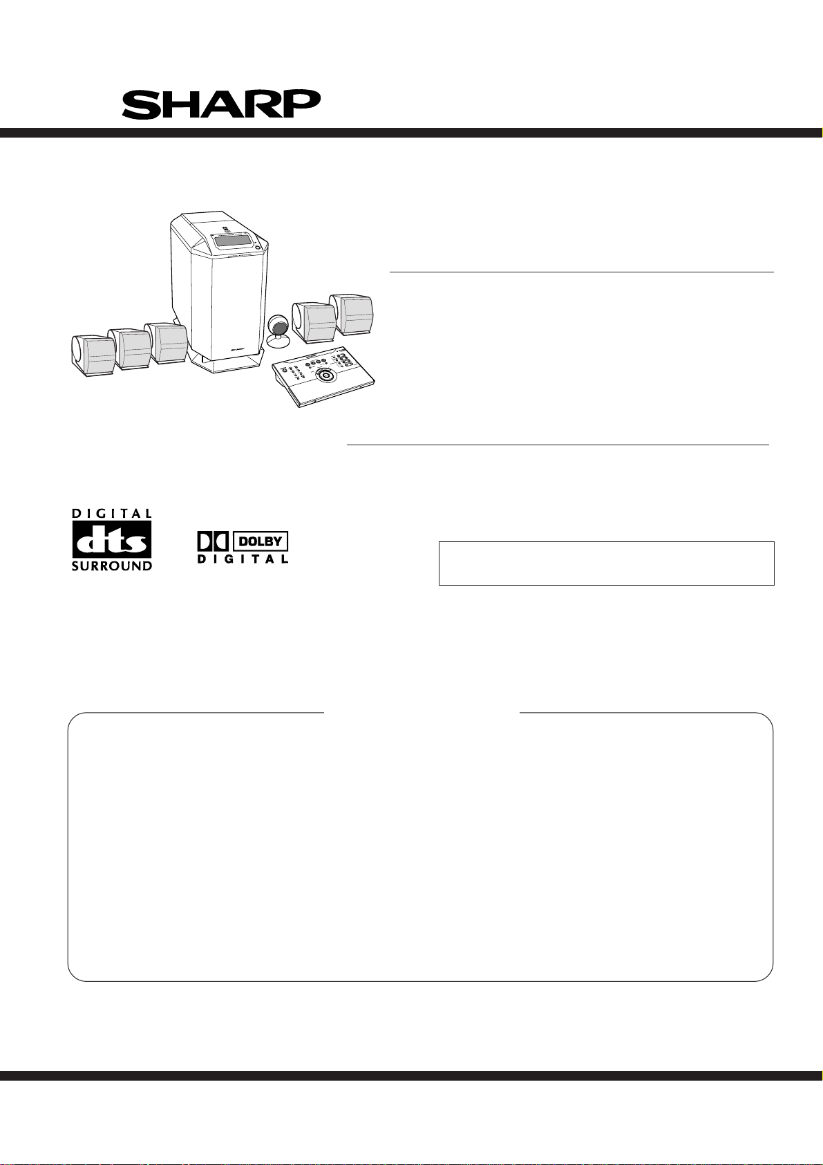
HT-CN300 Home Cinema Command consisting of HT-CN300 (main
unit), CP-CN300F (front speakers), CP-CN300C (center speaker)
and CP-CN300R (surround speakers).
HOME CINEMA COMMAND
MODEL HT-CN300(BK)
HT-CN300 Home Cinema Command consisting of HT-CN300 (main unit),
CP-CN300F (front speakers), CP-CN300C (center speaker) and CP-CN300R
(surround speakers).
• In the interests of user-safety the set should be restored to its
original condition and only parts identical to those specified be
used.
CONTENTS
Page
IMPORTANT SERVICE NOTES (FOR U.S.A. ONLY)....................................................................................................... 2
SPECIFICATIONS ............................................................................................................................................................. 3
NAMES OF PARTS ........................................................................................................................................................... 4
DISASSEMBLY.................................................................................................................................................................. 6
ADJUSTMENT ................................................................................................................................................................... 8
NOTES ON SCHEMATIC DIAGRAM ................................................................................................................................ 9
TYPES OF TRANSISTOR AND LED................................................................................................................................. 9
BLOCK DIAGRAM ........................................................................................................................................................... 10
SCHEMATIC DIAGRAM .................................................................................................................................................. 14
VOLTAGE ........................................................................................................................................................................ 31
WIRING SIDE OF P.W.BOARD....................................................................................................................................... 32
FUNCTION TABLE OF IC................................................................................................................................................ 38
FL DISPLAY..................................................................................................................................................................... 44
REPLACEMENT PARTS LIST/EXPLODED VIEW
PACKING OF THE SET (FOR U.S.A. ONLY)
SHARP CORPORATION
This document has been published to be used
for after sales service only.
The contents are subject to change without notice.
Page 2

HT-CN300
IMPORT ANT SER VICE NOTES (FOR U.S.A. ONLY)
BEFORE RETURNING THE AUDIO PRODUCT
(Fire & Shock Hazard)
Before returning the audio product to the user, perform the
following safety checks.
1. Inspect all lead dress to make certain that leads are not
pinched or that hardware is not lodged between the chassis
and other metal parts in the audio product.
2. Inspect all protective devices such as insulating materials,
cabinet, terminal board, adjustment and compartment covers
or shields, mechanical insulators etc.
3. To be sure that no shock hazard exists, check for leakage
current in the following manner.
* Plug the AC line cord directly into a 120 volt AC outlet.
* Using two clip leads, connect a 1.5 kohm, 10 watt resistor
paralleled by a 0.15 µF capacitor in series with all exposed
metal cabinet parts and a known earth ground, such as
conduit or electrical ground connected to earth ground.
* Use a VTVM or VOM with 1000 ohm per volt, or higher,
sensitivity to measure the AC voltage drop across the
resistor (See diagram).
* Connect the resistor connection to all exposed metal parts
having a return path to the chassis (antenna, metal cabinet,
screw heads, knobs and control shafts, escutcheon, etc.)
and measure the AC voltage drop across the resistor.
VTVM
AC SCALE
1.5 kohms
10 W
0.15 µF
TO EXPOSED
TEST PROBE
METAL PARTS
All check must be repeated with the AC line cord plug connection
reversed.
Any reading of 0.3 volt RMS (this corresponds to 0.2 milliamp.
AC.) or more is excessive and indicates a potential shock
hazard which must be corrected before returning the audio
product to the owner.
CONNECT TO
KNOWN EARTH
GROUND
– 2 –
Page 3
FOR A COMPLETE DESCRIPTION OF THE OPERATION OF THIS UNIT, PLEASE REFER
TO THE OPERATION MANUAL.
SPECIFICA TIONS
HT-CN300
HT-CN300 (Except for Canada)
General
Power source
Power consumption
Dimensions
Weight
Terminals
AC 120 V, 60 Hz
195 W
Width: 9-1/8" (230 mm)
Height: 14-7/8" (377 mm)
Depth: 15-3/4" (400 mm)
24.3 lbs. (11.0 kg)
Front speakers, Center speaker and Surround speakers:
6 ohms
Monitor output: S-video/video
Video output (Video 1): RCA type
Audio output (Video 1): RCA type (L/R)
Video input (Video 1): RCA type
Audio input (Video 1): RCA type (L/R)
Audio input (Auxiliary): RCA type (L/R)
Video input (Video 2): RCA type
S-video input (DVD): S-terminal
Video input (DVD): RCA type
Audio input (Video 2): RCA type (L/R)
Digital input (DVD): Optical
Digital input (DVD): Coaxial
Amplifier
Power output (FTC)
Rated power output
30 watts minimum RMS per channel into 6 ohms from 200
Hz to 20 kHz, 10 % total harmonic distortion
Front: 30 W + 30 W (10% T.H.D, 1 kHz)
Center: 30 W (10% T.H.D, 1 kHz)
Surround: 30 W + 30 W (10% T.H.D, 1 kHz)
Subwoofer: 30 W (10% T.H.D, 100 Hz)
Tuner
Frequency range
CP-CN300F/CP-CN300C/CP-CN300R (Except for Canada)
Type
Maximum input power
Rated input power
Impedance
Dimensions
Weight
Subwoofer (Except for Canada)
Type
Maximum input power
Rated input power
Impedance
FM: 87.5 - 108 MHz
AM: 530 - 1,720 kHz
Full Range Speaker System (Magnetic shield)
3-1/8" (80 mm) speaker
60 W
30 W
6 ohms
Width: 4-1/8" (104 mm)
Height: 4-3/8" (110 mm)
Depth: 4-7/8" (123 mm)
1.8 lbs. (0.8 kg)/each
Subwoofer System (Magnetic shield)
6-1/4" (160 mm) Woofer
60 W
30 W
6 ohms
HT-CN300 (For Canada)
General
Power source
Power consumption
Dimensions
Weight
Terminals
AC 120 V, 60 Hz
195 W
Width: 230 mm (9-1/8")
Height: 377 mm (14-7/8")
Depth: 400 mm (15-3/4")
11.0 kg (24.3 lbs.)
Front speakers, Centre speaker and Surround speakers:
6 ohms
Monitor output: S-video/video
Video output (Video 1): RCA type
Audio output (Video 1): RCA type (L/R)
Video input (Video 1): RCA type
Audio input (Video 1): RCA type (L/R)
Audio input (Auxiliary): RCA type (L/R)
Video input (Video 2): RCA type
S-video input (DVD): S-terminal
Video input (DVD): RCA type
Audio input (Video 2): RCA type (L/R)
Digital input (DVD): Optical
Digital input (DVD): Coaxial
Amplifier
Rated power output
Front speakers:
RMS: 60 W (30 W + 30 W) (10 % T.H.D., 1 kHz)
Centre speaker:
RMS: 30 W (10 % T.H.D., 1 kHz)
Surround speakers:
RMS: 60 W (30 W + 30 W) (10 % T.H.D., 1 kHz)
Subwoofer:
RMS: 30 W (10 % T.H.D., 100 Hz)
Tuner
Frequency range
CP-CN300F/CP-CN300C/CP-CN300R (For Canada)
Type
Maximum input power
Rated input power
Impedance
Dimensions
Weight
Subwoofer (For Canada)
Type
Maximum input power
Rated input power
Impedance
FM: 87.5 - 108 MHz
AM: 530 - 1,720 kHz
Full Range Speaker System (Magnetic shield)
80 mm (3-1/8") Speaker
60 W
30 W
6 ohms
Width: 104 mm (4-1/8")
Height: 110 mm (4-3/8")
Depth: 123 mm (4-7/8")
0.8 kg (1.8 lbs.)/each
Subwoofer System (Magnetic shield)
160 mm (6-1/4") Woofer
60 W
30 W
6 ohms
Specifications for this model are subject to change without
prior notice.
– 3 –
Page 4
HT-CN300
HT-CN300
Main unit (with subwoofer)
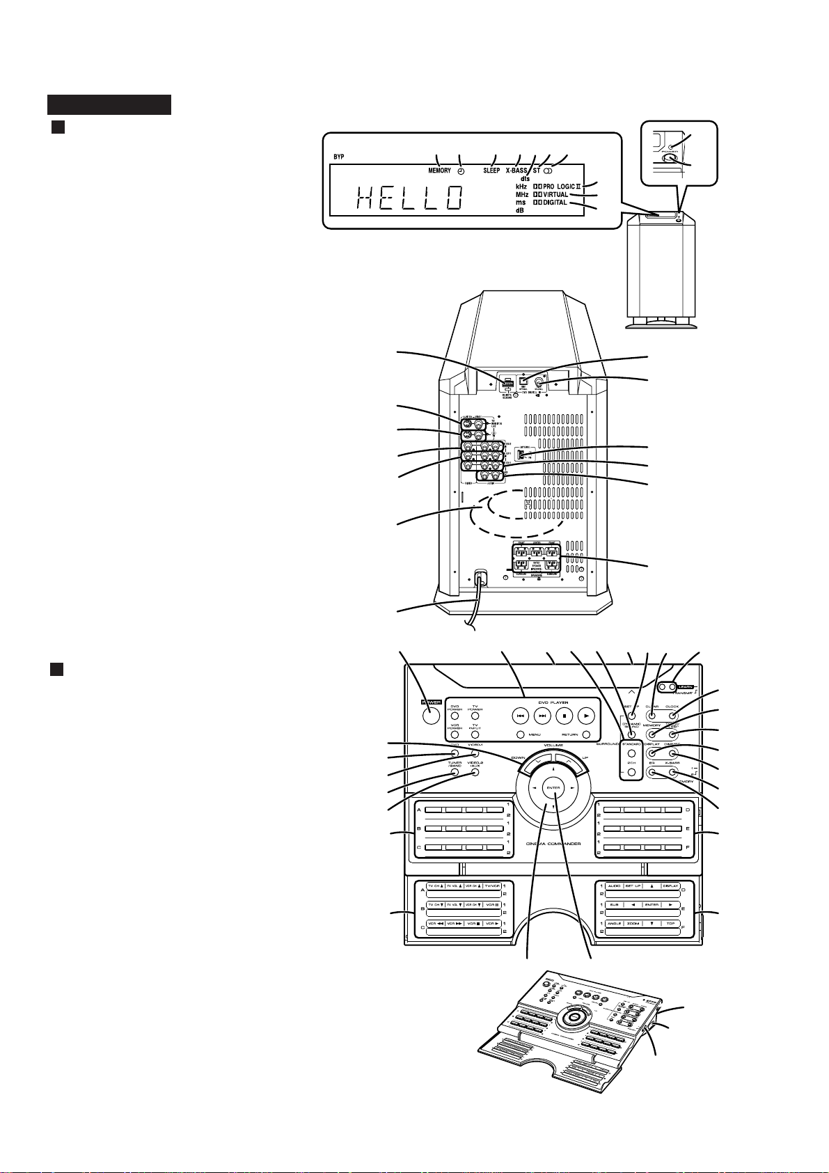
1. Memory Indicator
2. Timer Play Indicator
3. Sleep Indicator
4. Extra Bass Indicator
5. Digital Theater System Indicator
6. FM Stereo Mode Indicator
7. FM Stereo Receiving Indicator
8. Dolby Pro Logic II Indicator
9. Dolby Virtual Indicator
10. Dolby Digital Indicator
11. Power Indicator
12. Power Button
13. Remote Control Sensor Jack
14. TV Monitor Output Jacks
15. DVD Video Input Jacks
16. Video and Audio Input Jacks (VIDEO 2)
17. Video and Audio Input Jacks (VIDEO 1)
18. Subwoofer
19. AC Power Cord
20. DVD Optical Digital Audio Input Jack
21. DVD Coaxial Digital Audio Input Jack
22. FM/AM Loop Antenna Jack
23. Video and Audio Output Jacks (VIDEO 1)
24. Auxiliary Audio Input Jacks
25. Speaker Terminals
NAMES OF P ARTS
12 345867
13
14
15
16
17
18
Back
11
12
9
10
Front
20
21
22
23
24
Remote control
1. Power Button
2. Operation Buttons for Other Equipment
3. Remote Control Transmitter
4. Sound Mode Select Buttons
5. Dynamic Sound Select Button
6. Remote Control Sensor for Learn Function
7. Speaker Set Up Button
8. Clear Button
9. Learn Indicators
10. Volume Up and Down Buttons
11. DVD Button
12. Video-1 Button
13. Tuner/Band Button
14. Video-2/Auxiliary Button
15. Memory 1/2 Buttons for Other Equipment
16. Label Sealing Area
17. Clock Button
18. Memory Button
19. Timer/Sleep Button
20. Display Button
21. Dimmer Button
22. Extra Bass/Demo Mode Button
23. Equalizer Mode Selector Button
24. Cursor Button
25. Enter Button
26. Learn/Transmit Selector Switch
27. 3.6 V DC Input Jack
28. Memory 1/2 Selector Switch
10
11
12
13
14
15
16
19
25
1
256
34
78 9
17
18
19
20
21
22
23
15
16
24 25
26
27
28
– 4 –
Page 5
HT-CN300
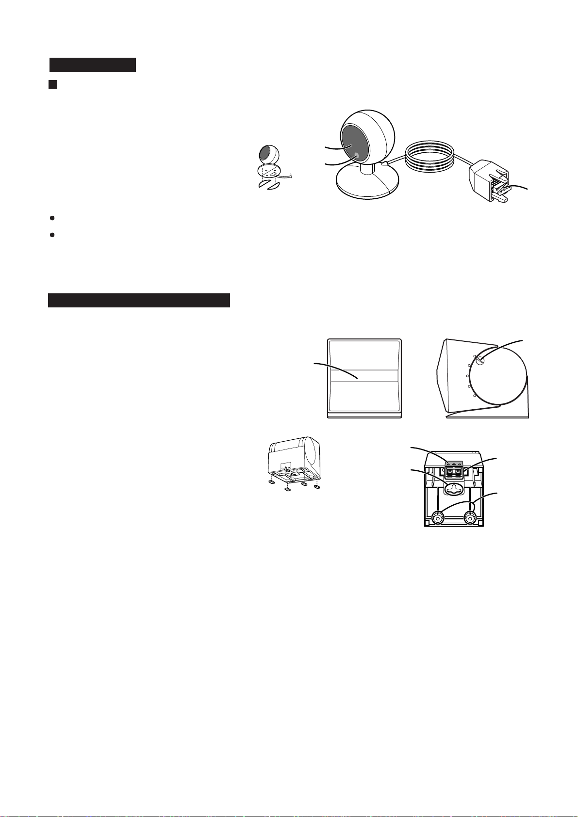
Remote control sensor
1. Remote Sensor
2. Remote Control Indicator
3. Remote Sensor Connection Plug
HT-CN300
Double-sided tape for remote control sensor:
You can fix the remote control sensor with the supplied tape.
Caution:
Carefully choose where you place the remote control sensor as the tape adhesive
may damage or peel the surface coating when the tape is removed.
Never locate the remote control sensor in an unstable place. Otherwise it may fall.
Note:
Fix the remote control sensor on a flat surface.
CP-CN300F/CP-CN300C/CP-CN300R
1. Full-Range Speaker
2. Angle Adjusting Lever
3. Label indication
Front Speaker (right): Red
Front Speaker (left): White
Center Speaker: Green
Surround Speaker (right): Gray
Surround Speaker (left): Blue
4. Mounting Slot
5. Speaker Terminals
6. Mounting Screw Holes
1
1
2
3
Front Side
2
Speaker cushion:
Attach the cushions to the bottom of the speakers to prevent
them from sliding.
3
Bottom
5
4
6
– 5 –
Page 6
HT-CN300
DISASSEMBLY
Caution on Disassembly
Follow the below-mentioned notes when disassembling
the unit and reassembling it, to keep it safe and ensure
excellent performance:
1. Be sure to remove the power supply plug from the wall
outlet before starting to disassemble the unit.
2. Take off nylon bands or wire holders where they need to
be removed when disassembling the unit. After servicing
the unit, be sure to rearrange the leads where they were
before disassembling.
3. Take sufficient care on static electricity of integrated
circuits and other circuits when servicing.
HT-CN300
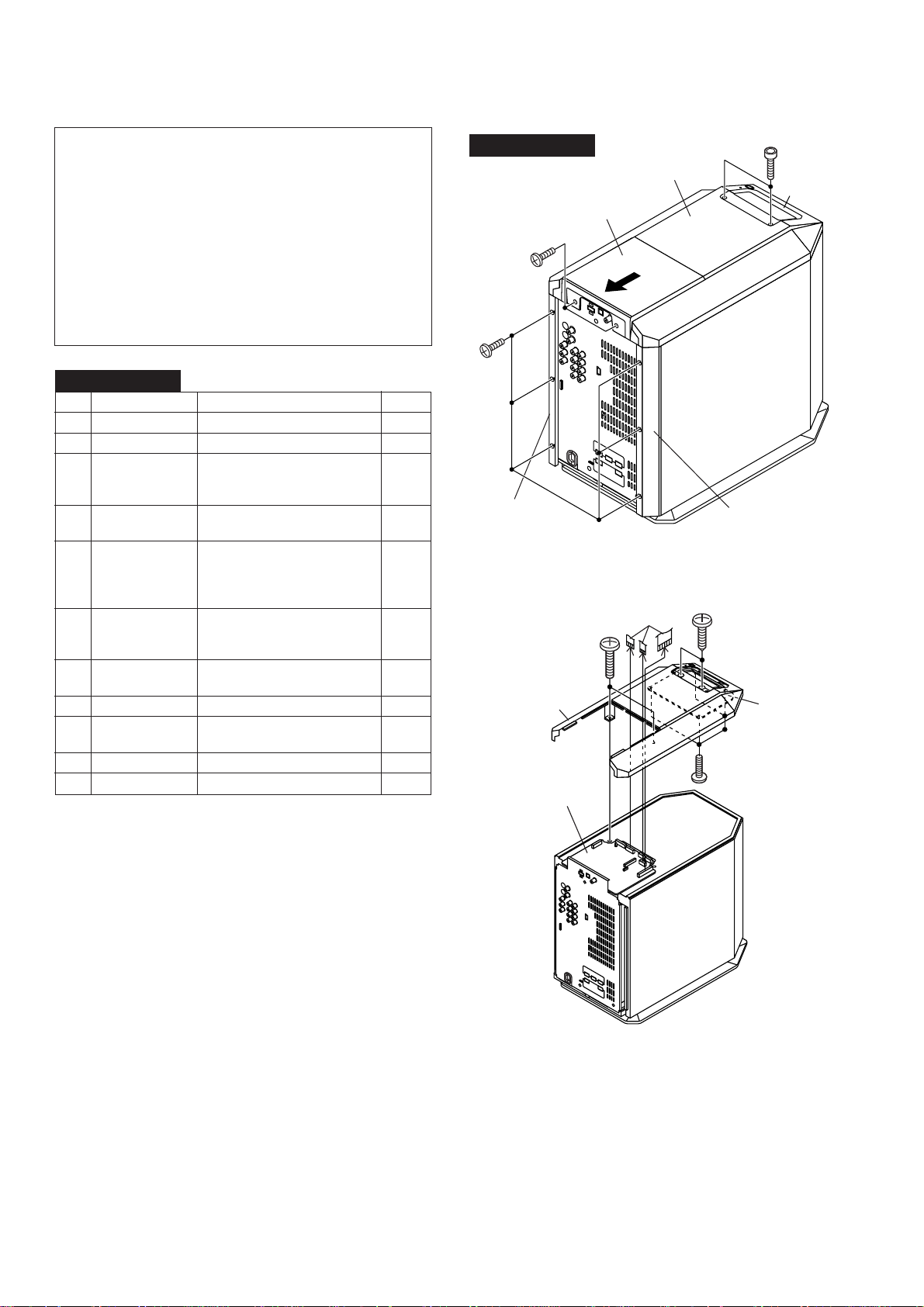
STEP REMOVAL PROCEDURE FIGURE
1 Top Cover B 1. Screw ...................... (A1) x2 6-1
2 LCD Cover 1. Hexagon Screw ...... (B1) x2 6-1
3 Top Cover A/ 1. Screw ...................... (C1) x4 6-2
LCD PWB 2. Flat Cable ............... (C2) x3
3. Screw ...................... (C3) x4
4 Back Cover L/R/ 1. Screw .................... (D1) x25 6-1, 7-1
Rear Panel
5 DSP PWB 1. Screw ...................... (E1) x2 7-2
2. Socket ..................... (E2) x1
3. Flat Cable ............... (E3) x4
4. PWB Holder ............ (E4) x2
6 Subwoofer Stand/ 1. Screw .......................(F1) x4 7-2
PWB Unit 2. Screw .......................(F2) x2
3. Socket ......................(F3) x1
7 Video PWB 1. Screw ...................... (G1) x3 7-3
2. Socket ..................... (G2) x2
8 Audio PWB 1. Screw...................... (H1) x2 7-3
9
AMP. PWB
10 Speaker PWB 1. Screw ...................... (K1) x1 7-3
11 Subwoofer 1. Screw ....................... (L1) x4 7-2
1. Screw ....................... (J1) x6 7-3
2. Socket ...................... (J2) x4
HT-CN300
(A1)x2
ø3x8mm
(D1)x6
ø3x8mm
Back Cover R
(C1)x2
ø4x20mm
Top Cover A
DSP PWB
Top Cover B
Top Cover A
Figure 6-1
(C2)x3
(B1)x2
ø2.5x12mm
LCD Cover
Back Cover L
(C1)x2
ø4x12mm
LCD PWB
(C3)x4
ø3x8mm
– 6 –
Figure 6-2
Page 7
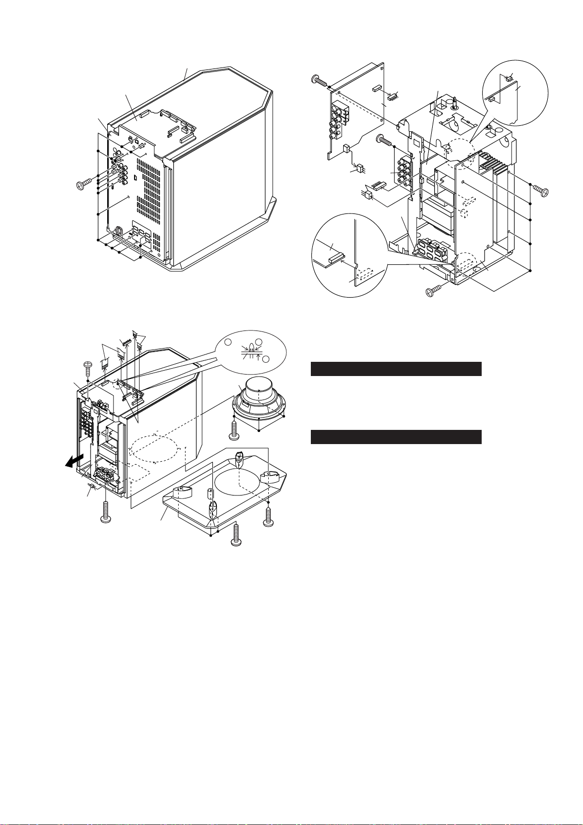
HT-CN300
Rear Panel
(D1)x19
ø3x8mm
(E1)x2
ø3x8mm
DSP PWB
(E3)x2
DSP PWB
(E2)x1
Subwoofer Box
Figure 7-1
(E3)x2
Push
1 Push1
DSP PWB
Subwoofer
(G1)x3
ø3x8mm
(G2)x1
Tuner PWB
(J2)x1
Tuner
PWB
Video
PWB
(H1)x2
ø3x8mm
(G2)x1
Audio
PWB
(J1)x6
ø3x8mm
(J2)x2
Speaker
PWB
Speaker
PWB
AMP.
PWB
AMP.
(J2)x1
(K1)x1
ø3x8mm
PWB
Figure 7-3
Pull
2
CP-CN300F/CP-CN300C/CP-CN300R
These speakers CP-CN300F/CP-CN300C/CPCN300R is
available in assembles only and may not be disassembled.
PWB
Unit
(F3)x1
(F1)x1
ø4x20mm
(E4)x2
Subwoofer Stand
Figure 7-2
(L1)x4
ø4x12mm
(F1)x3
ø4x20mm
(F2)x2
ø4x16mm
Remote control sensor
This Remote control sensoe is available in assembles only
and may not be disassembled.
– 7 –
Page 8
HT-CN300
TP302
TP301
T306
VR351
FM MUTE LEVEL
T302
T351
R357
FE301
R381
CNP301
AM/FM
ANTENNA
AM BAND
COVERAGE fL
AM IF
AM TRACKING
fL
TUNER PWB
8
ADJUSTMENT
TUNER SECTION
fL: Low-range frequency
fH: High-range frequency
••
•
AM IF/RF
••
Signal generator: 400 Hz, 30%, AM modulated
Test Stage Frequency Frequency
Display
AM IF 450 kHz 1,720 kHz T351 *1
AM Band — 530 kHz (fL): T306 *2
Coverage 1.3 ± 0.1 V
AM Tracking 990 kHz 990 kHz (fL): T302 *1
*1. Input: Antenna Output: TP302
*2. Input: Antenna Output: TP301
• FM IF
Notes:
1: Description of the "FM IF Adjustment" is not carried on this
Manual. It is because the IF coil in the FM front end section
has been best adjusted in the factory so that its further
adjustment is not needed at the field. When replacing the
FM front end assembly, no adjustment is needed either.
2: The parts in the FM front end section are prepared in a
complete unit, so you can't obtain each part individually.
Setting/
Adjusting
Parts
Instrument
Connection
OSD SECTION
1: Connect all cables.
2: Power ON
3: Video input (DVD IN or VIDEO 1-IN or VIDEO 2-IN) :NTSC
Signal.
4: Adjust Vfc with rotated of TC432. Vfc range : 2.65 V - 2.75V
(Chick with DC voltmeter, connect (+) of DC voltmeter to pin
26 of IC401, connect (-) of DC voltmeter to pin 2 of
CNP431).
Figure 8-1 TUNER ADJUSTMENT POINTS
VIDEO PWB
CNP431
TC432
26
IC401
Vcf
(2.65 V - 2.75 V)
Figure 8-2 OSD. ADJUSTMENT POINTS
C453
R522
GND
– 8 –
Page 9
NOTES ON SCHEMATIC DIAGRAM
• Resistor:
To differentiate the units of resistors, such symbol as K and
M are used: the symbol K means 1000 ohm and the symbol
M means 1000 kohm and the resistor without any symbol is
ohm-type resistor. Besides, the one with “Fusible” is a fuse
type.
• Capacitor:
To indicate the unit of capacitor, a symbol P is used: this
symbol P means pico-farad and the unit of the capacitor
without such a symbol is microfarad. As to electrolytic
capacitor, the expression “capacitance/withstand voltage”
is used.
(CH), (TH), (RH), (UJ): Temperature compensation
(ML): Mylar type
(P.P.): Polypropylene type
• Schematic diagram and Wiring Side of P.W.Board for this
model are subject to change for improvement without prior
notice.
HT-CN300
• The indicated voltage in each section is the one measured
by Digital Multimeter between such a section and the chassis with no signal given.
1. In the tuner section,
indicates AM
indicates FM stereo
2. In the power section, a tape is being played back.
• Parts marked with “ 1 ” ( ) are important for
maintaining the safety of the set. Be sure to replace these
parts with specified ones for maintaining the safety and
performance of the set.
REF. NO DESCRIPTION POSITION
SW678 POWER ON—OFF
FRONT
VIEW
E C B
(S) (G) (D)
(1) (2) (3)
KRC105 M
KRC107 M
KTA1266 GR
KTA1271 Y
KTA1274 Y
KTC3198 GR
KTC3199 GR
KTC3203 Y
2SB1565 F
2SC2878 B
2SD1898
TYPES OF TRANSISTOR AND LED
FRONT
VIEW
B C E
KTC2026 KRA107 S
B
(3)
TOP
VIEW
E
(1)
KRC107 S
C
(2)
FRONT
VIEW
333ID213
EL204GT
EL204HT
– 9 –
Page 10
HT-CN300
-
V
V
F
_
-
-
+
+
+
+
TV
MONITOR
OUT
DVD IN
VTR2 IN
VIDEO
VTR1 IN
VIDEO
VTR1 OUT
VIDEO
VTR2 IN
AUDIO
AM FM
AM TRACKING
T302 T306
J420
J430
J550
CNP301
8
FE301
FM FRONTEND
6 7 2 5 4 3
VCC
AM BAND
COVERAGE
+B3
SWITCHING
5
10
NJM2279D
SWITCH
3
12
1
X352
VT
4.5 MHz
20 1 22 15 16
IC302
LC72131
PLL(TUNER)
FM
Q416
+B4
8
IC405
VIDEO
14
-B2
450 KHz
CF302
OSC
VIDEO DRIVER
12
1
3
5
AM MIX
1232 4 5 9 8 17 13
AM OSC IN
AM RF IN
21 7 18 16 12 14 15
7 9 10 21
IC404
TK15406M
IC404
TK15406M
Q416
MUTE
+B4
8
IC402
NJM2279D
VIDEO
SWITCH
14
-B2
CF303
CF303
IC303
LA1832S
FM IF DET ./FM MPX./AM IF
STEREO
11
FM/AM
MO/ST
10
FM/AM
OUT
AM IF
3 4 5 6
CE0
DATA
16
CV OUT
18
CV IN
10.7 MHz
CF303
GND
FM+B
FM DET
MPX IN FM/AM R L
DO
CLK
17
+B4
30
2
IC401
LC74763
OSD IC
OSD CS
DATA
CLK
3
8
9
10
X531
456 KHz
VCO
MO/ST
X437
14.32 MHz
+B3
+B2
M
+B3
-B2
-B3
+B4
+B5
VTR1 IN
AUDIO
VTR1 OUT
AUDIO
VIDEO/AUX IN
AUDIO
VTR2 IN
VTR1 IN
VTR1 OUT
VIDEO/AUX IN
TUNER L/R
DSP SECTION
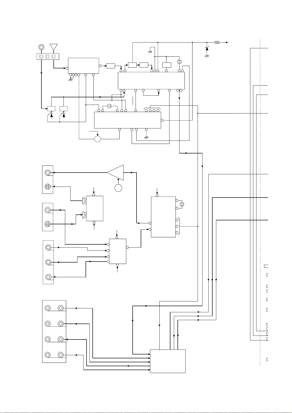
Figure 10 BLOCK DIAGRAM (1/4)
– 10 –
SURROUND L /R
CENTER/SUBWOOFER
MAIN L/R
+B6
+B7
Page 11
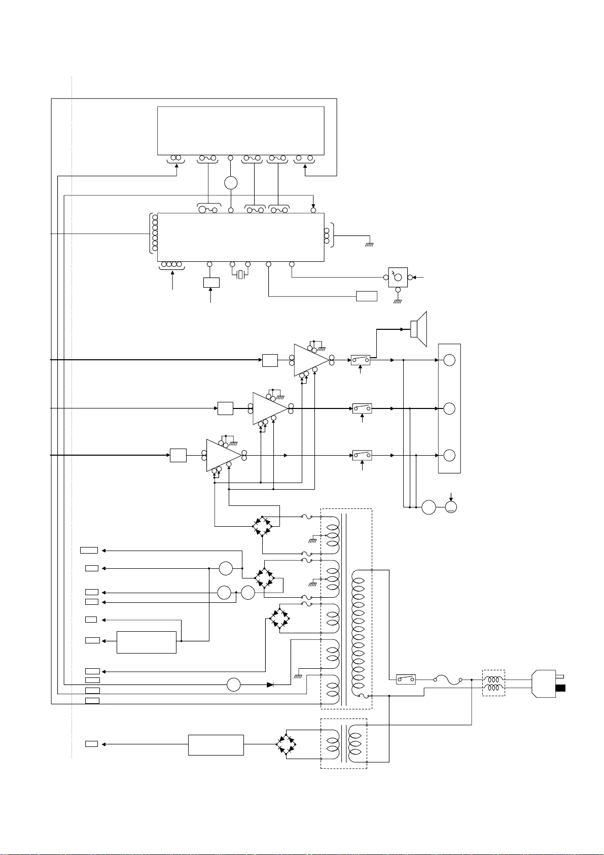
FL690
FL DISPLAY
HT-CN300
12 3534
114 2413 3225
12
VF1 VF2
Q691
56
17
18
8
9
20
19
OSD CS
CLK
DATA
CEO
CE1
CE2
DO
1 163446
+B7
100
93
SYSTEM MICROCOMPUTER
RESET KEY_O
10 11 12
Q682
IC602
8091 7178
92 79
IC601
UPD780206
REMOCON
33 39
X611
4.1943MHz
+B7
20ATT
Q210
Q220
20ATT
Q240
Q230
10
IC201
13
POWER AMP
8
LM4766
15
2
+B1
20ATT
Q240
Q230
IC202
13
POWER AMP
8
LM4766
15
2
5
L
1
3
R
4
-B1
D101
IC203
13
POWER AMP
8
LM4766
2
10
5
L
1
3
R
4
F101
8A/125V
10
15
40
25
13
5
C
1
3
W
4
MAIN POWER
TRANSFORMER
RY250
T100
IC10
REMOTE SENSOR
12
SW678
+B2
RY230
+B2
RY210
+B2
3
FAN MOTOR
Q202
DRIVER
+B7
SUBWOOFER
J201
CENTER
SURROUND
MAIN
SPEAKER TERMINAL
+B6
M200
M
FAN MOTOR
+B2
+B3
-B2
-B3
+B4
+B5
+B6
+B7
M_12V
+9V
-5V
-9V
+5V
+3V3
FANB
-VP
VF1
VF2
+5V
IC103
BA033T
VOLTAGE
REGULATOR
Q150
Q132
IC501
KTA7805AP1
CONSTANT VOLTAGE
REGULATOR
F102
8A/125V
D114
F111
1.25A/125V
F112
1.25A/125V
D123
F121
800mA/125V
D124
D112
Q112Q113
D111
D113
D121
D122
D131
D522
D524
D525
D523
T501
SUB POWER TRANSFORMER
Figure 11 BLOCK DIAGRAM (2/4)
– 11 –
RY511
F511
4A/125V
L511
LINE
FILTER
AC POWER
SUPPLY CORD
AC 120 V/60 Hz
Page 12
HT-CN300
SDA/CDTI
K
1
Q
Q
Q
Q
IC701
TVHC574T
LATCH
1
OE
2
D0
3
D1
4
D2
5
D3
6
D4
7
D5
8
D6
9
D7
10
GND
A0
19
A1
18
A2
17
A3
16
A4
15
A5
14
A6
13
A7
3
A8
2
A9
31
A10
1
A11
12
A12
4
A13
A14
5
A15
11
A16
10
A17
6
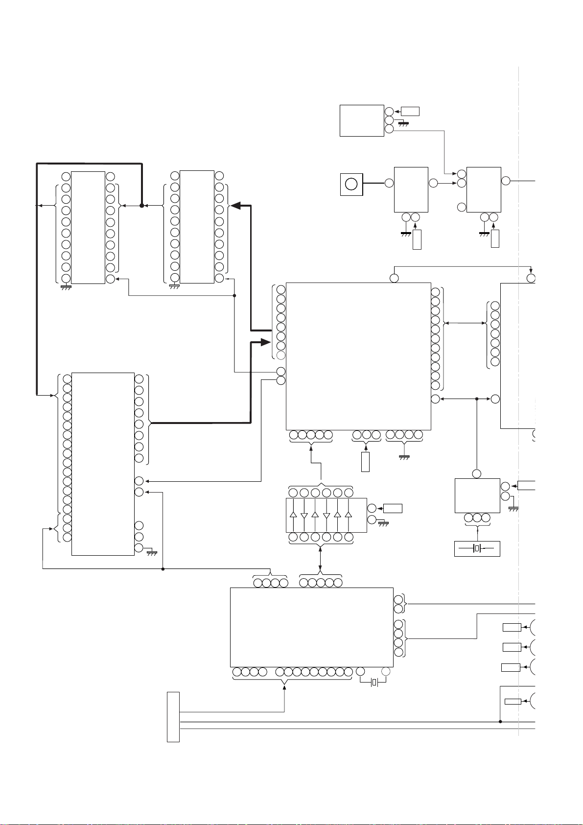
DISPLAY SECTION
20
VCC
19
O0
18
O1
17
O2
16
O3
15
O4
14
O5
13
O6
12
O7
CK
11
IC703
MX27L212
EPROM
GND
FROM
2120
O0
22
O1
23
O2
25
O3
26
O4
27
O5
28
O6
29
O7
32
OE
30
CE
8
VCC
9
VPP
24
IX0489A
SYSTEM
MICROCOMPUTER
IC702
TVHC574T
LATCH
1
OE
VCC
2
D0
3
D1
4
D2
5
D3
6
D4
7
D5
8
D6
9
D7
10
GND
IC710
20
19
O0
18
O1
17
O2
16
O3
15
O4
14
O5
13
O6
12
O7
CK
11
IC704
74HC07AF
BUFFER AMP.
FLD_SDATA
FLD_SCK
2341 202223 25262724 78
SPDIF COAX IN
8
D7
9
D6
10
D5
11
D4
14
D3
15
D2
16
D1
17
D0
RD
4
EXTMEM
21
RESET
36 18 19 20
2
1
65
474548
DSP_UC16
ROM
DSP_UC15
DSP_UC17
FLD_RESET
FLD_CS
RXIN
STD_LED
DD_LED
CON707
CS
SCDOUT
INTREQ
SCDIN
6
3
6
8
45
39 38 37 36 35
DSP_RESET
DSP_CS
DSP_SCLK
DSP_SCOUT
AAC_LED
DTS_LED
DPL_LED
VIR_LED
IC709
GP1F32R
DIGITAL IN
GND
VOUT
IC706
CS493292
DSP
VD1
123
12
+2V5
+B5B
109
VCC
GND
131211
DSP_SCDIN
C_SP_RLY
S_MUTE
POWER
S_SP_RLY
W_SP_RLY
13
72
8.38 MHz
1
VCC
2
3
TC7WU04U
1
VD3
VD2
+3V3
14
7
SCL
SDA
15
XL1
INVERTER
3
DGND1
+B4A
+5V
IC721
2
3Y1A
GND
VCC
167
+B5A
+3V3
MCLK
44
SCLK
LRCLK
AUDAT0
AUDAT1
AUDAT2
SCLKN1
AGND
DGND3
352
24
43
42
41
40
39
25
26
27
28
22
30
XMT958
LRCLKN1
SDATAN2
SCLKN22
SDATAN1
SDATAN1
DGND2
13
IC707
TC7WU04U
DUAL2-INPUT
NAND GATE
+B5
29
30
82F_SP_RLY
81
80
79
IC722
TC74153
MULTIPLEXER
1I1
6
1I0
5
S0
14
3
1A
1
XL1
12.288 MHz
7
1Y
GND
VCC
7
16
+3V3
7
MCKO
8
LRCK
9
BICK
10
STDO
11
SDTI1
12
SDTI2
SDTI3
11
XTI/EXTCL
2
3Y
VCC
8
GND
4
1Y
3A
7
6
+B7A
+3V3
+B5A
+3V3
SWITCHING
+B4A
SWITCHING
+B5A
37
RX4
+B5
+3V3
+B3A
+8V
+5V
Figure 12 BLOCK DIAGRAM (3/4)
– 12 –
Page 13
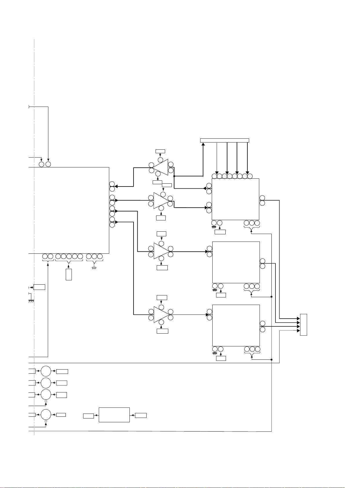
FROM AUDIO SECTION
HT-CN300
41
37
RX2
RX4
KO
CK
CK
DO
TI1
TI2
TI3
I/EXTCLK
+B5
+3V3
7A
V3
B3A
8V
V3
ITCHING
B4A +B4
5V +5V
ITCHING
AK4586VQ
ADC/DAC/DIR
CONVERTER
SDA/CDTI
SCL/CCLK
+B7
+5V
Q703
+B3
+9V
Q704
+B5B5A
Q701
+3V3
Q721
IC708
DVDD1
TVDD2
35 22 34
PVDD
+B4 +5V
ADD
23
VREFH
4213617 18
+B5B
+2V5
ROUT1
LOUT1
ROUT2
LOUT2
ROUT3
LOUT3
DVSS1
PVSS
RIN
LIN
AVSS
REGULATOR
33
32
31
30
29
28
27
26
IC705
PQ25EZ
VOLTAGE
IC718
NJM4580M
OPE AMP.
IC716
NJM4580M
OPE AMP.
+B5
+3V3
-B3
+B3A
+8V
8
4
-9V
+B3A
+B3A
-9V
-B3
+8V
-9V
-B3
+8V
-9V
-B3
4
8
4
8
4
3
5
+8V
+B3A
8
1
7
NJM4580M
OPE AMP.
1
7
NJM4580M
OPE AMP.
1
7
ANALOG IN Lch
ANALOG IN Rch
FRONT Lch
FRONT Rch
IC715
SURROUND Lch
SURROUND Rch
IC711
CENTER
WOOFER
1
7
3
5
3
5
3
5
VCR1 OUT
7
18
12
13
3
12
13
3
12
13
3
VCR1 IN
VCR2 IN
IC720
LC75341
AUDIO
PROCESSOR
23
+8V
B3A
LC75341
AUDIO
PROCESSOR
23
+8V
B3A
LC75341
AUDIO
PROCESSOR
23
B3A
+8V
VIDEO/AUX IN
15 161011141213 9
IC713
IC712
TUNER
CLK
24
CLK
CE
24
CLK
24
2
2
CE
21
4
DI
CE
1
21
4
DI
1
TO POWER AMP
SECTION
21
4
DI
2
1
Figure 13 BLOCK DIAGRAM (4/4)
– 13 –
Page 14
HT-CN300
T
AMP. PWB-B3 (1/2)
FM SIGNAL
A
PROTECT
FAN_CONT
POW_LEVEL
22K THERMO
C263
0.001
B
R140
100K
R141
100K
C
R271
2.2K
R270
820
R259
R258
820
0.001
2.2K
C254
R272
100
B
B
R260
C
E
C
E
100
Q260
2SC2878 B
Q250
2SC2878 B
C264
1/50
(N.P.)
C255
1/50
(N.P.)
R261
22K
R273
22K
C265
22/35
(N.P.)
R274 1K
R275 270
R276 22K
R262 1K
R263 220
R264 22K
C256
22/35
IC203
(N.P.)
LM4766T
POWER AMP.
5
2
15
4
10
VEE
GNDA
GNDB
VCCB
VCCA
+INA
8
-INA
7
+INB
13
-INB
12
MuteA
VEE
VccB
MuteB
VEE
GNDA
GNDB
MUTEB6MUTEA
11
OUTA
3
1
OUTB
NC2
NC1
9
14
R282 10K
TERMINAL PWB-B5
IC202
VEE
VEE
2
VCCA
MuteA
VccB
MuteB
5
GNDA
GNDA
GNDB
MUTEB
MUTEA
6
11
R291 10K
LM4766
POWER
4
15
10
VEE
VCCB
GNDB
OUTA
OUTB
NC1
14
AMP.
3
1
NC2
9
D
E
R142
100K
R143
100K
R247
2.2K
C232
0.001
R235
2.2K
C241
0.001
R246
820
R234
0.22
R237 22K
0.22
C236
4.7
C243
22/35
(N.P.)
C234
22/35
R249
22K
R250
1K
R251 220
R252 22K
R238 1K
R239 220
R240
22K
8
+INA
-INA
7
+INB
13
12
-INB
C
Q240
B
2SC2878 B
E
R248
100
C242
1/50
(N.P.)
C
Q230
B
2SC2878 B
E
C233
R236
1/50
100
820
(N.P.)
CNP203
CNS204
BI204
1
2
3
4
5
1
6
2
7
3
8
4
5
6
7
8
C206
C245
0.22
0.22
R253
C207
4.7
R241
C170
100/10
F
FW12
FL_PRIOUT
A_GND
FR_PRIOUT
SR_PRIOUT
A_GND
SL_PRIOUT
CT_PRIOUT
G
CNP711
DSP PWB
P23 12 - F
A_GND
SW_PRIOUT
A_GND
F_RLY
S_RLY
C_RLY
TO
W_RLY
-20DBATT
FAN_CONT
THERMO
PROTECT
POW_LEVEL
CNP122
1
1
2
3
4
5
6
7
8
9
10
11
12
13
14
15
16
17
18
19
19
R144
100K
R145
100K
H
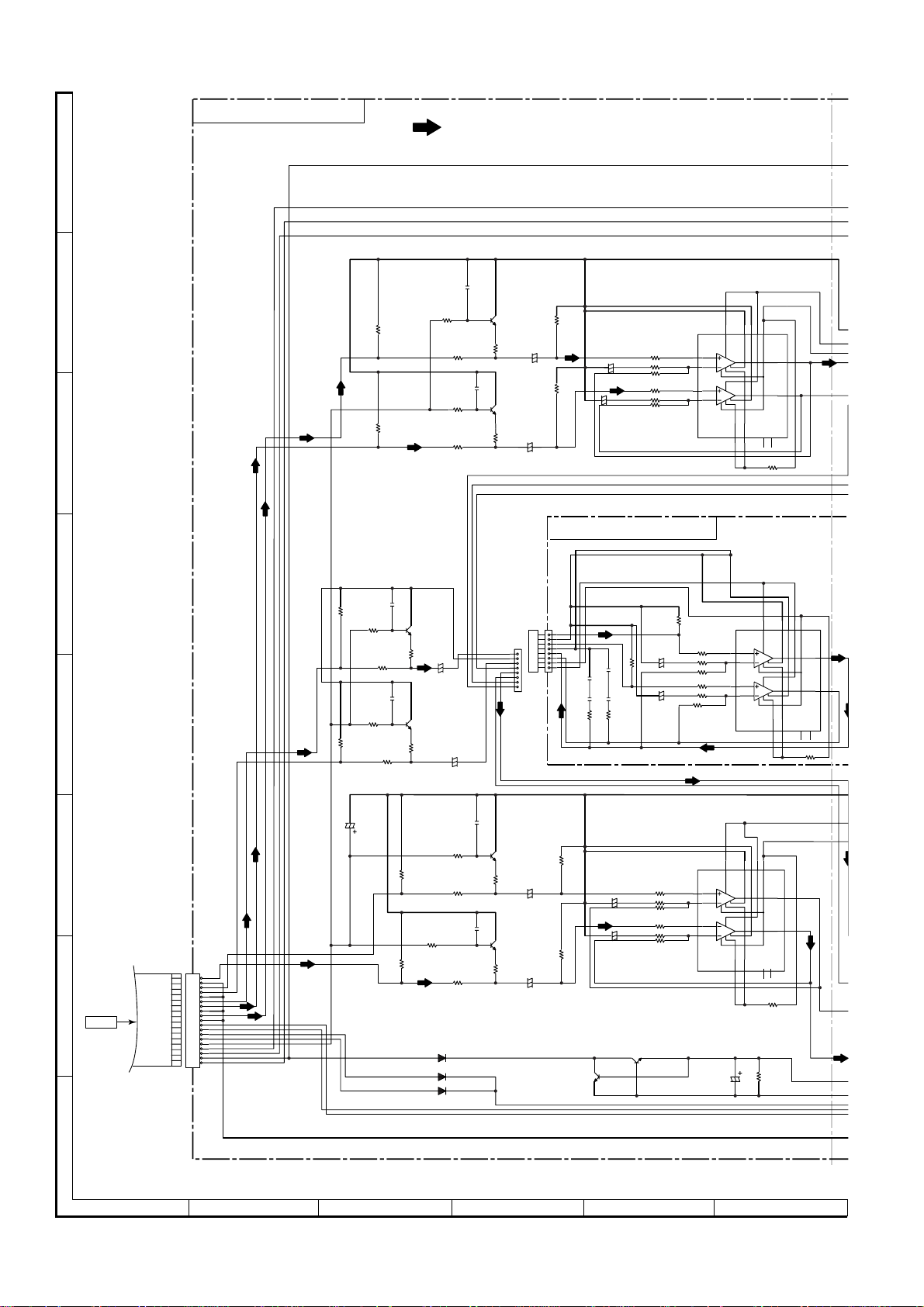
• NOTES ON SCHEMATIC DIAGRAM can be found on page 9.
1
23456
Figure 14 SCHEMATIC DIAGRAM (1/17)
C219
0.001
R223
2.2K
R222
820
C210
0.001
R211
2.2K
R210
820
D272 DS1SS133
D251 DS1SS133
D252 DS1SS133
– 14 –
C
B
E
C
B
E
Q220
2SC2878 B
R224
100
Q210
2SC2878 B
R212
100
C220
1/50
(N.P.)
C211
1/50
R225
22K
R213
22K
Q271
KTC3199 GR
C221
22/35
(N.P.)
C212
22/35
(N.P.)
C
B
E
POWER AMP.
R226 1K
R227 220
R228 22K
R214
R215 220
R216 22K
Q270
KTC3199 GR
EBC
IC201
LM4766T
8
7
1K
13
12
+INA
-INA
+INB
-INB
C272
47/50
2
VCCA
MuteA
VEE
VccB
MuteB
VEE
5
GNDA10GNDB
GNDA
GNDB
MUTEB
6
11
MUTEA
15
4
VEE
VCCB
OUTA
OUTB
NC19NC2
14
R290 10K
R168
56K
3
1
Page 15
HT-CN300
IC202
M4766T
POWER
AMP.
D201
DS1SS133
Q200
KRC107 M
2
1
M200
FAN MOTOR
1
2
M
CNS205
TO
AMP. PWB (2/2)
P24 1 - A
C203
47/50
3
Q203
2SB1565 F
CNP205
1
2
4
5
6
7
8
FANB
FANGND
+B1
-B1
PGND
M_12VA
PGND_A
R208 10
3
C204
100/10
R299
1K
R200
820K
Z201
DZ3.9BSB
R209 22K
D200
DS1SS133
E
C
Q204
KTA1271 Y
B
Z200
DZ5.1BSB
R207 10
R201 1K
R202
220K
R203 2.7K
C200
47/10
R171
10K
DS1SS133
R170
8.2K
B
D170
C
E
Q201
KTC3203 Y
R204
470K
KRC107 M
Q170
B
C201
47/16
C
E
B
DS1SS133
C
KTC3199 GR
E
D171
Q202
DZ6.2BSB
R205
15(1W)
R172
3.9K
Z202
D172
DS1SS133
1
2
OUTA
OUTB
R278
3
0.22
0.22
0.22
C202
C267
0.22
C205
C258
0.22
1
NC2
9
C208
C223
0.22
C209
C214
0.22
0.22
10K
CON201
2
1
SUBWOOFER
10K
R231 10K
R219 10K
R242 10K
R266 10K
J201
SPEAKER TERMINAL
FR_GND
FR
SR_GND
SR
CT_GND
CT
FL_GND
FL
SL_GND
SL
R162
R163
56K
R165
56K
R164
56K
R166
56K
R167
56K
56K
R277 10
R176 10
R175 10
R265 10
R180 10
R297
1K
Q255
KRC105 M
R295
1K
KRC105 M
KRC105 M
R218 10
R229 10
R181 10
E
B
E
B
Q235
R293
1K
B
Q215
C
C
E
C
RY250
D250
DS1SS133
RY230
D230
DS1SS133
RY210
D210
DS1SS133
CON210
R254 10K
1
1
2
2
3
3
4
4
5
5
6
6
7
7
8
8
9
9
10
10
11
11
CON211
SPEAKER PWB-B6
7
8 9 10 11 12
Figure 15 SCHEMATIC DIAGRAM (2/17)
– 15 –
Page 16
HT-CN300
SMUTE(NO USE)
P3
C
D
Y
C
A
B
C
FW7
AC_RLY
D_GND
FUNC_DVD
VREC_MUTE
CLK
V_SW1
DATA
V_SW2
V_MUTE
D
E
OSD_CS1
CON703
DSP PWB
P20 1 - G
P1023P1124P1225P1326P1427P1528P1629P1730P1831P1932P2034F235F1
C623
47/50
R623
12K
Z621
DZ6.2BSB
US5V_1
C625
0.022
S5V_1
C624
0.022
CNP670
1
1
2
3
4
5
6
7
8
9
10
10
TO
R693
33
C693
100/10
R621
R622
47
47
C692
1/50
R654 47K
R653 47K
R652 47K
R651 47K
R650 47K
R649 47K
R648 47K
R647 47K
R646 47K
R645 47K
R644 47K
R643 47K
R642 47K
R641 47K
R640 47K
R639 47K
R685
10K
R686
10K
R665 1K
FUNC_TUNER
R662 1K
R661 1K
R660 1K
R659 1K
R658 1K
R657 1K
R656 1K
R655 1K
80
P12
79
VLOAD
78
P13
77
P14
76
P15
75
P16
74
P17
73
P18
72
P19
71
P20
70
F_SP_RLY
69
C_SP_RLY
68
S_SP_RLY
67
W_SP_RLY
66
AC_RLY
65
LMUTE
64
NO_USE3
63
FUNC_TUNER
62
FUNC_DVD
61
V_REC_MUTE
60
V_SW1
59
V_SW2
58
NTSC/PAL
57
OSD_CS2
56
OSD_CS1
55
OSD_RST
54
AAC/MPEG_LED
53
DPL_LED
52
VIR_LED
51
DTS_LED
V_MUTE
81
83P984P885P786P687P588
P1182P10
MICRO
17P518P619P720P821P922
P4
I
UP
S
EL204GT
F
CNP701
TO
DSP PWB
P20 1 - E
FW6
DD_LED
DSP_POWER_IN
STD_LED
DSP_SMUTE_IN
DTS_LED
G
REM_ACK_LED
VIR_LED
REMCON
DPL_LED
DSP_RST
AAC/MPEG_LED
DSP_RX_IN
DSP_STAND_BY
FLD_SDATA
L_MUTE
NC
VF2
FLD_SCK
-VP
FLD_CS
VF1
CCB_CE1
SW_5V
CCB_CE0
UN_SW_5V
CLK
D_GND
DATA
CCB_CE2
H
CNP640
1
1
2
3
4
5
6
7
8
9
10
11
12
13
14
15
16
NC
17
18
19
20
21
22
23
24
25
26
27
28
29
29
RED
R699 1.5K
R698 300
LED699
LE204HT
GREEN
LED698
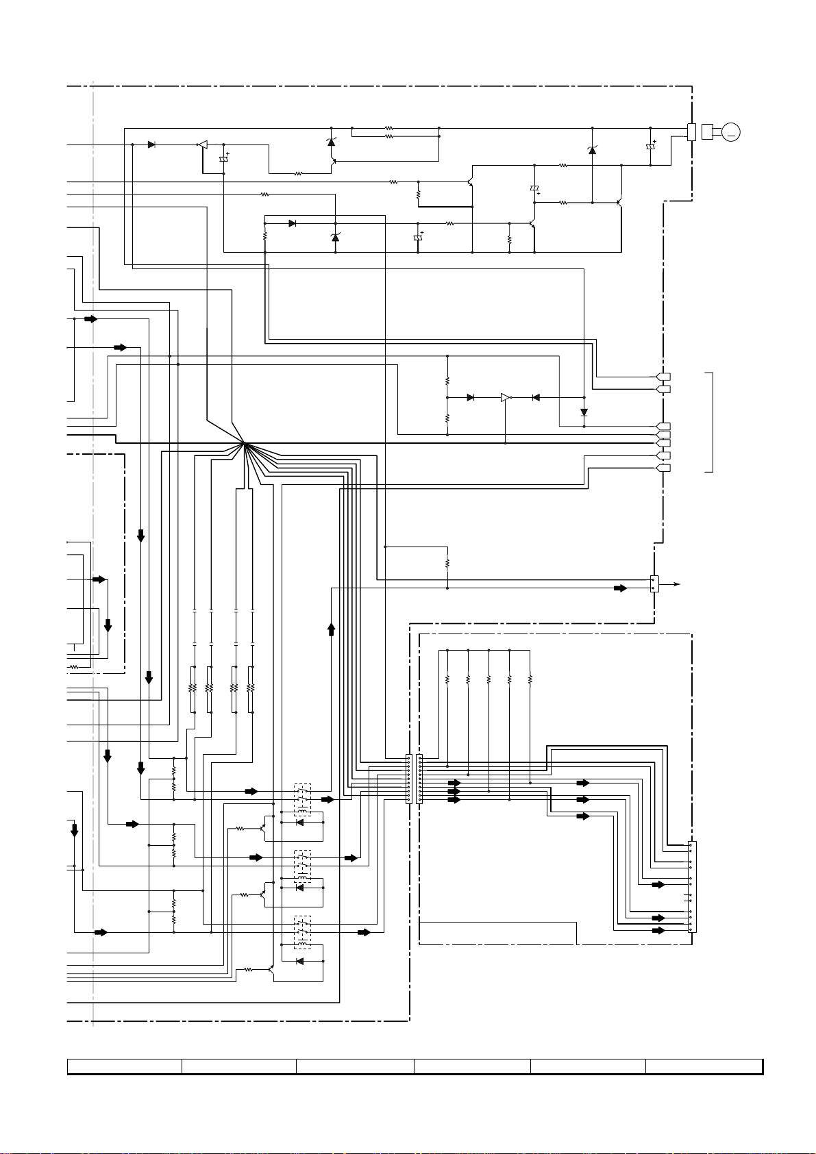
• NOTES ON SCHEMATIC DIAGRAM can be found on page 9.
1
23456
Figure 16 SCHEMATIC DIAGRAM (3/17)
– 16 –
C660
0.022
111213141516171819
GND
10
DD_LED
STD_LED
50
20
VCC
123456789
DSP_POWER_IN
48
49
POWER_ON_LED
STAND_BY_LED
DSP_RST
VDD347DSP_SMUTE_IN
43
44
45
46
IC604
VHC541AF
BUFFER AMP.
Page 17
HT-CN300
29
P18
P1023P1124P1225P1326P1427P1528P16
P17
22
83
P984P885P786P687P588P489P390P291P192G993G894G795G696G597G498G399G2
G610G711G812G913P114P215P316P417P518P619P720P821P9
IC601
UPD780206
SYSTEM
MICROCOMPUTER
FL690 DISPLAY
1F42F34G15G26G37G48G59
RDS_RDCL/KARA_LAC
RDS_RDDA
KRC107 M
R692
100K
100
G1
VDD1
RDS_READY
/MIC_IN
RDS_RESET
-20_ATT
FAN_CONT
CCB_CE0
CCB_CE1
RESET
VPP/IC
VDD2
DATA
CCB_DO
CCB_CE2
FLD_CS
FLD_SCK
NO_USE1
FLD_SDATA
AVSS
POWER_LEVEL
PROTECT
THERMO
TUN_SM
DIST_1
R690
3.3
C690
B
1
R602 1K
2
R603 1K
3
R604 1K
4
R605 1K
5
R606 1K
6
R607 1K
7
R608 1K
8
R609 1K
9
10
11
12
13
14
R615 1K
15
16
R617 1K
17
R618 1K
18
R619 1K
19
R620 1K
20
21
22
23
24
25
R626 1K
26
27
28
29
30
1/50
R691
1K
C600
0.022
R627 1K
R628 1K
R629 1K
R630 1K
C601
1000/6.3
R610 1K
C611
12P(CH)
X611
C612
18P(CH)
R614 10K
R672 10K
R673 10K
R674 10K
R675 10K
CNP601
14
13
12
11
10
FW8
14
-20DBATT
F_RLY
FAN_CONT
C_RLY
9
8
7
6
5
4
3
2
1
CCB_CE0
S_RLY
CLK
W_RLY
DATA
THERMO
CCB_DO
PROTECT
D_GND
POWER_LEVEL
1
CNP708
DSP PWB
P21 12 - F
TO
Q691
C
E
X2
X1
XT2
SPN
CLK
VDD347DSP_SMUTE_IN
DSP_POWER_IN
46
48
IC604
DSP_RST
45
40
42
43
44
VSS41REM_ACK_LED
SMUTE(NO_USE)
POWER_ON_LED
STAND_BY_LED
R635 1K
R667 3.3K
VHC541AF
BUFFER AMP.
DSP_RX-IN_OUT
DSP_STAND_BY
REMCON
37
38
39
R638 1.5K
R637 1.5K
R666 3.3K
2
1
SYS_STOP
36
SW678
R633 1KR678 10K
POWER
DIST_032KEY_133KEY_034AVDD35AVREF
31
R677 10K
R676 10K
R636 10K
IC603
74VHC541AF
C622
4.7/50
111213141516171819
C620
0.022
GND
BUFFER AMP.
10
D681
DS1SS133
D684
D683
DS1SS133
R683
47K
Q682
KRC107 M
C
E
1N4004S
B
D682
DS1SS133
R682
100K
C682
3.3/50
C681
REGULATOR
0.022
BACK-UP
20
VCC
123456789
UN_SW_5V
SW_5V
D685
DS1SS133
C686
0.1/50
C685
0.022
D680
DS1SS133
R680
4.7K
IC602
KA7042AP
VOLTAGE
1
3
2
C680
10/50
DISPLAY PWB-B1
7
8 9 10 11 12
Figure 17 SCHEMATIC DIAGRAM (4/17)
– 17 –
Page 18

HT-CN300
27
A
41
0
1
A
DSP PWB-A1 (1/3)
[1,2,3]
SW5V
[2,3]
UNSW5V
[2]
DG_CNG
[2]
FUNCDVD
B
[2,3]
[1,2,3]
3.3V
DGND
C
D
E
+B +B
1
2
3
4
C738
0.022
DSP_A15
DSP_A14
DSP_A13
DSP_A12
DSP_A11
DSP_A10
DSP_A09
DSP_A08
+B
11
CLK
12
Q7
13
Q6
14
Q5
15
Q4
16
Q3
17
Q2
18
Q1
19
Q0
20
VCC
IC701
TVHC574T
LATCH
GND
+B
IC702
TVHC574T
C736
0.022
10
9
DSP_A07
D7
8
DSP_A06
D6
7
DSP_A05
D5
6
DSP_A04
D4
5
DSP_A03
D3
4
DSP_A02
D2
3
DSP_A01
D1
2
DSP_A00
D0
1
OE
R745
10K
DSP_A07
DSP_A06
DSP_A05
DSP_A04
DSP_A03
DSP_A02
DSP_A01
DSP_A00
DSP_A10
DSP_A11
DSP_A09
DSP_A08
DSP_A13
DSP_A14
DSP_A12
DSP_A07
DSP_A06
DSP_A05
LATCH
11
CLK
12
Q7
13
Q6
14
Q5
15
Q4
16
Q3
17
Q2
18
Q1
19
Q0
20
VCC
C739
0.022
1
A11
2
A9
3
A8
4
A13
5
A14
6
A17
7
PGMB
8
VCC
9
VPP
10
A16
11
A15
12
A12
13
A7
14
A6
15
A5
16
A4
IC703
MX27L212
EPROM
EXTMEMB
IC703
C735
10/16
10
GND
9
DSP_D07
D7
8
DSP_D06
D6
7
DSP_D05
D5
6
DSP_D04
D4
5
DSP_D03
D3
4
DSP_D02
D2
3
DSP_D01
D1
2
DSP_D00
D0
1
OE
C740
10/16
32
31
A10
30
CEB
29
DSP_D07
O7
28
DSP_D06
O6
27
DSP_D05
O5
26
DSP_D04
O4
25
DSP_D03
O3
24
GND
23
DSP_D02
O2
22
DSP_D01
O1
21
DSP_D00
O0
DSP_A00
20
A0
DSP_A01
19
A1
18
DSP_A02
A2
MX27L2000TC
17
DSP_A03DSP_A04
A3
DSP_A[00:15]
+B+B
DSP_D07
R705 10K
DSP_D06
R706 10K
DSP_D05
R707 10K
DSP_D04
R708 10K
DSP_D03
R709 10K
DSP_D02
R710 10K
DSP_D01
R711 10K
DSP_D00
R712 10K
[1]DSP_D[00:07]
+B
C706
22/16
C707
0.1
DSP_D[00:07]
[1]
R704
4.7K
+B
+B
C782
C781
0.1
47/16
PQ025EZ
VOLTAGE
4.7K
R703
DSP_D07
DSP_D06
DSP_D05
DSP_D04
DSP_D03
DSP_D02
DSP_D01
DSP_D00
REGULATOR
3.3K
R702
7
SCCLK
8
D7
9
D6
10
D5
11
D4
12
VD2
13
DGND2
14
D3
15
D2
16
D1
17
D0
+B
DSP_D[00:07]
[1]
+3.3V
5
6
1
VIN
2
VC
VO1
NC
GND
VO2
6
3
4
5
IC705
C731
0.1
3.3K
10K
R701
R735
1
2
3
6
VD1
XMT4WRB5RDB
DGND1
IC706
CS493292
DSP
CSB19SCDOUT20INTB21EXTMEMB22SDATAN123VD324DGND325SCLKN126LRCKNN1
18
R758
330
R757 330
R726 330
R727 100
42
43
44
SCLK
MCLK
LRCLK
[2]
DSP_INTREQ
[2]
[2]
[2]
[2]
[2]
[2]
F
[2]
[2]
DSP_SCDOUT
[2]
[2]
[2]
[2]
DSP_ABOUT
ROM
DSP_UC17
DSP_UC16
DSP_UC15
DSP_RESET
DSP_CS
DSP_SCCLK
DSP_SCDIN
SDA
SCL
7
8
9
10
11
12
13
14
15
16
17
18
19
G
H
• NOTES ON SCHEMATIC DIAGRAM can be found on page 9.
1
23456
Figure 18 SCHEMATIC DIAGRAM (5/17)
IC704
– 18 –
14
1234567
74HC07AF
BUFFER AMP.
+B
C729
10/16
8
910111213
C725
0.022
+B
GND
R713
4.7K
R714
3.3K
R715
3.3K
R716
10K
C7
0.
Page 19

HT-CN300
R715
1
VIN
2
VC
3
VO2
VO1
4
NC
5
GND
IC705
PQ025EZ
OLTAGE
GULATOR
C731
0.1
3.3K
10K
R701
R735
1
2
3
6
XMT4WRB5RDB
SCCLK
DGND1
D7
D6
IC706
D5
D4
CS493292
VD2
DSP
DGND2
D3
D2
D1
D0
CSB19SCDOUT20INTB21EXTMEMB22SDATAN123VD324DGND325SCLKN126LRCKNN127SDATAN2
18
10K
3.3K
R716
+B
6
R758
330
R757 330
R726 330
R727 100
41
42
43
44
AUDATA1
AUDATA0
VD1
SCLK
MCLK
LRCLK
AUDATA2
RESETB
CLESEL
LRCLKN2
C701
0.1
KRC107 S
C784
47/16
R725
330
R724
330
40
DC
DD
AGND
VA
FILT1
FILT2
CLKIN
SCLKN2
28
R785
330
R784 330
R783 330
R787 330
R788 330
C708
22/16
Q702
2
1
C755
68P
(CH)
4.7K
R723
39
38
37
36
35
34
33
32
31
30
29
C702
R717
R786 330
3
4.7K
R722
0.1
100
D704
KDS160
D705
KDS160
C705
L712
0.1
R721
4.7K
R720
330
C761 22P(CH)
R728
47
10K
R718
L711
2.2µH
+B
+B
C711
22P
(CH)
3
3
R719
33K
C709
470P
5
2Y
6
3A
7
1Y
8
VCC
R955 1M
12.288 MHz
Q721
KRA107 S
1
2
2
Q701
1
KRA107 S
C704
22/16
C717
22/16
GND
C715
2.2/50
C710
0.01
C714 10/16
C713 0.1
X701
GND
C716
2A
3Y
1A
0.1
C712
22P
(CH)
+B
4
3
2
1
IC721
TC7WU04U
NAND GATE
DUAL2-INPUT
R895
47K
R851
100K
L713
R759
330
IC707
TC7WU04U
DUAL2-INPUT
NAND GATE
C741
47/16
C743
0.022
5
6
7
8
R738
33K
10
11
12
13
14
15
16
R744
9
2.2µH
2Y
3A
1Y
VCC
L709
2Y
2I0
2I1
2I2
2I3
S0
/2E
VCC
+B
C733
+B
C846
68P
(CH)
C858
68P
(CH)
R740
0.022
47K
C724
0.022
4
GND
3
2A
2
3Y
1
1A
C820
0.022
8
GND
7
1Y
6
1I0
5
1I1
4
1I2
3
1I3
2
S1
1
/1E
IC722
74HC153F
L708
AGND
R815
470
R750
100
R749 330
R748
330
R747
C746
0.1
C747
47/10
AGND
C745
330
0.1
R753
330
R742
R743
R754
330
10K
10K
R733
330
C753
0.1
1
XT0
2
XT1/EXTCLK
3
DVDD
4
DVSS
5
TVDD
6
TX
7
MCK0
8
LRCK
9
BICK
10
SDT0
11
SDTI1
R746
100K
R756
[1,2,3]
C845
C844
270P(CH)
CHGN3
SHILD PLATE
R760
470
C728
0.1
44
PON
IC708
AK4586VQ
SDTI2
SDTI314INT015INT116CAD1/CDT017SDA1/CDT018SCL/CCLK19CAD0/CSN20DZF2/OVF21AVSS
12
13
330
DGND
620
D708
D709
68P(CH)
KDS160
KDS160
CHGN1
R730
C726
330
0.01
C727
100P
(CH)
R731
47K
18K
R741
470
R782
C752
34
35R36
37
38
39
RX4
RX340TST41RX242I2C43RX1
PVDD
PVSS
RIN
LIN
ROUT1
LOUT1
ROUT2
LOUT2
ROUT3
LOUT3
DZF1
VCOM
VREFM
AVDD
22
L715
C749
33
32
31
30
29
28
27
26
25
24
23
C734
2.2µH
0.1
SLEVE
[1,3]
0.22
C821
C760
68P(CH)
L722
2.2µH
3
R752
82
0.1
C750
0.1
Z705
21
L721
2.2µH
C721
0.022
R751
470
IC708
AK4586VQ
ADC/DAC/DIR
CONVERTER
C751
47/10
C756
68P(CH)
R755
4.7
R761 100
R762 100
R763 100
R764 100
R765 100
R767 100
0.1
2.2/50
C754
C757
68P(CH)
C748
L710
47/10
AGND
D711
KDS160
02CZ5.1X
D703
C730
D710
KDS160
CHGN2
KDS160
D702
KDS160
IC709
GP1FA550R
DIGITAL IN
L707
0.022
FM SIGNAL
C819
0.001
DVD GIGITAL IN
C762
68P(CH)
0.001
1
2
3
+B
C719
100/6.3
C758
68P
(CH)
C822
68P(CH)
CON707
DIG2 JACK
C840
VCC
GND
VOUT
21
22
23
24
25
26
27
28
1
20
29
DIG1
OPTCAL
DSP_AUDIOIN_R
DSP_AUDIOIN_L
DSP_FROUT
DSP_FLOUT
DSP_SROUT
DSP_SLOUT
DSP_SWOUT
DSP_COUT
[1,2,3]
SW5V
[1,3]
AGND
AGND_A
[2,3]
[3]
[3]
[3]
[3]
[3]
[3]
[3]
[3]
7
8 9 10 11 12
Figure 19 SCHEMATIC DIAGRAM (6/17)
– 19 –
Page 20

HT-CN300
0
0
0
0
0
0
0
O
N
N
N
N
N
N
N
V
N
R
V
9
A
B
SENSOR PWB
C
CCB_CE2
DATA
D_GND
CLK
UN_SW_5V
CCB_CE0
SW_5V
CCB_CE1
VF1
FLD_CS
-VP
FLD_SCK
VF2
FLD_RESET
D
L_MUTE
FLD_SDATA
DSP_STAND-BY
DSP_RX_IN
AAC_LED
DSP_RESET
DPL_LED
REMCON
VIR_LED
REM_ACK_LED
DTS_LED
DSP_SMUTE_IN
STD LED
DSP_POWER_IN
D.D_LED
[1,2,3]
[1,2,3]
[1,3]
CNS10
FROM
P30 1 - H
FW6
UNSW5V
DGND
3.3V
1
29
DSP PWB-A1 (2/3)
+B
2
6
+B
5
1
2
D706
3
KDS160
4
CNP702
C911
0.022
CNP701
1
2
3
4
5
6
7
8
9
10
11
12
13
14
15
16
17
18
19
20
21
22
23
24
25
26
27
28
29
R983 1K
R984 1K
D707
KDS160
R985 1K
R986 1K
L704
2.2µH
L702
2.2µH
C910
0.022
C744
0.022
D701
KDS160
C903
Q703
2SD1898
+B
2
1
R926
3
220
3
Z704
02CZ3.9X
21
15P
(CH)
30
VF2
31
VP
32
VF1
2
UNSW5V
+B
1
SW5V
6
DGND
CCB_CE2
33
34
DATA
35
CLK
36
CCB_CE0
37
CCB_CE1
[3]
[3]
[3]
[1,2,3]
[1,3]
[1,2,3]
[3]
[3]
[3]
[3]
[3]
C907
47/10
C909
+B
1000/6.3
D_GND
+3.3V_SWD
+3.3V_BACKUP
+B
L714
2.2µ
+B
+B
C908
47/16
C913
0.022
R940
10K
R942 10K
R944 10K
R945 10K
R946 10K
R991
8.2K
+B
R993
10K
R952
10K
+3.3V
BACK UP +3.3V
R954
10K
C991
0.022
C992
0.022
R994
10K
R992
1.8K
GND
R947 1K
R948 1K
C815
0.1
+B
+B
C916
0.022
R794
100
R989 1K
R990 1K
+B
+B
81
P
82
P
83
P
84
P
85
P
86
P
87
P
88
P
89
A
90
A
91
A
92
A
93
A
94
A
95
A
96
A
97
A
98
V
99
A
100
P
E
F
G
CNP640
TO
DISPLAY PWB
P16 1 - G
FW7
AC_RLY
DGND
DVD_FUNC
V_REC_MUTE
CLK
V_SW1
DATA
V_SW2
V_MUTE
OSD_CS1
CNP670
TO
DISPLAY PWB
P16 1 - D
DATA
V_SW1
DG_CNG
[1]
CLK
DVD_FUNC
V_REC_MUTE
1123456789
DGND
[1]
CNP704
AC_RLY
CNP430
TO
VIDEO PWB
P42 1 - C
3
38
L_MUTE
[3]
FUNCDVD
4
10
CON703
10
9
8
7
6
5
4
3
2
1
1
1011
11
FW11
V_SW2
V_MUTE
OSD_CS1
H
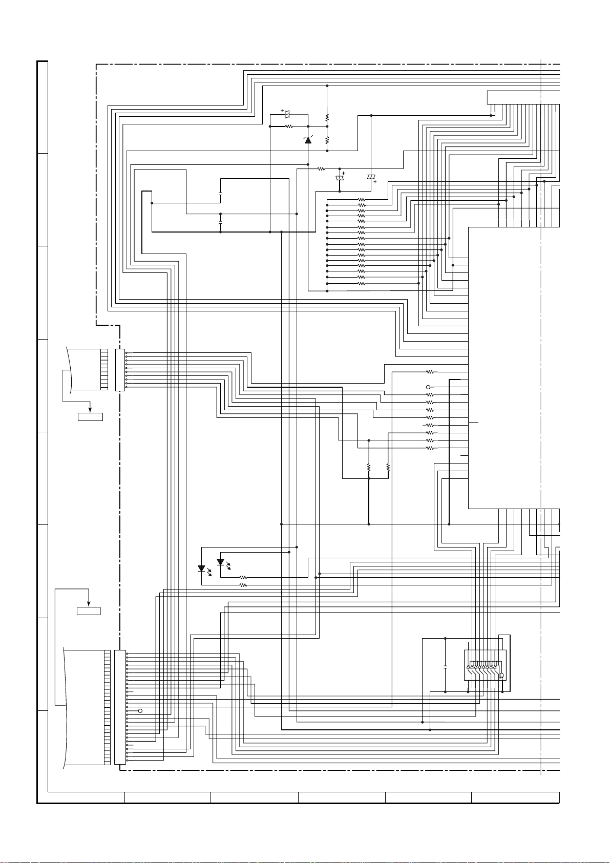
• NOTES ON SCHEMATIC DIAGRAM can be found on page 9.
1
23456
Figure 20 SCHEMATIC DIAGRAM (7/17)
– 20 –
Page 21

47 1K
48 1K
815
.1
C916
0.022
B
R794
100
+B
R989 1K
R990 1K
81
82
83
84
85
86
87
88
89
90
91
92
93
94
95
96
97
98
99
100
+B
R950
10K
R927 10K
R931 10K
R929 1K
R932 1K
R930 1K
R951 1K
R937 1K
P17
P16
P15
P14
P13
P12
P11
P10
P07
P06
P05
P04
P03
P02
P01
PO0
AN7
AN6
AN5
AN4
SYSTEM MICROCOMPUTER
AN3
AN2
AN1
AVSS
AN0
VREF
AVCC
P97
P96
P95
P94
P93
P92
P91
P90
R902 1K
R903 1K
R904 1K
R960
220K
R912
BYTE
10K
123 4 5 6 7 8 9
R901 1K
R949 1K
P27
P26
P25
P24
P23
P22
P21
P20
IC710
IX0489AW
CNVSS
P87
P86
RESETB
XOUT
VSS1
XIN
VCC1
10111213141516171819
C912
47P
(CH)
R905
22
R906
8.38 MHz
820
C902
15P
(CH)
R928
10K
+B
P34
P33
P32
P31
P30
VCC2
VSS2
P85
P84
P83
P82
P81
P80
P77
2021 22 23 24 25 26 2728 29 30
R909 1K
R962 1K
R963 1K
R908 10K
C901
0.22
R907
10K
+B
X901
C905
C903
18P
15P
(CH)
(CH)
P40
P37
P36
P35
P76
P75
P74
P73
R964 1K
515253545556575859606162636465666768697071727374757677787980
P43
P42
P41
P72
P71
P70
R965 1K
50
P44
49
P45
48
P46
47
P47
46
P50
45
P51
44
P52
43
P53
42
P54
41
P55
40
P56
39
P57
38
P60
37
P61
36
P62
35
P63
34
P64
33
P65
32
P66
31
P67
R915
1K
R911
1K
R910
10K
R966 1K
R967 1K
C906
+3.3V
R924 1K
R923 1K
R922 10K
R925 1K
R921 10K
R920 1K
R919 1K
R918 1K
R917 1K
R916 1K
R934 1K
R935 1K
R987 220
R936 220
R913
10K
0.022
R914
10K
HT-CN300
39
F_RLY
[3]
40
C_RLY
[3]
41
S_RLY
[3]
W_RLY
[3]
42
+B
W_SP_RLY
42
7
DSP_INTREQ
8
DSP_ABOUT
9
ROM
DSP_UC17
10
11
DSP_UC16
DSP_UC15
12
13
DSP_RESET
14
DSP_CS
DSP_SCCLK
15
16
DSP_SCDOUT
DSP_SCDIN
1
2
3
4
5
6
7
8
9
CNP708
1
2
3
4
5
6
7
8
9
10
11
12
13
14
17
F_BUSY
F_SCLK
F_RXD
F_TXD
RESET
F_VCC
GND
VCC
VCC
18
19
SDA
SCL
R766
10K
47K
47K
R957
47K
R956
ATT20DB
[3]
FANCNT
+B
+B
[3]
47K
R958
R959
+B
44
45
[1]
[1]
1
20DB_ATT
RLY_F_SP
FAN_CNT
RLY_C_SP
CCB_CE0
RLY_S_SP
CCB_CLK
RLY_W_SP
DATA
THRMO
CCB_DO
PROTECT
DGND
POWER_LEVEL
14
[3]
[1]
[1]
[1]
[1]
[1]
[1]
[1]
[1]
[1]
[1]
[1]
FW8
46
POWLEV
47
PROTECT
48
THERMO
FM SIGNAL
7
8 9 10 11 12
CNP712
1
1
2
3
4
5
6
7
8
8
TUN_L
49
50
AGND_A
51
TUN_R
[3]
[3]
[3]
FW9
CCB_CE0
CCB_CLK
DATA
CCB_DO
AGND
TUNER_R
AGND
TUNER_L
[3]
[1,3]
[3]
CON301
TUNER PWB
P27 12-H
CON301
TO
DISPLAY PWB
P17 12-C
TO
Figure 21 SCHEMATIC DIAGRAM (8/17)
– 21 –
Page 22

HT-CN300
P
9
4
K
[1]
[1]
[1]
[1]
[1]
[1]
A
DSP_SWOUT
DSP_COUT
DSP_SLOUT
DSP_SROUT
DSP_FLOUT
DSP_FROUT
232425262827
DSP PWB-A1 (3/3)
R801
R802
C802
27K
C804
0.015
R804
10/16
220
FM SIGNAL
C801
R803
10/16
220
27K
C803
0.015
B
GND
R846
R844
C847
100P
(CH)
560
SR_OUT
1K
GND
C_OUT
SW_OUT
IC716
NJM4580M
OPE AMP.
C
R834
C826
(CH)
R840
1K
C718
0.022
47P
5
VPP
IN2P
IN1P
6
IN2N
7
IN1N
OUT2
8
OUT1
VDD
C829
0.022
100
R816
100K
R843
100K
R835
1K
C827
4
100P
3
(CH)
2
1
560
R841
D
–B
AGND
C894
10/16
R738
10
C950
100/16
R877
3.9K
R875
220
SORROUND R-CH
CENTER-CH
LSELO
LTRE
LBASS
LOUT
1K
R861
LIN
VSB
C879
L1R1
L2
L3
L4
CE
DI
1/50
12
11
10
9
8
7
6
5
4
3
2
1
R862
1K
C_OUT
IC712
LC75341M
AUDIO
PROCESSOR
C939
1/50
C880
0.0027
C881
0.1
C882
0.1
C884 100P(CH)
C885 100P(CH)
C886 100P(CH)
1K
R943
R864
3.9K
R874
220
C883
10/16
SOBWOOFER-CH
C866
1/50
E
C867
0.0027
R865
3.9K
C870
10/16
F
330
C952
R739
100/16
R873
220
C951
0.022
C871
10/16
C869
0.1
C816
0.022
13
SW_OUT
14
R2
15
R3
C929
16
R4
1/50
17
RSEL
18
RIN
19
RTRE
C868
20
RBASS
0.1
21
ROUT
22
VREF
23
VDD
24
CLK
+B
C949
0.022
C891
0.0027
C895
10/16
C893
C817
0.022
+B+B
C961
1/50
C890
1/50
C892
0.1
0.1
+B
R805
C805
10/16
27K
220
R807
C807
0.015
SL_OUT
NJM4580M
OPE AMP.
5
6
IN2N
7
OUT2
8
VDD
C850
0.022
R854
100K
SR_OUT
13
14
R2
15
R3
16
R4
17
RSEL
18
RIN
19
RTRE
20
RBASS
21
ROUT
22
VREF
23
VDD
24
CLK
R806
27K
C808
0.015
IC711
C853
0.022
VPPIN2P
IN1P
IN1N
OUT1
R849
100K
AGND
SL_OUT
IC713
R878
LSELO
LTRE
LBASS
LOUT
LC75341M
1K
C809
10/16
C806
10/16
220
220
R811
R808
R850
1K
4
C851
3
100P
2
(CH)
1
560
R863
–B
SORROUND L-CH
C962
1/50
12
L1R1
11
L2
10
L3
PROCESSOR
C899
9
L4
1/50
8
7
LIN
6
C900
5
0.1
4
VSB
3
2
CE
1
DI
1K
1K
R879
R880
R809
R810
27K
27K
C811
C812
0.015
0.015
L_OUT
R856
1K
C837
100P(CH)
R822
560
IC713
LC75341M
AUDIO
C904
0.0027
R867
3.9K
R872
C921
0.1
C923 100P(CH)
C924 100P(CH)
C925 100P(CH)
C810
10/16
220
R812
C854
0.022
5
VP
IN2P
6
IN1P
IN2N
7
IN1N
OUT2
8
OUT1
VDD
C843
0.022
R82
100
R823
100K
+B
L_OUT
R_OUT
AGND
+B
–B
C932
C922
10/16
10/16
220
R78
R729
330
330
G
[2]
[2]
[2]
[2]
[2]
CLK
DATA
CCB_CE2
CCB_CE1
CCB_CE0
35
34
33
37
36
H
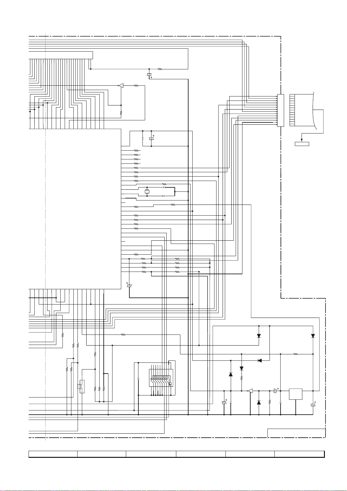
• NOTES ON SCHEMATIC DIAGRAM can be found on page 9.
1
23456
Figure 22 SCHEMATIC DIAGRAM (9/17)
– 22 –
Page 23

[1]
DSP_FROUT
23
C810
R812
56
K
)
+B
+B
3
41M
IO
SOR
867
.9K
872
220
P(CH)
P(CH)
P(CH)
10/16
220
5
6
7
8
R823
100K
–B
R729
330
IN2N
OUT2
VDD
C843
0.022
C922
10/16
R_OUT
AGND
C854
0.022
VPPIN2P
IN1P
IN1N
OUT1
R824
100K
L_OUT
C932
10/16
R789
330
R859
1K
4
3
2
1
–B
FRONT R-CH
C917 1/50
0.0027
R938
220
C948
C839
100P
(CH)
R825
560
NJM4580M
OPE AMP.
1K
R771
C865 1/50
R793
C930
R894
3.9K
C934
0.1
C935
10/16
C818
0.022
C947
0.022
100/16
C825
270P(CH)
C759
270P(CH)
C838
270P(CH)
C742
270P(CH)
C823
270P(CH)
C824
270P(CH)
IC715
PROCESSOR
1K
1K
R769
R770
1K
C931
0.1
+B
AGND
20
18K
R975
R978
33K
IC720
LC75341M
AUDIO
R768
1K
13
AUX IN
14
R2
VCR2 IN
15
R3
VCR1 IN
16
R4
TUNER IN
17
RSEL
18
RIN
19
RTRE
20
RBASS
21
ROUT
22
VREF
23
VDD
24
CLK
C956
C957
LSELO
LTRE
LBASS
LOUT
1K
R881
[1]
C953
10/16
(CH)
150P
100P(CH)
R977
12K
R775
1K
L1R1
L2
L3
L4
LIN
VSB
CE
DI
R973
220
12
11
10
9
8
7
6
5
4
3
2
1
R882
–B
1K
[1]
DSP_AUDIOIN_L
R971
100K
1
OUT1
2
IN1N
3
IN1P
4 5
VPP IN2P
C960
0.022
C964
560P
(CH)
1K
1K
1K
R774
R773
R772
R820
C940
1K
0.0027
C941
0.1
C942
0.1
C944 100P(CH)
C945 100P(CH)
C946 100P(CH)
1K
R883
R972
100K
C955
0.022
VDD
OUT2
IN2N
C965
560P(CH)
DSP_L_IN
C878 1/50
R884
R887
220
[1]
2122
8
7
6
DSP_R_IN
FRONT L-CH
C918 1/50
3.9K
UNSW5V
[1,2]
[1,2]
[1,2]
[1,2]
DSP_AUDIOIN_R
[2]
[2]
[2]
PROTECT
[2,3]
C954
10/16
R974
220
+B
(CH)
150P
C958
(CH)
100P
C959
R982
12K
R979
33K
VCR1_REC_L
AGND
VCR1_REC_R
C864 1/50
C861 1/50
C873 1/50
C862 1/50
C874 1/50
C863 1/50
C875 1/50
C876 1/50
[2]
L_MUTE
330
R790
C943
10/16
FL_OUT
FR_OUT
2
6
DGND
3.3V
1
SW5V
30
VF2
31
VF1
32
VP
47
18K
R976
NJM4580M
OPE AMP.
AGND_A
[1,2]
+B
38
+B
5
IC718
L731
L732
L733
L734
L735
L736
L737
L738
HT-CN300
+B
R828
R827
R799
+B
C732
0.022
29
+B
1K
1K
1K
Q704
2SD1898
12
3
C720
100/16
–B
TUNER_L
TUNER_R
R814
220
11
13
15
17
19
1
3
5
7
9
C813
0.022
DGND_FL
C814
0.022
49
51
CNP711
FL_PRIOUT
A_GND
FR_PRIOUT
SR_PRIOUT
A_GND
SL_PRIOUT
C_PRIOUT
A_GND
SW_PRIOUT
A_GND
F_RLY
C_RLY
W_RLY
-20DBATT
FAN_CONT
THERMO
PROTECT
POW_LEV
S_RLY
TUN_L
TUN_R
1
3
5
7
9
11
13
15
17
+9V
+B
L901
2.2µH
1
3
3
2
L903
2.2µH
AUX_R
AUX_L
VIDEO2_R
VIDEO2_L
VIDEO1_R
VIDEO1_L
REC_R
REC_L
L_MUTE
2
4
6
8
10
12
14
16
18
1
2
3
4
5
6
7
8
9
10
11
12
-9V
–B
2
C972
220/16
1
[2]
[2]
CNP710
GND_AUDIO
GND_AUDIO
GND_AUDIO
GND_AUDIO
GND_AUDIO
GND_AUDIO
GND_AUDIO
GND_AUDIO
41
42
45
47
CNP713
VF2
VF1
-VP
A_GND1
-9V
UNSW_5V
D_GND_FL
D_GND_DSP
+9V
+3.3V1
+3.3V2
SW_5V
C971
100/16
L741
2
4
6
8
10
12
14
16
S_RLY
W_RLY
FANCNT
PROTECT
[2]
[2]
[2]
[2,3]
A & D
FW10
D
D
D
A
CNS102
A
D
FROM
D
AMP. PWB
D
P24 1 - G
A
D
D
CNP550
TO
AUDIO PWB
P30 1 - C
FW12
CNP122
TO
AMP. PWB
P14 1 - G
SL_OUT
SR_OUT
C_OUT
SW_OUT
7
8 9 10 11 12
46
48
44
40
39
POWLEV
THERMO
ATT20DB
C_RLY
F_RLY
[2]
[2]
[2]
[2]
[2]
Figure 23 SCHEMATIC DIAGRAM (10/17)
– 23 –
Page 24

HT-CN300
U
Y
A
TO
AMP. PWB
P15 12 - C
FANGND
M_12VA
PGND_A
AMP. PWB-B3 (2/2)
1
FANB
2
+B
4
5
PGND
6
-B
7
8
+B
-B
B
C
M_12VA
+B
+B
+9V
+B
+B
D
E
F
G
CNP302
TO
TUNER PWB
P27 11 - F
CNP713
TO
DSP PWB
P23 12 - B
CNP431
TO
VIDEO PWB
P28 1 - D
CNS104
CNS102
CNS103
+9V
A_GTUN
D_GTUN
VF2
VF1
-VP
A_GND
-9V
UN_SW_5V
D_GND
D_GND
+9V
+3.3V
+3.3V
SW_5V
-5V
VIDEO_GND
SW_5V
ASSIST
UN_SW_5V
UN_SW_GND
BI104
1
2
3
BI102
1
2
3
4
5
6
7
8
9
10
11
12
BI103
1
2
3
4
5
6
C129
R116
22K
Z113
DZ5.6BSB
B
E
C
Q113
KTA1274
-9V
-5V
0.022
–B
-5V
–B
+B
IC103
SW_5V
+B
+B
+B
+B
+B
+B
+B
+B
VF2
VF1
+3.3V
SW_5V
VOLTAGE REG
+B
C127
47/10
+B
+B
–B
R139 10
BA033T
3
INOUT
GND
2
H
• NOTES ON SCHEMATIC DIAGRAM can be found on page 9.
1
23456
Figure 24 SCHEMATIC DIAGRAM (11/17)
– 24 –
Page 25

+B
-B
Z113
DZ5.6BSB
B
E
C
Q113
KTA1274 Y
C119
22/50
R115
680
C116
47/16
HT-CN300
D101
TS6B04GM
4
+B
6800/16
2200/16
C113
C114
2
3
C101
0.047
(ML)
C102
0.047
(ML)
+B
D111
1N4004S
+B
D112
1N4004S
D113
1N4004S
D114
1N4004S
1
C141
6800/50
C142
6800/50
-B
R155
3.3
+B
Q150
KTC2026
+B
312
R150
330
C130
0.022
DZ10BSB
DZ10BSB
R114
22K
Z150
Z112
B
E
Q112
KTA1274 Y
C
C117
470/16
C118
22/50
R113
1K
8A/125V
C111
0.047
(ML)
C112
0.047
(ML)
F101
8A/125V
F102
F112
1.25A/125V
F111
1.25A/125V
CNP101
1
2
3
S1
S1
GND
CNS101
FROM
MAIN
TRANSFORMER
P29 12 - G
+B
IC103
BA033T
+B
LTAGE REGULATOR
1
3
INOUT
GND
2
C126
0.022
C133
0.022
C125
47/10
Z131
DZ27BSB
KTA1274 Y
E
Q132
CNP107
1
S5
2
S5
3
S4
4
D121
C131
220/63
1N4004S
D122
1N4004S
D123
1N4004S
D124
1N4004S
D131
1N4004S
+B
C123
C124
0.022
C132
0.022
R131
B
C
1K
2200/16
F121
800mA/125V
C122
0.047
(ML)
C121
0.047
(ML)
S4
S3
S3
S2
S2
S2
5
6
7
8
9
CNS107
FROM
MAIN
TRANSFORMER
P29 12 - F
7
8 9 10 11 12
Figure 25 SCHEMATIC DIAGRAM (12/17)
– 25 –
Page 26

HT-CN300
AM MIX OUT AM OSC IN
2
2
1
3
0
1
N
C387 0022
A
CHASSIS
GND
B
AM LOOP
ANTENNA
FM
ANTENNA
C
TUNER PWB-B2
CNP301
1
1
2
2
3
3
C338 0.001
D302 DS1SS133
D301 DS1SS133
FM SIGNAL
AM SIGNAL
AM TRACKING
AM ANTENNA
C323
0.022
AM BAND
COVERAGE fL
T306
AM OSC.
C337
0.022
T302
C339
100P
C335
330P
C330
12P(UJ)
C334
15P(UJ)
VD301
SVC348S
R323
68K
CF302
C331
0.047
C332
0.022
1
C342
0.022
VR351
10K(B)
FM MUTE
LEVEL
R336
10K
3
2
AGND7
R358
8.2K
L353
1mH
C343
33P
R351
5.6K
C351 0.022
C362
3.3/50
C350 0.047
C352 10/50
T351
AM IF
C361
0.022
2324
AM_OSC_OUT
FM_IF_IN
1
C397
0.022
R381
10K
C381
12P(CH)
X352
4.5 MHz
C382
15P(CH)
R374 1K
C394
47/25
C392
0.001
C393
R380
1/50
X_OUT
X_IN
1 2 3 4 5
1
R373 1K
R372 1K
C380
10/16
1.5K
R379
VSS
AOUT
IC3
LC72
PLL(TU
NC1CEDI
DS1SS
R371
4.7K
3
2
Q371
KTA1266 GR
2.2K
1819202122
AIN
CL PD
D35
R
5.
D
C347
0.022
L342
2.2µH
TP301
+B
+B
+B
C345 0.022
C390 0.001
E
D305
DS1SS133
D306
F
D303
DS1SS133
D304
DS1SS133
C301
0.001
CHASSIS
GND
DS1SS133
C321 100/16
R369
47
ANT
GND1
GND2
FE301
FM FRONT END
VCC
C346 0.022
+B
C341
0.022
12345678
VT
GND0
F_OUT
IF_OUT
VDD
R382
150
+B
C310 100P
C311 100P
C312 100P
G
C389
0.001
H
• NOTES ON SCHEMATIC DIAGRAM can be found on page 9.
1
23456
Figure 26 SCHEMATIC DIAGRAM (13/17)
– 26 –
Page 27

HT-CN300
R3
3
1K
C362
.3/50
C350 0.047
C363 0.022
FM_AFC
AM_RF_IN
REG
AM_IF_IN
R352 1K
3
CF352
C364 4.7/50
VSM
FM/AM_OUT
AM_LOW_CUT
GNDSDSTEREO
R353
C353
0.022
C354
C361
0.022
AM_OSC_IN
AM_OSC_OUT
FM_IF_IN
AM_MIX_OUT
1 2 3 4 5 6 7 8 9 10 11 12
1
T351
2
AM IF
MPX_VCO
FM_DET
270
CF351
0.022
C366 0.001
C365 0.022
131415161718192021222324
MPX_IN
L-CH_OUT
R-CH_OUT
VCC
IF_OUT
PHASE
C399
0.022
C377
0.047
R350
2.7K
C367
1/50
MO/ST
LA1832S
FM IF DET./
FM MPX./
PHASE(FM/AM)
C357
2.2/50
C398
100/10
IC303
AM IF
C358
1/50
C356
0.001
C355
22P
R355
X351
456 kHz
3.3K
R359
1.8K
C370
1/50
TP302
R354
3.9K
R357
470K
R356
1K
C368
1/50
C376
0.022
C374
0.033
C373
0.033
C372
1/50
C371
1/50
R362
L352
100µH
1.8K
R361
1.8K
R363
2.7K
R364
2.7K
C396
100/10
C394
47/25
7
C380
10/16
C392
0.001
C393
R380
1/50
1.5K
X_OUT
PLL(TUNER)
X_IN
1 2 3 4 5 6 7 8 9 10 11
3
1
R372 1K
KTA1266 GR
C387 0.022
2.2K
R379
PD
AIN
VSS
AOUT
IC302
LC72131
NC1CEDICLDOFMMW
D352
DS1SS133
R384
5.6K
R371
4.7K
2
Q371
R399
10K
R389
3.9K
R393
R377
1K
47K
L351
100µH
VDD
AM_IN
FM_IN
R385
5.6K
C391
47/25
C385
0.01
NC2
MUTE
IO2
MO/ST
R383
5.6K
1213141516171819202122
ST_IND IF_IN
+B
C386
330P
3
R376
1K
2
1
+B
82K
R378
Q360
KTA1266 GR
R395
47K
R360
4.7K
R392
220
+B
+B
+B
C395
0.022
Z351
DZ5.1BSB
+B
R391
220
+B
CNP302
3
+B
+B
+B+B
2
+9V
CNS104
1
FROM
AMP. PWB
P24 1 - E
CON301
1
8
FW9
TUNER_L
AGND
TUNER_R
AGND
CCB_DO
DATA
CCB_CLK
CCB_CE0
1
2
3
4
5
6
7
8
CNP712
TO
7
8 9 10 11 12
DSP PWB
P21 12 - G
Figure 27 SCHEMATIC DIAGRAM (14/17)
– 27 –
Page 28

HT-CN300
4
4
/
6
5
4
3
C
1
VIDEO PWB-B7
VIDEO SIGNAL
A
R483
1K
1K
R480
R481
1K
R482
FW11
OSD_CS1
V_MUTE
V_SW2
B
DATA
V_SW1
V_REC_MUTE
FUNC_DVD
D_GND
AC_RLY
CNP704
DSP PWB
P20 5 - H
CLK
TO
1
2
3
4
5
6
7
8
9
10
11
11
–B
–B
+B
L452
100µH
+B
C452
100/16
C455
0.022
CNP430
1
L451
100µH
L450
100µH
C451
100/16
C450
100/16
C432 24P(CH)
R435
120
R437
1.5K
+B
TC432
20P
L432
5.6µH
C433
24P(CH)
R434
R436
6.8K
C436 0.0068
C476
1/50
C430
0.022
R428
2.2K
R427
2.7K
+B
C422
0.022
C
C437
20P(CH)
C438
20P(CH)
CNP431
–B
1
-5V
2
GND_VIDEO
3
SW_5V
CNS103
FROM
AMP. PWB
P24 1 - G
D
4
ASSIST
5
UN_SW_5V
6
UN_SW_GND
+B
+B
R408
R409
R410
C408
100P
E
1K
1K
1K
C416
0.022
C409
100P
KRC107 M
B
X437
14.32 MHz
C417
4.7/50
Q416
C
E
C407
100P
IC401
LC74763
OSD.
VSS1
1
X-IN1
2
X-OUT1
3
HSYNC_OUT
4
X-IN2
5
X-OUT2
6
VSYNC_OUT
7
CS
8
SIN
9
SCLK
10
SECAM
11
525/625
12
NTSC/PAL
13
3.58/4.43
14
RST CV_OUT
15 16
VDD1
SYNC_DET
VCO_OUT
VCO_IN
AMP_OUT
AMP_IN
PD_OUT
VSS2
SEPC
SYNC_IN
CV_CR
CV_IN
VDD2
FC
+B
30
29
28
27
26
25
24
23
22
21
20
19
18
17
1K
C483
0.001
C434 0.022
1K
C435
1/50
(N.P.)
R477
220
C477
0.0012
+B
C427
4.7/50
C421
33/16
C481
C482
0.001
0.001
VIDEO DRIVER
NCIN
4
OUT
GND
5
STBY
VCC
6
C480
0.001
+B
C454
0.022
C453
0.022
+B
+B
IC404
TK15406M
C420
470/6.3
3
2
1
R4
–B
C463
33/16
R463
R466
1K
Z460
DZ6.2BSB
7
C
33
–B
13
12 11
14
SW2
VEE
VIN1
VIN3
SW1
VIN2
MUTE2 MUTE1
4
321
C
3
R
7
75
R420
75
F
AC POWER
SUPPRY CORD
AC 120 V, 60 Hz
F511
4A/125V
L511
AC LINE FILTER
TRANSFORMER
G
H
• NOTES ON SCHEMATIC DIAGRAM can be found on page 9.
1
23456
Figure 28 SCHEMATIC DIAGRAM (15/17)
C511
0.0047
T501
SUB
– 28 –
C521
0.047
(ML)
RY511
D521
DS1SS133
D522 1N4004S
D523 1N4004S
D524 1N4004S
D525 1N4004S
IC501
KA7805AP
VOLTAGE
REGULATOR
C522
470/35
GND
OUTIN
2
31
D526
DS1SS133
+B
C523
1000/6.3
C
B
E
Q521
KTC3198 GR
R522
47K
R523
100
Page 29

R461
C461
33/16
HT-CN300
C412
47P
C415
47P
C423
100P
C425
L420
30P
2.2µH
75
C424
220P
TV
DVD-IN
C403
0.001
J420
TV MONITOR OUT
J430
DVD IN
66
K
Z460
6.2BSB
0
–B
C463
33/16
R463
75
13
14
VEE
VIN3
12 11 10 9 8
SW2
VIN1
MUTE1
SW1
VIN2
MUTE2
C462
33/16
R462
75
C460
10/16
VOUT1
VOUT2
NC
GND2
GND1 VDD
7654321
+B
C459
0.022
DS1SS133
IC402
NJM2279D
VIDEO
SWITCH
C465
R465
470/6.3
D460
R460
15K
75
C464
100/16
C497
0.022
C496
0.022
R495
75
C495
33/16
R493
75
VIDEO SWITCH
VEE
VIN3
1
SW2
SW1
2
VIN2
VIN1
3
MUTE2
MUTE1
4
VOUT2
VOUT1
5
GND2
6
7 8
NC
GND1 VDD
IC405
NJM2279D
+B
–B
14
C494
33/16
R492
R494
75
75
VIDEO2-IN
VIDEO1-IN
VIDEO-1 REC
C466
47P
D402
DS1SS133
D401
CHASSIS
GND1
CHASSIS
GND1
CHASSIS
GND2
DS1SS133
CHASSIS
GND1
VIDEO IN/OUT
D403
DS1SS133
D404
DS1SS133
D_GND
J401
VTR2 IN
VTR1 IN
VTR1 OUT
0.001
CHASSIS
GND3
C406
13
12
11
10
9
Q521
KTC3198 GR
B
R522
47K
R523
100
+B
T100
MAIN TRANSFORMER
CNS107
CNP510
1
2
D527
R527
1N4004S
3.3
+B
C525
100/16
7
8 9 10 11 12
CNS510
CNP107
TO
AMP. PWB
P25 12 - E
CNS101
CNP101
T.F.
TO
AMP. PWB
P25 12 - B
Figure 29 SCHEMATIC DIAGRAM (16/17)
– 29 –
Page 30
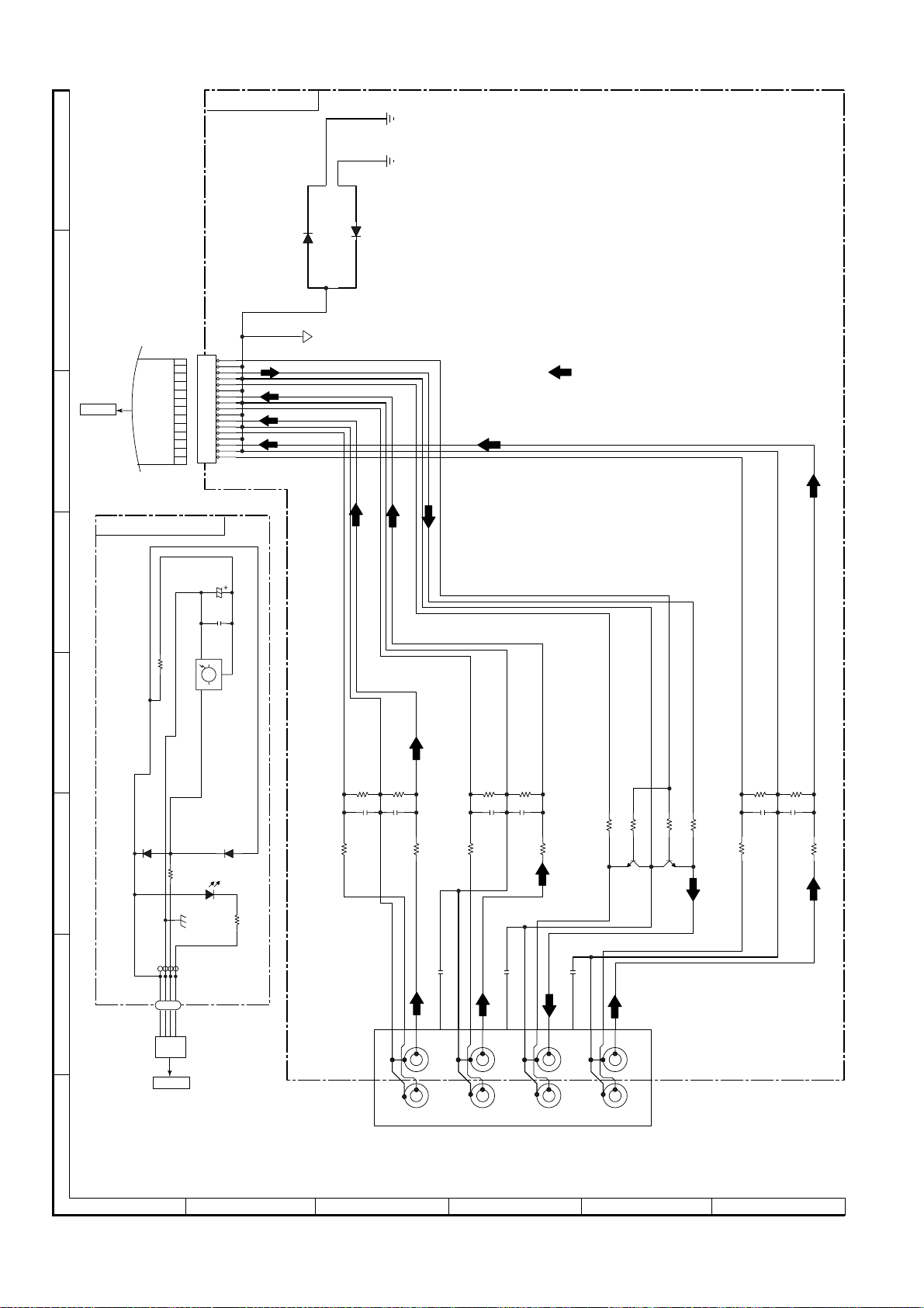
HT-CN300
AUDIO PWB-B4
A
D596
DS1SS133
D597
DS1SS133
CHASSIS
GND1
CHASSIS
GND2
B
FW10
L_MUTE
AGND
REC_L
TO
DSP PWB
P23 12 - E
CNP710
C
AGND
REC_R
AGND
VIDEO1_L
AGND
VIDEO1_R
AGND
VIDEO2_L
AGND
VIDEO2_R
AGND
AUX_L
AGND
AUX_R
CNP550
1
1
2
3
4
5
6
7
8
9
10
11
12
13
14
15
16
17
17
AGND
FM SIGNAL
AUX
SENSOR PWB-A2
VIDEO2
VIDEO1
VIDEO1-REC
+B
D
100
R10
E
C11
47/16
C10
0.022
3
IC10
2
1
GP1UM261
REMOTE SENSOR
+B
+B
R13
1K
1234
GND
D11
KDS160
+B
LED12
333ID231
RED
R12
680
D10
KDS160
F
+B
+B
+5V
BI10
G
CNS10
R561
3.9K
J550
AUDIO IN/OUT
R563
39K
C561
47P
R564
39K
C562
47P
L-CH
R562
3.9K
C563
0.001
R571
3.9K
L-CH
R573
39K
C571
47P
C573
0.001
R574
39K
C572
47P
L-CH
R572
3.9K
C583
0.001
L-CH
R581
2.7K
R583
E
3.3K
B
Q581
3.3K
R584
B
C
C
Q582
KTC3198 GR
2.7K
R582
E
KTC3198 GR
R551
3.9K
R553
39K
C551
47P
R554
39K
C552
47P
R552
3.9K
CNP702
TO
DSP PWB
P20 1 - B
R-CH
AUDIO2 IN
R-CH
AUDIO1 IN
R-CH
AUDIO OUT
R-CH
AUDIO/AUX IN
H
1
23456
Figure 30 SCHEMATIC DIAGRAM (17/17)
– 30 –
Page 31

IC201
PIN
VOLTAGE
NO.
10 V
29.3 V
2
3
0 V
0 V
4
0 V
5
3.6 V
6
0 V
7
0 V
8
0 V
9
10 0 V
11 3.6 V
12 0 V
13 0 V
14 0 V
15 29.3 V
IC202
PIN
VOLTAGE
NO.
10 V
29.3 V
2
3
0 V
29.3 V
4
0 V
5
3.6 V
6
0 V
7
0 V
8
0 V
9
10 0 V
11 3.6 V
12 0 V
13 0 V
14 0 V
15 29.3 V
IC203
PIN
VOLTAGE
NO.
10 V
29.3 V
2
3
0 V
29.3 V
4
0 V
5
3.6 V
6
0 V
7
0 V
8
0 V
9
10 0 V
11 3.6 V
12 0 V
13 0 V
14 0 V
15 29.3 V
IC302
PIN
VOLTAGE
NO.
1 2.5 V
0 V
2
3
0 V
1.7 V
4
4.1 V
5
5.1 V
6
0 V
7
3.9 V
8
0 V
9
10 4 V
11 5.1 V
12 2.5 V
13 0 V
14 0 V
15 0 V
16 2.5 V
17 5.2 V
18 0.8 V
19 0.8 V
20 2.9 V
21 0 V
22 2.5 V
IC303
PIN
VOLTAGE
NO.
1 2.2 V
5 V
2
3
2.2 V
2.2 V
4
0 V
5
0 V
6
5.1 V
7
3 V
8
5 V
9
10 0 V
11 3.9 V
12 3.9 V
13 4 V
14 1.3 V
15 1.3 V
16 2.2 V
17 2.4 V
18 2.7 V
19 0 V
20 2.3 V
21 2.3 V
22 2.3 V
23 5 V
24 3.5 V
IC401
PIN
VOLTAGE
NO.
10 V
2.5 V
2
3
2.6 V
4.6 V
4
4.6 V
5
5 V
6
5 V
7
2.5 V
8
0.4 V
9
10 4.4 V
11 0 V
12 0 V
13 0 V
14 0 V
15 5 V
16 0.8 V
17 4.8 V
18 0.8 V
19 0.5 V
20 2 V
21 2 V
22 0 V
23 2.5 V
24 2.5 V
25 2.6 V
2.6 V
26
27
2.5 V
2.5 V
28
0.4 V
29
5 V
30
IC402
PIN
VOLTAGE
NO.
10 V
0.01 V
2
3
0.03 V
0.01 V
4
0.05 V
5
0 V
6
0 V
7
4.8 V
8
0 V
9
10 0 V
11 4.8 V
12 0 V
13 4.5 V
14 4.8 V
IC404
PIN
VOLTAGE
NO.
1 1.4 V
2.4 V
2
3
2.4 V
2.4 V
4
0 V
5
4.8 V
6
IC405
PIN
VOLTAGE
NO.
10 V
0 V
2
3
0.03 V
0.01 V
4
0.05 V
5
0 V
6
0 V
7
4.8 V
8
0 V
9
10 0 V
11 0 V
12 0 V
13 0 V
14 4.8 V
IC603
PIN
VOLTAGE
NO.
10 V
0 V
2
3
3 V
1.6 V
4
0 V
5
0 V
6
0 V
7
0 V
8
0 V
9
10 0 V
11 0 V
12 0 V
13 0 V
14 0 V
15 0 V
16 4.3 V
17 4.6 V
18 0 V
19 0 V
20 5 V
IC604
PIN
VOLTAGE
NO.
10 V
3.4 V
2
3
3.4 V
0 V
4
3.4 V
5
0 V
6
0 V
7
3.4 V
8
2.2 V
9
10 0 V
11 0 V
12 5 V
13 0 V
14 0 V
15 5 V
16 0 V
17 5 V
18 5 V
19 0 V
20 5 V
IC718
PIN
VOLTAGE
NO.
10 V
0 V
2
3
0 V
9.3 V
4
0 V
5
0 V
6
0 V
7
8.4 V
8
IC701
PIN
VOLTAGE
NO.
10 V
3.3 V
2
3
3.3 V
3.3 V
4
3.3 V
5
3.3 V
6
3.3 V
7
3.3 V
8
3.3 V
9
10 0 V
11 2.4 V
12 3.3 V
13 3.3 V
14 3.3 V
15 3.3 V
16 3.3 V
17 3.3 V
18 3.3 V
19 3.3 V
20 3.3 V
IC702
PIN
VOLTAGE
NO.
10 V
2.4 V
2
3
2.4 V
2.4 V
4
2.4 V
5
2.4 V
6
2.4 V
7
2.4 V
8
2.4 V
9
10 0 V
11 2.4 V
12 3.3 V
13 3.3 V
14 3.3 V
15 3.3 V
16 3.3 V
17 3.3 V
18 3.3 V
19 3.3 V
20 3.3 V
IC703
PIN
VOLTAGE
NO.
1 3.3 V
3.3 V
2
3
3.3 V
3.3 V
4
3.3 V
5
0 V
6
3.3 V
7
3.3 V
8
3.3 V
9
10 0 V
11 0 V
12 3.3 V
13 3.3 V
14 3.3 V
15 3.3 V
16 3.3 V
17 3.3 V
18 3.3 V
19 3.3 V
20 3.3 V
21 2.4 V
22 2.4 V
23 2.4 V
24 0 V
25 2.4 V
2.4 V
26
27
2.4 V
2.4 V
28
2.4 V
29
3.4 V
30
3.3 V
31
2.4 V
32
VOLTAGE
IC706
PIN
VOLTAGE
NO.
1 2.4 V
0 V
2
3
1.1 V
0 V
4
2.4 V
5
0 V
6
0 V
7
0 V
8
2.4 V
9
10 2.4 V
11 2.4 V
12 2.4 V
13 0 V
14 2.4 V
15 2.4 V
16 2.4 V
17 2.4 V
18 2.4 V
19 2.4 V
20 2.4 V
21 2.4 V
22 1.2 V
23 2.4 V
24 0 V
25 1.2 V
1.6 V
26
27
1.2 V
1.6 V
28
1.6 V
29
2 V
30
0 V
31
1.9 V
32
1.2 V
33
34 2.5 V
35 0 V
36 3.2 V
37 2.4 V
38 2.4 V
39 0.9 V
40 0.9 V
41 0.9 V
42 1.6 V
43 1.6 V
44 0 V
IC704
PIN
VOLTAGE
NO.
10 V
0 V
2
3
2.4 V
3.3 V
4
0 V
5
0 V
6
0 V
7
3.3 V
8
2.3 V
9
10 2.4 V
11 3.4 V
12 2.4 V
13 3.4 V
14 3.3 V
IC705
PIN
VOLTAGE
NO.
1 3.3 V
3.3 V
2
3
2.5 V
0 V
4
0 V
5
IC707
PIN
VOLTAGE
NO.
1 1.2 V
1.6 V
2
3
0 V
0 V
4
3.3 V
5
1.5 V
6
1.5 V
7
3.3 V
8
PIN
NO.
PIN
NO.
PIN
NO.
PIN
NO.
IC708
VOLTAGE
1 2.5 V
2.2 V
2
3
4.9 V
0 V
4
3.3 V
5
2.5 V
6
1.4 V
7
1.6 V
8
1.6 V
9
10 1.2 V
11 0.9 V
12 0 V
13 0.5 V
14 0 V
15 0 V
16 0 V
17 3.2 V
18 3.2 V
19 0 V
20 0 V
21 0 V
22 4.9 V
23 4.9 V
24 2.4 V
25 0 V
2.4 V
26
27
2.4 V
2.4 V
28
2.4 V
29
2.4 V
30
2.4 V
31
2.4 V
32
2.4 V
33
34 0 V
35 0 V
36 0 V
37 0 V
38 0 V
39 2.4 V
40 0 V
41 2.4 V
42 0 V
43 0 V
44 0 V
IC711
VOLTAGE
10 V
0 V
2
3
0 V
9.3 V
4
0 V
5
0 V
6
0 V
7
8.4 V
8
IC715
VOLTAGE
10 V
0 V
2
3
0 V
9.3 V
4
0 V
5
0 V
6
0 V
7
8.4 V
8
IC716
VOLTAGE
10 V
0 V
2
3
0 V
9.3 V
4
0 V
5
0 V
6
0 V
7
8.4 V
8
PIN
VOLTAGE
NO.
1 1.2 V
3.3 V
2
3
0 V
3.4 V
4
1.4 V
5
0 V
6
1.3 V
7
0 V
8
0 V
9
10 0 V
11 3.4 V
12 3.4 V
13 1.5 V
14 0 V
15 1.4 V
16 3.4 V
17 3.4 V
18 3.3 V
19 0 V
20 3.3 V
21 0 V
22 0 V
23 3.4 V
24 0 V
25
0 V
26
0 V
27
3.4 V
28
0 V
29
3.3 V
30
3.3 V
0 V
31
0 V
32
33
0 V
34
0 V
35
0 V
36
3.3 V
37
0 V
38
3.4 V
39
3.4 V
40
0 V
41
0 V
42
0 V
43
0 V
44
3.4 V
45
0 V
46
3.3 V
47
0 V
48
0 V
49
0 V
50
0 V
IC712
PIN
VOLTAGE
NO.
1 0.4 V
0 V
2
3
0 V
4.2 V
4
4.2 V
5
4.2 V
6
4.2 V
7
4.2 V
8
4.2 V
9
10 4.2 V
11 4.2 V
12 4.2 V
13 4.2 V
14 4.2 V
15 4.2 V
16 4.2 V
17 4.2 V
18 4.2 V
19 4.2 V
20 4.2 V
21 4.2 V
22 4.2 V
23 8.3 V
24 4.4 V
IC102
PIN
VOLTAGE
NO.
1 9.2 V
0 V
2
3
5 V
IC710
PIN
VOLTAGE
NO.
51 3.4 V
3.4 V
52
53
3.4 V
0 V
54
0 V
55
0 V
56
0 V
57
0 V
58
3.4 V
59
60 3.4 V
61 3.3 V
62 3.4 V
63 0 V
64 0 V
65 3.4 V
66 3.4 V
67 3.3 V
68 0 V
69 0 V
70 3.4 V
71 3.4 V
72 3.4 V
73 3.3 V
74 3.3 V
75
0 V
76
3.4 V
77
3.4 V
78
3.4 V
79
3.4 V
80
3.4 V
3.4 V
81
82
3.4 V
83
3.3 V
84
3.4 V
85
3.3 V
86
0 V
87
0 V
88
0 V
89
3.3 V
90
3.3 V
91
3.3 V
92
0.6 V
93
1.6 V
94
0 V
95
3.3 V
96
0 V
97
3.3 V
98
3.3 V
99
3.4 V
100
0 V
IC713
PIN
VOLTAGE
NO.
1 0.4 V
0 V
2
3
0 V
4.2 V
4
4.1 V
5
4.1 V
6
4.1 V
7
4.2 V
8
4.1 V
9
10 4.1 V
11 4.1 V
12 4.1 V
13 4.1 V
14 4.1 V
15 4.1 V
16 4.1 V
17 4.2 V
18 4.1 V
19 4.1 V
20 4.1 V
21 4.2 V
22 4.2 V
23 8.3 V
24 4.9 V
IC103
PIN
VOLTAGE
NO.
15 V
0 V
2
3
3.3 V
PIN
VOLTAGE
NO.
1 4.9 V
2 V
2
3
0 V
2 V
4
0 V
5
0 V
6
4.8 V
7
0 V
8
0 V
9
10 5 V
11 2.3 V
12 2.1 V
13 0 V
14 0 V
15 5.3 V
16 4.9 V
17 4.4 V
18 0.3 V
19 5.2 V
20 0 V
21 0 V
22 4.6 V
23 4.9 V
24 4.3 V
25
0 V
26
0 V
27
3.9 V
28
0 V
29
5 V
30
0 V
0 V
31
32
5 V
33
5 V
34
0 V
35
5 V
36
5.2 V
37
4.8 V
38
4.8 V
39
4.8 V
40
0 V
41
0 V
42
0 V
43
0.3 V
44
6.4 V
45
3.4 V
46
4.9 V
47
5 V
48
5 V
49
0 V
50
2.8 V
IC720
PIN
VOLTAGE
NO.
1 0.4 V
0 V
2
3
0 V
4.2 V
4
4.2 V
5
4.1 V
6
4.1 V
7
4.2 V
8
4.1 V
9
10 4.1 V
11 4.1 V
12 4.1 V
13 4.1 V
14 4.1 V
15 4.1 V
16 4.1 V
17 4.2 V
18 4.1 V
19 4.1 V
20 4.1 V
21 4.2 V
22 4.2 V
23 8.3 V
24 4.9 V
IC501
PIN
VOLTAGE
NO.
1 10.4 V
0.6 V
2
3
5.6 V
HT-CN300
IC901
PIN
VOLTAGE
NO.
51 0 V
52
53
54
55
56
57
58
59
60 0 V
61 0 V
62 0 V
63 4 V
64 0 V
65 4.8 V
66 3.3 V
67 4.9 V
68 4.8 V
69 4.9 V
70 4.9 V
71 26.3 V
72 18 V
73 23.5 V
74 26.3 V
75
76
77
78
79
80
81
82
83
84
85
86
87
88
89
90
91
92
93
94
95
96
97
98
99
100
IC721
PIN
VOLTAGE
NO.
10 V
2
3
4
5
6
7
8
IC722
PIN
VOLTAGE
NO.
10 V
2
3
4
5
6
7
8
9
10 0 V
11 0 V
12 0 V
13 0 V
14 0 V
15 0 V
16 0 V
0 V
5 V
0 V
0 V
2.7 V
4.8 V
2.2 V
4.9 V
15.2 V
20.7 V
23.5 V
15.2 V
0 V
23.5 V
17.9 V
26.3 V
20.7 V
23.5 V
17.9 V
15 V
26.3 V
26.3 V
26.2 V
26.2 V
26.3 V
23.5 V
23.6 V
23.5 V
23.5 V
23.5 V
23.5 V
23.5 V
23.5 V
23.5 V
0 V
0 V
0 V
0.04 V
0 V
0 V
0 V
0 V
0 V
0 V
0 V
0.2 V
0 V
0 V
0.06 V
– 31 –
Page 32

HT-CN300
1
23456789101112
AMP. PWB-B3
CNS104
HW
3
A
2
1
CNP302
TO
TUNER PWB
P34 4 - H
WH
RD
F121
800mA/125V
BRGYGYGYGYGYGYGYGYGYGY
1
RD
1
WH
3
1
WHWHWH
GY
WH
CNS102
12
6
RD
WH
WH
WH
WH
WH
CNP713
TO
DSP PWB
P37 12 - C
CNS103
1
2
3
4
5
6
CNP431
TO
VIDEO PWB
P35 7 - C
B
123
F111
1.25A/125V
C
FROM
MAIN TRANSFORMER
P35 7 - F
F112
1.25A/125V
CNS107
1
234
56789
D
FROM
MAIN TRANSFORMER
P35 8 - F
CNS101
FW12
F101
19
8A/125V
F102
8A/125V
19
18
17
16
15
1
2
3
14
13
12
11
10
9
8
7
6
5
4
3
2
1
3
2
1
15
14
13
12
11
10
9
8
7
6
5
4
3
2
1
E
1
CNP711
TO
DSP PWB
P37 8 - G
8
7
6
5
4
3
2
1
F
15
14
13
12
11
10
9
M200
FAN MOTOR
G
RD
WH
SUBWOOFER UNIT
CNS205
1
2
2
1
1
2
123
1
234567891011
8
7
6
5
4
3
2
1
H
1
23456
Figure 32 WIRING SIDE OF P.W.BOARD (1/6)
– 32 –
Page 33

HT-CN300
AUDIO PWB-B4
AUDIO/AUX IN AUDIO OUT
L-CH R-CH L-CH R-CH
J550
AUDIO IN/OUT
L-CH R-CH
1
3 5 7 9 11 13 15 17
2 4 6 8 10 12 14 16
1
FW10
TERMINAL PWB-B5
CNS204
1
2
3
4
5
6
7
8
1
RD
WH
WH
WH
WH
WH
WH
WH
8
AUDIO1 IN
CNP710
TO
DSP PWB
P37 7-F
AUDIO2 IN
L-CH R-CH
15
14
13
12
11
10
9
8
7
6
5
4
3
2
1
COLOR TABLE
BROWN
BR
RED
RD(R)
ORANGE
OR
YELLOW
YL
GREEN
GR
BLUE
BL
VIOLET
VL
GRAY
GY
WHITE
WH(W)
BLACK
BK
PINK
PK
17
TO
DSP PWB
P37 8-A
CNP702
1
2
34
CNS10
BK
GY
SENSOR PWB-A2
(BOTTOM VIEW)
BK
YL YL
WH WH
RD RD
1
4
C12
R13
1
3
2
SENSOR PWB-A2
(TOP VIEW)
SPEAKER PWB-B6
1
2
3
4
5
6
7
8
9
10
11
+
FRONT
7
8 9 10 11 12
Figure 33 WIRING SIDE OF P.W.BOARD (2/6)
+ + +
SURROUND
L-CH
L-CH
+
CENTER
J201
SPEAKER TERMINAL
– 33 –
FRONT
R-CH
SURROUND
R-CH
Page 34

HT-CN300
DISPLAY PWB-B1
A
123
FW8
14
CNP708
TO
DSP PWB
P37 9 - F
FW6
1
29
B
C
CNP701
TO
DSP PWB
P37 12 - C
D
1
FW7
10
CON703
TO
DSP PWB
P37 12 - E
14
13
12
11
10
9
8
7
6
5
4
3
2
1
100
1
5
95
10
90
15
29
28
27
26
25
24
23
22
21
20
19
18
17
16
15
14
13
12
11
10
9
8
7
6
5
4
3
2
1
20
1
5
15
IC603
11
10
20
1
5
15
IC604
10
11
2468
10
113579
20
30
IC601
25
35
31
40
50
85
75
70
65
60
45
55
51
1
2
4
5
6
7
8
9
10
11
12
13
14
15
16
17
18
19
81
20
21
80
22
23
24
25
26
27
28
29
30
31
32
34
35
POWER
E
TUNER PWB-B2
33221
1 2 3 4 5 6 7 8 9 1011
F
FM
ANTENNA
AM LOOP
G
ANTENNA
3
3
2
2
1
1
H
1
2221201918171615141312
1
1
2
3
4
1
2345678
1 2 3 4 5 6 7 8 9 101112
222120191817161514132324
123
FROM
POWER PWB
CNS104
P32 2 - B
5
6
7
8
FW9
1
8
CNP712
TO
DSP PWB
P37 10 - F
23456
Figure 34 WIRING SIDE OF P.W.BOARD (3/6)
– 34 –
Page 35

VIDEO PWB-B7
HT-CN300
FW11
11
CNP704
TO
DSP PWB
P37 11 - F
CNS103
FROM
AMP. PWB
P32 4 - B
J420
1
11
10
9
8
7
6
5
4
3
2
1
1
1
23456
3
2
1
2 3 4 5 6 7 8 910111213 14 15
201918 17 16252423 22 21302928 27 26
98
IC404
3
46
1413121110
1234567
1
F551
4A/125V
98
1413121110
1234567
TV MOMITOR
J430
DVD IN
VTR2
IN
VTR1
VIDEO
IN
IN/OUT
VTR1
OUT
J401
T501
SUB POWER TRANSFORMER
TO AMP. PWB
P32 2 - C
CNP107
CNS107
1 2 3 4 5 6 7 8 9
BRBRORORYLYLWHBKWH
RD
TO AMP. PWB
P32 2 - D
CNP101
1 2 3
BLRDBK
BK
CNS101
T100
MAIN POWER
TRANSFORMER
L511
AC LINE FILTER
AC POWER
SUPPLY CORD
AC 120 V, 60 Hz
1
2
COLOR TABLE
BROWN
BR
OR
YL
GR
BL
VL
GY
BK
PK
RED
ORANGE
YELLOW
GREEN
BLUE
VIOLET
GRAY
WHITE
BLACK
PINK
RD(R)
WH(W)
12
7
CNS510
8 9 10 11 12
Figure 35 WIRING SIDE OF P.W.BOARD (4/6)
– 35 –
Page 36

HT-CN300
A
DSP PWB-A1(BOTTOM VIEW)
9
5
C925
8
R760
R878
L710
C752
R782
35
20
C749
C924
R741
30
25
12
C904
R867
C900
C921
R872
1
R879
D707
34
22
C923
R880
D701
R755
23
R985
R761
R762
R763
R764
R765
R767
R729
R738
R771
R801
R803
C803
24
C818
D710
D711
R834
5
8
R840
C829
R770
R769
13
15
20
IC720
R881
C947
R802
C718
IC716
R768
10
5
C946
C819
R775
12
R882
R804
C804
4
1
1
C945
R883
R789
R841
R774
R835
R773
C944
C827
R843
R820
C940
R884
C941
C942
R887
C842
R823
R772
D706
R986
33
C754
C732
L715
R793
C930
R894
C931
C934
R938
R974
R972
C955
IC718
R971
R973
R806
R808
C808
R844
C847
R846
R854
R810
R812
C812
C837
C853
5
8
IC711
R856
5
8
C843
R822
IC715
C854
R976
C958
1
R975
R805
C850
C956
C807
R982
C959
R979
C965
8
5
4
C960
C957
C964
R978
R977
R807
R850
4
C851
1
R849
R863
R809
R811
C811
R859
4
C839
1
C841
R824
R825
L733
D709
C760
B
Q701
Q702
D705
R731
Q721
C
C991
R991
R992
R994
R993
C992
R952
R913
D
R940
R942
R944
R794
D704
R954
R990
C815
C916
L714
R945
R946
R947
R948
C739
R951
R989
80
81
100
1
R901
R902
R912
D708
IC701
11
15
5
20
C736
1
5
10
IC703
15
16
R745
C913
R927
R937
C906
R949
R930
R950
R932
R931
R929
85
IC710
90
510152025
R905
R960
R903
C912
R904
R908
R906 C903
R909
C902
C905
X901
C901
R928
R710
R711
R712
IC702
10
11
15
1
20
C738
30
25
20
C725
1
R924
51
50
R922
5560657075
R925
R921
45
R920
R919
40
R918
R917
R916
35
31
R935
30
R987
R936
R915
R963
R965
R966
R962
R964
R967
E
R708
R709
5
14
IC704
R923
R934
R910
R827
R828
R799
R911
R707
1
32
17
C911
D703
D702
C762
IC721
Z705
R705
R706
R740
5
4
C724
1
8
10
R738
R758
R702
R703
R735
R701
6
R704
7
5
10
C707
IC706
15
20 25
17
8
18
R714
R715
R713
7
IC705
R913
R907
R766
R914
Z704
1
2
3
4
5
6
7
8
9
3
2
1
Q703
L704
R926
1
CNP706
R912
C910
C744
R959
R958
R957
R956
L702
5
C728
L901
R733
C705
R716
R746
R730
C726
C731
1
44
R788
L712
Q704
321
C814
L903
R783
R814
C813
R727
C701
R752
R726
R865
C868
C869
L722
C727
R757
35
30
R785
L711
C867
L721
R724
R725
40
39
29
28
C702
R784
R787
IC707
C732
R873
R786
C716
C709
R719
13
24
C816
R720
R723
R722
R721
R728
C761
R717
4
5
C713
IC712
15
20
R861
C951
L713
R718
10
C886
C710
1
8
5
C721
R759
R862
C712
12
1
C885
R955
C711
R943
C884
L708
C733
C880
R864
C882
R874
L709
C881
R895
R751
R750
R749
R748
R747
R753
L707
X701
C820
R984
R983
R815
R851
IC722
16
10
15
5
1
R743
R742
C753
C729
C745
44
1
40
C746
5
IC708
C743
10
15
11
12
R754
R756
C730
IC713
13
15
10
C891
20
R877
C892
C893
R875
24
C817
C949
R60
R739
R790
F
G
H
1
23456
Figure 36 WIRING SIDE OF P.W.BOARD (5/6)
– 36 –
Page 37

HT-CN300
DSP PWB-A1(TOP VIEW)
C703
C822
C876
C917
L734
L735
L737
L732
C962
C874
C875
C878
C810
C806
C805
C961
C943
C809
C802
C759
C879
C801
C825
R816
C948
C953
C750
C757
C935
L741
C863
CNP710
L738
10
12
14
16
L731
2
4
6
8
C824
C862
C864
C823
C918
1
3
5
7
9
11
13
15
17
C861
C873
L732
L736
C954
C866
C835
C865
C932
C751
C756
C734
C748
C899
C742
C922
FROM
SENSOR PWB
P33 10 - C
CNS10
1
234
CNP702
C747
C758
C950
C999
C719
C890
C895
C741
C998
R744
C858
C846
C894
C838
C939
DIGITAL IN
C883
CON707
C708
C720
C784
C781
C971
CNP713
12
11
10
9
8
7
6
5
4
3
2
1
DVD GIGITAL IN
DIG2 JACK
C840
C755
C706
C907
CON703
C821
C735
C740
C729
C908
C909
FROM
DISPLAY PWB
P32 2-D
CNS713
TO
DISPLAY PWB
P34 2 - D
CNP640
FW6
29
28
27
26
25
24
23
22
21
20
19
18
17
16
15
14
13
12
CNP701
11
10
9
8
7
6
5
4
3
2
246810
1
3579
1
FW7
1
29
1
IC709
C844
2 3
C715
C952
C717
C714
C871
C845
C929
C870
C704
C972
1
FW10
1
CNP550
TO
AUDIO PWB
P33 9 - C
7
CNP711
1
3 5 7 9 11 13151719
17
2 4 6 8 1012141618
19
1
FW12
CNP122
TO
AMP. PWB
P32 2 - F
14
CNP708
CNP601
TO
DISPLAY PWB
P34 2 - B
CNP712
24
2468101214
135791113
1
FW8
68
13
57
8
1
FW9
CON301
TO
TUNER PWB
P34 6 - H
CNP704
11357
246810
CNP430
TO
VIDEO PWB
P35 7 - B
9
10
CNP670
TO
DISPLAY PWB
P34 2 - E
10
FW11
8 9 10 11 12
Figure 37 WIRING SIDE OF P.W.BOARD (6/6)
– 37 –
Page 38

HT-CN300
FUNCTION T ABLE OF IC
IC401 VHiLC74763/-1: OSD. (LC74763)
Port NamePin No.
1 VSS GND.
2 XTAL IN 1 Crystal and capacitor connection in the crystal oscillator for an internal sync signal.
3 XTAL OUT 1 Crystal and capacitor connection in the crystal oscillator for an internal sync signal.
4* HSYNC OUT Horizontal sync signal output (AFC).
5* XTAL IN 2 Crystal and capacitor connection in the crystal oscillator for an internal sync signal.
6* XTAL OUT 2 Crystal and capacitor connection in the crystal oscillator for an internal sync signal
7* VSYNC OUT Vertical sync signal output.
8 CS Vertical sync signal output.
9 SIN Serial data input (hysteresis input).
10 SCLK Serial data input clock.
11 SECMA SECAM mode switching at input.
12 526/625 Scan line switching (525/625) at input.
13 NTSC/PAL Color NTSC/PAL switching.
14
15 RET System reset input (active=“L”) (hysteresis input).
16 CV OUT Composite video signal output.
17 VDD 2 Power supply for creating composite video signal levels.
18 CV IN Composite video signal input.
19* CV CR SECAM chrominance signal input.
20 SYNC IN Video signal input in the built-in sync separation circuit.
21* SEPC Bias input in the built-in sync separation circuit.
22 VSS GND.
23 PD OUT AFC control voltage output.
24 AMP IN Filter.
25 AMP OUT Filter.
26 FC AFC control voltage input.
27 VCON IN Coil and capacitor connection in the LC oscillator for VCO.
28 VCO OUT Coil and capacitor connection in the LC oscillator for VCO.
29* SYNC DET EX-NOR output by horizontal sync signals (AFC) and CSYNC (sync separation).
30 VDD 1 Power supply (+5V: digital)
3.58/4.43
3.58/4.43 MHz FSC switching.
Function
In this unit, the terminal with asterisk mark (*) is (open) terminal which is not connected to the outside.
30
1
VDD1
VSS
SYNCDET
29
28
2
XTALIN1
VCOOUT
VCOIN
27
3
4
XTALOUT1
HSYNCOUT
FC
AMPOUT
AMPIN
PDOUT
VSS
SEPC
26
25
24
23
22
21
5
6
7
8
9
10
CS
SIN
SCLK
XTALIN2
XTALOUT2
VSYNCOUT
Figure 38 BLOCK DIAGRAM OF IC
– 38 –
SYNCIN
20
11
SECAM
CVCR
19
12
525/625
CVIN
18
17
13
14
NTSC/PAL
VDD2
CVOUT
16
15
RST
3.58/4.43
Page 39

IC601 RH-iX0011BGZZ: System Microcomputer (UPD780206) (1/2)
Pin No.
1 VDD VDD Input (+) Power supply.
2 P37 RDS READY Input RDS IC Ready.
3 P36
4 P35 RDS RDDA/MIC IN Input RDS IC Data or mic in.
5 P34 RDS RESET Output RDS Reset.
6 P33 -20dBATT Output -20dB Attenuator.
7 P32 FAN CONT Output Fan control.
8 P31 CCB CE0 Output CCB CE0.
9 P30 CCB CE1 Output CCB CE1.
10 RESET RESET Input Microcomputer reset.
11 X2 X2 Output Main clock.
12 X1 X1 Input Main clock.
13 VPP/IC VPP/IC — GND.
14* XT2 XT2 — Open.
15 P04 SPN Input Tuner span select.
16 VDD VDD Input (+) Power supply.
17 P27 CLK Output CCB/OSD/Karaoke clock.
18 P26 DATA Output CCB/OSD/Karaoke data.
19 P25 CCB DO INPUT Input CCB DO input.
20 P24 CCB CE2 Output CCB CE2.
21 P23 FLD CS Input DSP Micom FL CONT CS.
22 P22 FLD SCK Input DSP Micom FL SCK.
23* P21 OPEN Output Open.
24 P20 FLD SDATA Input DSP Micom FL CONT Stand.
25 AVSS AVSS — Analog ground.
26 ANI7 POWER Input Power output level input
27 ANI6 PROTECT Input Protect input.
28 ANI5
29 ANI4 TUN SM Input Tuner signal meter.
30 ANI3 DIST 1 Input Distination 1.
31 ANI2 DIST 0 Input Distination 0.
32-33 ANI1-ANI0 KEY 1-KEY 0 Input Key input.
34 AVDD AVDD Input Analog VDD.
35 AVREF AVREF — Analog ref voltage.
36 INTP3 SYS_STOP Input Power failure control.
37 INPT2 DSP RX-IN OUT Output Output to DSP microcomputer remcon input.
38 INTP1
39 INTP0 REMOCON Input Remocon input.
40 VSS VSS — Ground voltage.
41 P74 REM ACK LED Output Remocon acknolage LED.
42 P73 SMUTE Output System mute control.
43 P72 POWER ON LED Output Power on LED control.
44 P71 STAND BY LED Output Stand by LED control.
45 P70 DSP RESET Output DSP Microcomputer reset.
46 VDD VDD Input (+) Power supply.
47 P127 DSP SMUTE IN Input DSP S-mute Signal input .
48 P126 DSP POWER IN Input DSP power on signal input.
49 P125 DD LED Input DSP D.D LED input.
50 P124 STD LED Input DSP STD LED input.
51 P123 DTS LED Input DSP DTS LED input.
52 P122 VIR LED Input DSP VIR LED input..
In this unit, the terminal with asterisk mark (*) is (open) terminal which is not connected to the outside.
Port Name
Terminal Name
RDS RDCL/KARA LAC
THERMO
DSP SYSTEM STOP
Input/Output
Output RDS IC Clock or karaoke latch.
Input Thermo level input.
Output DSP system stop output.
Function
HT-CN300
– 39 –
Page 40

HT-CN300
IC601 RH-iX0011BGZZ: System Microcomputer (UPD780206) (2/2)
Port Name Terminal NamePin No. Input/Output
53 P121 DPL LED. Input DSP DPL LED input.
54* P120 DVD DIG 2 Output DVD DIG 2 : H.
55 P117 VIDEO OUT MUTE Output Video out mute : H.
56 P116 OSD CS 1 Output ODS 1 IC chip select.
57 P115 OSD CS 2 Output ODS 2 IC chip select. (H only)
58 P114 NTSC/PAL Input NTSC/PAL sw input.
59 P113 V SW 2 Output Video select sw 2.
60 P112 V SW 1 Output Video select sw 1.
61 P111 V REC MUTE Output Video REC mute.
62 P110 FUNC_DVD Output Function DVD : H, other :L.
63* P107 FUNC_TUNER Output Function tuner : H, other : L.
64 P106 NO USE Output GND.
65* P105 LMUTE Output Line out mute control.
66 P104 AC RLY Output AC RLY control.
67 P103 W SP RLY Output Subwoofer rely control.
68 P102 S SP RLY Output Surround speaker rely control.
69 P101 C/W SP RLY Output Center speaker rely control.
70 P100 F SP RLY Output Front speaker rely control.
71-78 FIP28-FIP21 P20-P13 Output FL Display segment driver.
79 VLOAD VLOAD Output FL driver (-) power supply. -30 V
80-91 FIP20-FIP9 P12-P1 Output FL Display segment driver.
92-100 FIP8-FIP0 G9-G1 Output FL Display segment driver.
Function
In this unit, the terminal with asterisk mark (*) is (open) terminal which is not connected to the outside.
– 40 –
Page 41

IC710 RH-iX0489AWZZ: System Microcomputer (IX0489AW) (1/2)
Pin No.
1 P96/ANEX1/SOUT4 FLD_SDAT Output Display data output to M66005FP-FL driver.
2 P95/ANEX0/CLK4 FLD_SCK Output Serial clock output to M66005FP-FL driver.
3 P94/DA1/TB4IN FLD_CS Output CS control output to M66005FP-FL driver.
4 P93/DA0/TB3IN FLD_RESET Output Reset output to M66005FP-FL driver.
5* P92/TB2IN/SOUT3 DVD_KDATA Output Control data output to the DVD unit.
6 P91/TB1IN/SIN3 DVD_DATA Input DVD/CD/VCD data input from the DVD unit.
7* P90/TB0IN/CLK DVD_CLK Output Serial clock output to the DVD unit.
8 BYTE BYTE Input Connected to VSS due to unused external bus.
9 CNVSS FLASH_VCC Input
10 P87/XCIN DVD_STB Input Strobe input from the DVD unit.
11* P86/XCOUT DVD_ERITE Output “L” - DVD microcomputer ROM write mode.
12 RESET RESET Input Microcomputer reset input. Active “L”.
13 XOUT X_OUT Output Microcomputer reference oscillation output.
14 VSS GND — Connected to GND (VSS).
15 XIN X_IN Input Microcomputer reference oscillation input
16 VCC VCC Input Microcomputer power supply (3.3 V)
17 P85/MNI FLASH_"H" Input Connected to VCC via pull-up resistance.
18 P84/INT2 SYS_STOP Input
19 P83/INT1 GND — Port processing. “L” fixed.
20 P82/INT0 RX_IN Input Sharp method, remote control input..
21* P81/TA4IN/U TIMER_LED Output Timer stand-by LED control.
22 P80/TA40UT/U DD_LED Output Dolby digital IND.
23 P77/AT3IN STD_LED Output Surround mode stanrd IND.
24 P76/TA3OUT DTS_LED Output DTS IND.
25 P75/TA2IN/W VIR_LED Output Surround mode virtual IND.
26 P74/TA2OUT/W AAC_LED Output AAC IND.
27
28 P72/CLK2/TA1OUT/V
29
30
31 P67/TXD1 FLASH_TXD Output Functionally not used. Normally, output “L” fixed.
32 P66/RXD1 FLASH_RXD Output Functionally not used. Normally, output “L” fixed.
33 P65/CLK1 FLASH_SLOCK Output Functionally not used. Normally, output “L” fixed.
34
35 P63/TXD0 DSP_SCDIN Output DSP IC serial data output.
36 P62/RXD0 DSP_SCDOUT Input DSP IC serial data output.
37 P61/CLK0 DSP_SCCLK Output Sends DSP IC serial send/receive sync clock.
38 P60/CTS0/RTS0 DSP_CS Input Sends DSP IC serial send/receive strobe.
39 P57/RDY/CLKOUT DSP_RESET Output DSP IC RESET output.
40* P56/ALE L-MUTE Output VCR OUT audio mute output.
41 P55/HOLD FLASH_EPM Input Connected to VSS via pull-down resistance.
42 P54/HLDA AUDITION Input Audition model select input.
43* P53/BCLK F_CONT Output
44* P52/RD FM_STB Output
45 P51/WRH/BHE DSP_UC15 Output External ROM for DSP download program.
46 P50/WRL/WR FLASH_CE Input Connected to VCC via pull-up resistance.
47 P47/CS3 DSP_UC16 Output External ROM for DSP download program.
48 P46/CS2 DSP_UC17 Output External ROM for DSP download program.
49 P45/CS1 ASPECT Input DVD unit aspect ratio data input.
50 P44/CS0 V-MODE Input Video mode select SW input terminal.
51* P43/A19 V_SEL1 Output Connected to video output selector, SW1.
In this unit, the terminal with asterisk mark (*) is (open) terminal which is not connected to the outside.
Port Name
P73/CTS2/RT2S/TA1IN/V
P71/RXD2/SCL/TA0IN/TB5IN
P70/TXD2/SDA/TA0OUT
P64/CTS1/RTS1/CTS0/CLKS1
Terminal Name
DPL_LED Output Dolby pro logic IND.
F-CONT2
SCL Output AK4586/CXA2125Q. 12C BUS clock output.
SDA Input/Output AK4586/CXA2125Q. 12C BUS data input/output.
FLASH_BUSY Output Functionally not used. Normally, output “L” fixed.
Input/Output
Input
Function
Used in the single chip mode. Connected to VSS via pull-down resistance.
Power failure detection input. Microcomputer enters the backup mode.
Switches power supply frequency and changes oscillation frequency.
Switches power supply frequency and changes oscillation frequency.
When function is set to “FM Stereo” or “FM MONO”: “L”. Otherwise: “H”.
HT-CN300
– 41 –
Page 42

HT-CN300
IC710 RH-iX0489AWZZ: System Microcomputer (IX0489AW) (2/2)
Pin No.
52* P42/A18 V_SEL2 Output Connected to video output selector, SW2.
53* P41/A17 V_SEL3 Output Connected to video output selector, SW4.
54* P40A16 V_SEL4 Output Connected to video output selector, SW5.
55* P37/A15 V_DATA Output Data output for electronic Vol IC control signal.
56* P36/A14 VOL_STB Output Strobe output for electronic Vol IC control signal.
57* P35/A13 VOL_CLK Output Clock output for electronic Vol IC control signal.
58* P34/A12 DOOR_SPED Output DVD/CD door speed switch output
59* P33/A11 DOOR_M+ Output
60* P32/A10 DOOR_M- Output
61 P31/A9 DOOR_OP Input CD/DVD mechanism door OPEN SW input.
62 VCC VCC Input Microcomputer power supply (3.3 V).
63 PP30/A8(/-/D7) DOOR_CL Input CD/DVD mechanism door CLOSE SW input.
64 VSS GND Output Connected to GND (VSS).
65 P27/A7(/D7/D6) ROM Output ROM/RAM enable control output on DSP PWB.
66 P26/A6(D6/D5) DSP_AB00T Output
67 P25/A5(/D5/D4) OFFSET Input Detection input of 1-bit AMP ∆∑ IC’s output offset voltage error.
68* P24/A4(/D4/D3) A/D_RESET Output 1-bit AMP’s ∆∑ IC reset control output.
69* P23/A3(/D3/D2) DVD_+B Output Output of power control and DIG signal switch to the DVD unit.
70* P22/A2(/D2/D1) DIG_FUNC+B Output Power control output for external DIG input.
71* P21/A1(/D1/D0) BASS-SW Output Output for subwoofer amp gain control.
72 P20/A0(/D0/-) S_MUTE Output System mute control output.
73 P17/D15/INT5 A/D_REMONI Input 1-bit AMP’s ∆∑ IC reset monitor output (Schmitt).
74 P16/D14/INT4 DSP_INTREQ Input DSP data reception request signal output.
75 P15/D13/INT3 H. P_SW Input Headphone SW detection input.
76* P14/D12 -B_CONT Output 1-bit AMP’s +B power control relay control output.
77* P13/D11 FAN_MOTOR Output Output for cooling fan motor rotation control.
78 P12/D10 POWER Output Primary power relay control ouput.
79 P11/D9 W_SP_RLY Output Subwoofer speaker relay output.
80 P10/D8 S_SP_RLY Output Surround speaker relay output.
81 P07/D7 C_SP_RLY Output center speaker relay output.
82 P06/D6 F_SP_RLY Output Front speaker relay output
83 P05/D5 POWER_KEY Input Power operation key input.
84 P04/D4 TU_MUTE Output Tuner mute output.
85 P03/D3 CCB_DO Input Serial data input from Sanyo CCB device.
86 P02/D2 CCB_CL Output Serial clock output from Sanyo CCB device
87 P01/D1 CCB_DI Output Serial command data output from Sanyo CCB device
88 P00/D0 CCB_CE Output CE control output from Sanyo CCB device.
89 P107/AN7/K13 TUNER_SM Input A/D downloading, field strength comparison detect input.
90 P106/AN6/K12 SD_ST_IN Input A/D downloading. Tuner tuning, stereo signal detect..
91 P105/AN5/K1 PROTECT Input A/D downloading. System error detection input.
92 P104/AN4/KI0 AREA Input A/D downloading. Destination setup for tuner band.
93 P103/AN3 TV_TYPA Input Sets the TV type by A/D downloading.
94 P102/AN2 DOOR_PROT Input Finger pinching detection input by CD/DVD mechanism door.
95 P101/KEY2 AVSS Input A/D downloading, main unit key input 2.
96 AVSS GND Input VSS terminal of A/D converter.
97 P100/ANP/ KEY1 Input A/D downloading, main unit key input 1.
98 PVREF VREF Input Reference voltage input terminal of A/D converter.
99 AVCC AVCC Input Power supply input terminal of A/D converter.
100 P97/ADTRG/SIN 4 GND Input Port processing. “L” fixed. (Not used.).
In this unit, the terminal with asterisk mark (*) is (open) terminal which is not connected to the outside.
Port Name
Terminal Name
Input/Output
Function
Control output of CD/DVD mechanism door OPEN/CLOSE control motor.
Control output of CD/DVD mechanism door OPEN/CLOSE control motor.
DSP auto boot control terminal. Auto boot starts by “L” setting at DSP RESET.
– 42 –
Page 43

IC708 VHIAK4586VQ-1: ADC/DAC/DIR Converter (AK4586VQ)
Port NamePin No. Input/Output
1* XTO OUtput Crystal vibrator output.
2 XTI Input Crystal vibrator input.
EXTCLE Input Master clock input.
3 TVDD Input Power supply for output buffer, 2.7-5.5 V.
4 DVSS — Digital GND pin, 0 V.
5 DVDD Input Digital power supply, 4.5-5.5 V.
6* TX Output Transmit channel (through data) output.
7 MCKO Output Master clock output.
8 LRCK Input/Output Input/output channel clock.
9 BICK Input/Output Audio serial data clock.
10 SDTO Output Audio serial data output.
11 SDTI 1 Input DAC 1 audio serial data input.
12 SDTI 2 Input DAC 2 audio serial data input.
13 SDTI 3 Input DAC 3 audio serial data input.
14* INT 0 Output Interrupt 0.
15* INT 1 Output Interrupt 1.
16 CDTO Output Control data output.
CAD 1 Input Chip address 1.
17 CDTI Input Control data input.
SDA Input/Output Control data input/output.
18 CCLK Input Control data clock.
SCL Input Control data clock.
19 CNS Input Chip select.
CAD 0 Input Chip address 0
20* DZF 2 Output Zero input detect 2. (Note 1)
When input data in the group 2 is “0” continuously over 8192 times or RSTN bit is “0”: “H”.
OVF Output Analog input overflow detect. (Note 1)
When analog input of Lch or Rch overflows: “H”
21 AVSS — Analog GND pin, 0 V.
22 AVDD Input Analog power supply, 4.5-5.5 V.
23 VREFH Input Reference voltage input, AVDD.
24 VCOM Output Common voltage output, AVDD/2.
25* DZF1 Output Zero input detect.
26 LOUT 3 Output DAC 3 L channel analog output.
27 ROUT 3 Output DAC 3 R channel analog output.
28 LOUT 2 Output DAC 2 L channel analog output.
29 ROUT 2 Output DAC 2 R channel analog output.
30 LOUT 1 Output DAC 1 L channel analog output.
31 ROUT 1 Output DAC 1 L channel analog output.
32 LIN Input L channel analog input.
33 RIN Input R channel analog input.
34 PVDD Input PLL power supply, 4.5-5.5 V.
35 R — External resistance.
36 PVSS — PLL GND pin, 0 V.
37 RX4 Input Receiver channel input 4 (internal bias pin).
38 SLAVE Input Slave mode.
39* RX2 Input Receiver channel input 3 (internal bias pin).
40 TST Input Test pin.
41 RX2 Input Receiver channel input 2 (internal bias pin).
42 I2C Input Serial control mode select.
43* RX1 Input Receiver channel input 1 (internal bias pin).
44 PDN Input Power down & reset.
In this unit,LOUT 3minal with asterisk mark (*) is (open) terminal which is not connected to the outside.
Function
HT-CN300
– 43 –
Page 44

HT-CN300
FL DISPLAY
FL690 VVKHNA9SS32-1
GRID ASSIGNMENT
1G 2G 4G 5G 6G 7G 8G 9G
BYPASS
NORMAL
3G
PHANTOM
f
g
e
MEMORY
S1 S2
S3
S4
a
h
j
k
m
n
c
p
r
d
( 1G - 8G )
b
Dp
c o l
SLEEP
X-BASS
dts
kHz
MHz
ms
dB
RDSTPTA
ST
PRO LOGIC
PRO LOGIC
VIRTUAL
DIGITAL
PT
YI RT
ANODE CONNECTION
1G
P1
P2
P3
P4
P5
P6
P7
P8
P9
P10
P11
P12
P13
P14
P15
P16
P17
P18
P19
P20
BYPASS
S2
S1
S3
S4
a
b
k
j
h
f
m
d
g
p
e
n
r
c
Dp
2G
NORMAL
S2
S1
S3
S4
a
b
k
j
h
f
m
d
g
p
e
n
r
c
Dp
3G
S2
S1
S3
S4
a
b
h
m
d
g
p
e
n
Dp
4G
PHANTOM
S2
S1
S3
S4
a
b
k
j
f
r
c
k
j
h
f
m
d
g
p
e
n
r
c
Dp
5G
MEMORY
S2
S1
S3
S4
a
b
k
j
h
f
m
d
g
p
e
n
r
c
Dp
6G
S2
S1
S3
S4
m
Dp
7G
col
S2
S1
S3
S4
a
b
k
j
h
f
d
g
p
e
n
r
c
a
b
k
j
h
f
m
d
g
p
e
n
r
c
Dp
8G 9G
SLEEP
S2
S1
S3
S4
a
b
k
j
h
f
m
d
g
p
e
n
r
c
Dp
X-BASS
PRO LOGIC
PRO LOGIC
PTYI
TA
TP
RDS
RT
ST
dts
kHz
MHz
ms
dB
VIRTUAL
DIGITAL
– 44 –
Page 45

PARTS GUIDE
HOME CINEMA COMMAND
MODEL HT-CN300(S)
HT-CN300 Home Cinema Command consisting of HT-CN300 (main
unit), CP-CN300F (front speakers), CP-CN300C (center speaker) and
CP-CN300R (surround speakers).
HOME CINEMA COMMAND
MODEL HT-CN300(BK)
HT-CN300 Home Cinema Command consisting of HT-CN300 (main unit),
CP-CN300F (front speakers), CP-CN300C (center speaker) and CP-CN300R
(surround speakers).
HT-CN300
“HOW TO ORDER REPLACEMENT PARTS”
To have your order filled promptly and correctly, please furnish the
following information.
1. MODEL NUMBER 2. REF. No.
3. PART NO. 4. DESCRIPTION
MARK: SPARE PARTS-DELIVERY SECTION
Explanation of capacitors/resistors parts codes
Capacitors
VCC ....................... Ceramic type
VCK........................ Ceramic type
VCT........................ Semiconductor type
VC • • MF ............... Cylindrical type (without lead wire)
VC • • MN............... Cylindrical type (without lead wire)
VC • • TV................ Square type (without lead wire)
VC • • TQ ............... Square type (without lead wire)
VC • • CY ............... Square type (without lead wire)
VC • • CZ ............... Square type (without lead wire)
VC • • • • • • • • • J .. The 13th character represents capacity difference.
("J" ±5%, "K" ±10%, "M" ±20%, "N" ±30%,
"C" ±0.25 pF, "D" ±0.5 pF, "Z" +80-20%.)
If there are no indications for the electrolytic capacitors, error is ±20%.
For U.S.A. only
Contact your nearest SHARP Parts Distributor to order.
For location of SHARP Parts Distributor,
Please call Toll-Free;
1-800-BE-SHARP
Resistors
VRD ....................... Carbon-film type
VRS........................ Carbon-film type
VRN ....................... Metal-film type
VR • • MF ............... Cylindrical type (without lead wire)
VR • • MN............... Cylindrical type (without lead wire)
VR • • TV................ Square type (without lead wire)
VR • • TQ ............... Square type (without lead wire)
VR • • CY ............... Square type (without lead wire)
VR • • CZ ............... Square type (without lead wire)
VR • • • • • • • • • J .. The 13th character represents error.
("J" ±5%, "F" ±1%, "D" ±0.5%.)
If there are no indications for other parts, the resistors are ±5%
carbon-film type.
CAUTION:FOR CONTINUED
PROTECTION AGAINST FIRE
HAZARD, REPLACE ONLY WITH
SAME TYPE F101,102 8A, 125V/
F111,112 1.25A, 125V/F121 800mA,
125V/F511 4A, 125V
ATTENTION:POUR ASSURER
UNE LONGUE PROTECTION CONTRE
UN INCENDIE, REMPLACER SEULEMENT
PAR UN FUSIBLE DE
TYPE F101,102 8A, 125V/F111,112 1.25A,
125V/F121 800mA, 125V/F511 4A, 125V
NOTE:
Parts marked with “ ” are important for maintaining the safety of the set.
Be sure to replace parts with specified ones for maintaining the safety and performance of the set.
Page 46

HT-CN300
PRICE
RANK
DESCRIPTIONNO. PART CODE NO. PARTS CODE
HT-CN300
INTEGRATED CIRCUITS
IC10 VHLGP1UM261-1 J AH Remote Sensor,GP1UM261
IC103 VHIBA033T//-1 J AH Voltage Regulator,BA033T
IC201~203 VHILM4766T/-1 J AX Power Amp.,LM4766T
IC302 VHILC72131/-1 J AP PLL (Tuner),LC72131
IC303 VHILA1832S/-1 J AN FM IF Det./FM Mpx./AM IF,
IC401 VHILC74763/-1 J AV OSD,LC74763
IC402 VHINJM2279D-1 J AT Video Switch,NJM2279D
IC404 VHITK15406M-1 J AK Video Driver,TK15406M
IC405 VHINJM2279D-1 J AT Video Switch,NJM2279D
IC501 VHIKA7805AP-1 J AF Voltage Regulator,KA7805AP
IC601 RH-IX0011BGZZ J AV System Microcomputer,
IC602 VHIKA7042AP-1 J AF Voltage Regulator,KA7042AP
IC603,604 VHIVHC541AF-1 J AK Buffer Amp.,VHC541AF
IC701,702 VHITVHC574T-1 J AM Latch,TVHC574T
IC703 VHIMX27L212-1 J AZ EPROM,MX27L212
IC704 VHI74HC07AF-1 J AF Buffer Amp.,74HC07AF
IC705 VHIPQ025EZ-1L J AK Voltage Regulator,PQ025EZ
IC706 VHICS493292-1 J BR DSP,CS493292
IC707 VHITC7WU04U-1 J AG Dual2-Input Nand Gate,
IC708 VHIAK4586VQ-1 J BC ADC/DAC/DIR Converter,
IC709 VHPGP1FA550R1 J AH Digital In,GP1FA550R
IC710 RH-IX0489AWZZ J AZ System Microcomputer,
IC711 VHINJM4580M-1 J AE Ope Amp.,NJM4580M
IC712,713 VHILC75341M-1 J AM Audio Processor,LC75341M
IC715,716 VHINJM4580M-1 J AE Ope Amp.,NJM4580M
IC718 VHINJM4580M-1 J AE Ope Amp.,NJM4580M
IC720 VHILC75341M-1 J AM Audio Processor,LC75341M
IC721 VHITC7WU04U-1 J AG Dual2-Input Nand Gate,
IC722 VHI74HC153F-1 J AH Digital Switch,74HC153
LA1832S
UPD780206
TC7WU04U
AK4586VQ
IX0489AW
TC7WU04U
TRANSISTORS
PRICE
RANK
D170~172 VHDDS1SS133-1 J AB Silicon,DS1SS133
D200,201 VHDDS1SS133-1 J AB Silicon,DS1SS133
D210 VHDDS1SS133-1 J AB Silicon,DS1SS133
D230 VHDDS1SS133-1 J AB Silicon,DS1SS133
D250~252 VHDDS1SS133-1 J AB Silicon,DS1SS133
D272 VHDDS1SS133-1 J AB Silicon,DS1SS133
D299 VHDDS1SS133-1 J AB Silicon,DS1SS133
D301~306 VHDDS1SS133-1 J AB Silicon,DS1SS133
D352 VHDDS1SS133-1 J AB Silicon,DS1SS133
D401~404 VHDDS1SS133-1 J AB Silicon,DS1SS133
D460 VHDDS1SS133-1 J AB Silicon,DS1SS133
D521 VHDDS1SS133-1 J AB Silicon,DS1SS133
D522~525 VHD1N4004S/-1 J AB Silicon,1N4004S
D526 VHDDS1SS133-1 J AB Silicon,DS1SS133
D527 VHD1N4004S/-1 J AB Silicon,1N4004S
D596,597 VHDDS1SS133-1 J AB Silicon,DS1SS133
D680~683 VHDDS1SS133-1 J AB Silicon,DS1SS133
D684 VHD1N4004S/-1 J AB Silicon,1N4004S
D685 VHDDS1SS133-1 J AB Silicon,DS1SS133
D701~711 VHDKDS160//-1 J AB Silicon,KDS160
D712~714 VHDKDS160//-1 J AB Silicon,KDS160
LED12 VHP333ID213-1 J AC LED,Red,333ID213
LED698 VHPEL204GT/-1 J AD LED,Green,EL204GT
LED699 VHPEL204HT/-1 J AD LED,Red,EL204HT
Z112 VHEDZ100BSB-1 J AB Zener,10V,DZ10BSB
Z113 VHEDZ5R6BSB-1 J AC Zener,5.6V,DZ5.6BSB
Z131 VHEDZ270BSB-1 J AC Zener,27V,DZ27BSB
Z150 VHEDZ100BSB-1 J AB Zener,10V,DZ10BSB
Z200 VHEDZ5R1BSB-1 J AC Zener,5.1V,DZ5.1BSB
Z201 VHEDZ3R9BSB-1 J AC Zener,3.9V,DZ3.9BSB
Z202 VHEDZ6R2BSB-1 J AC Zener,6.2V,DZ6.2BSB
Z351 VHEDZ5R1BSB-1 J AC Zener,5.1V,DZ5.1BSB
Z460 VHEDZ6R2BSB-1 J AC Zener,6.2V,DZ6.2B
Z621 VHEDZ6R2BSB-1 J AC Zener,6.2V,DZ6.2BSB
Z704 VHE02CZ3R9X-1 J AB Zener,3.9V,02CZ3.9X
Z705 VHE02CZ5R1X-1 J AD Zener,02CZ5.1X
DESCRIPTION
FILTERS
CF302 RFILF0124AFZZ J AD FM IF,10.7 MHz
CF351 RFILF0003AWZZ J AK FM IF
CF352 RFILA0009AWZZ J AE AM IF
Q112,113 VSKTA1274Y/-1 J AE Silicon,PNP,KTA1274 Y
Q132 VSKTA1274Y/-1 J AE Silicon,PNP,KTA1274 Y
Q150 VSKTC2026//-1 J AF Silicon,NPN,KTC2026
Q170 VSKRC107M//-1 J AC Digital,NPN,KRC107 M
Q200 VSKRC107M//-1 J AC Digital,NPN,KRC107 M
Q201 VSKTC3203Y/-1 J AC Silicon,NPN,KTC3203 Y
Q202 VSKTC3199GR-1 J AB Silicon,NPN,KTC3199 GR
Q203 VS2SB1565F/-1 J AG Silicon,PNP,2SB1565 F
Q204 VSKTA1271Y/-1 J AC Silicon,PNP,KTA1271 Y
Q210 VS2SC2878B/-1 J AC Silicon,NPN,2SC2878 B
Q215 VSKRC105M//-1 J AC Digital,NPN,KRC105 M
Q220 VS2SC2878B/-1 J AC Silicon,NPN,2SC2878 B
Q230 VS2SC2878B/-1 J AC Silicon,NPN,2SC2878 B
Q235 VSKRC105M//-1 J AC Digital,NPN,KRC105 M
Q240 VS2SC2878B/-1 J AC Silicon,NPN,2SC2878 B
Q250 VS2SC2878B/-1 J AC Silicon,NPN,2SC2878 B
Q255 VSKRC105M//-1 J AC Digital,NPN,KRC105 M
Q260 VS2SC2878B/-1 J AC Silicon,NPN,2SC2878 B
Q270,271 VSKTC3199GR-1 J AB Silicon,NPN,KTC3199 GR
Q360 VSKTA1266GR-1 J AB Silicon,PNP,KTA1266 GR
Q371 VSKTA1266GR-1 J AB Silicon,PNP,KTA1266 GR
Q416 VSKRC107M//-1 J AC Digital,NPN,KRC107 M
Q521 VSKTC3198GR-1 J AC Silicon,NPN,KTC3198 GR
Q581,582 VSKTC3198GR-1 J AC Silicon,NPN,KTC3198 GR
Q682 VSKRC107M//-1 J AC Digital,NPN,KRC107 M
Q691 VSKRC107M//-1 J AC Digital,NPN,KRC107 M
Q701 VSKRA107S//-1 J AB Digital,NPN,KRA107 S
Q702 VSKRC107S//-1 J AB Digital,NPN,KRC107 S
Q703,704 VS2SD1898//-1 J AF Silicon,NPN,2SD1898
Q721 VSKRA107S//-1 J AB Digital,NPN,KRA107 S
DIODES
D10,11 VHDKDS160//-1 J AB Silicon,KDS160
D101 VHDTS6B04GM-1 J AP Silicon,TS6B04GM
D111~114 VHD1N4004S/-1 J AB Silicon,1N4004S
D121~124 VHD1N4004S/-1 J AB Silicon,1N4004S
D131 VHD1N4004S/-1 J AB Silicon,1N4004S
TRANSFORMERS
1 T100 RTRNP0007BGZZ J BD Power,Main with CNS101/
CNS107/CNS510
T302 RCILA0062AWZZ J AC AM Tracking
T306 RCILB0066AWZZ J AD OSC.AM
T351 RCILI0019AWZZ J AD AM IF
1 T501 RTRNP0312AWZZ J AM Power,Sub
COILS
L342 VP-DH2R2K0000 J AB 2.2 µH,Peaking
L351,352 VP-DH101K0000 J AB 100 µH,Choke
L353 VP-DH102K0000 J AB 1 mH,Choke
L420 VP-DH2R2K0000 J AB 2.2 µH,Peaking
L432 VP-DH5R6K0000 J AB 5.6 µH,Choke
L450~452 VP-DH101K0000 J AB 100 µH,Choke
1 L511 RCILZ0021AWZZ J AF AC Line Filter
L702 RCILC0007AWZZ J AD 2.2 µH,Choke
L704 RCILC0007AWZZ J AD 2.2 µH,Choke
L707~710 RBLN-0058TAZZ J Coil
L711 RCILC0007AWZZ J AD 2.2 µH,Choke
L712,713 RBLN-0058TAZZ J Coil
L714,715 RCILC0007AWZZ J AD 2.2 µH,Choke
L721,722 RCILC0007AWZZ J AD 2.2 µH,Choke
L731~738 RBLN-0058TAZZ J Coil
L741 RBLN-0058TAZZ J Coil
L901 RCILC0007AWZZ J AD 2.2 µH,Choke
L903 RCILC0007AWZZ J AD 2.2 µH,Choke
VARIABLE RESISTOR
VR351 RVR-M0026AWZZ J AC 10 kohm (B),Semi-VR
[FM Mute Level]
– 1 –
Page 47

HT-CN300
PRICE
RANK
DESCRIPTION
VARIABLE CAPACITORS
TC432 RTO-H1016CEZZ J Trimmer,20P
VD301 VHCSVC348S/-1 J AK Variable Capacitance,SVC348S
VIBRATORS
X351 92LCRSTL1425A J AF Crystal,456 kHz
X352 RCRSP0002AWZZ J AH Crystal,4.5 MHz
X437 RCRSP0001BGZZ J AG Crystal,14.32 MHz
X611 RCRSP0003AWZZ J AH Crystal
X701 RCRSC0003AWZZ J AH Crystal,12.288 MHz
X901 RCRSC0004AWZZ J AG Crystal,8.38 MHz
CAPACITORS
C10 VCKYCY1EF223Z J AB 0.022 µF,25V
C11 RC-GZA476AF1C J AB 47 µF,16V,Electrolytic
C101,102 VCQYKA1HM473K J AB 0.047 µF,50V,Mylar
C111,112 VCQYKA1HM473K J AB 0.047 µF,50V,Mylar
C113 RC-GZG688AF1C J AH 6800 µF,16V,Electrolytic
C114 RC-GZG228AF1C J AE 2200 µF,16V,Electrolytic
C116 RC-GZA476AF1C J AB 47 µF,16V,Electrolytic
C117 RC-GZA477AF1C J AC 470 µF,16V,Electrolytic
C118,119 RC-GZA226AF1H J AB 22 µF,50V,Electrolytic
C121,122 VCQYKA1HM473K J AB 0.047 µF,50V,Mylar
C123 RC-GZG228AF1C J AE 2200 µF,16V,Electrolytic
C124 VCTYMN1EF223Z J AA 0.022 µF,25V
C125 RC-GZA476AF1A J AB 47 µF,10V,Electrolytic
C126 VCTYMN1EF223Z J AA 0.022 µF,25V
C127 RC-GZA476AF1A J AB 47 µF,10V,Electrolytic
C129,130 VCTYMN1EF223Z J AA 0.022 µF,25V
C131 RC-GZA227AF1J J AC 220 µF,63V,Electrolytic
C132,133 VCTYMN1EF223Z J AA 0.022 µF,25V
C141,142 RC-GZG688AF1H J AP 6800 µF,50V,Electrolytic
C170 RC-GZA107AF1A J AB 100 µF,10V,Electrolytic
C200 RC-GZA476AF1A J AB 47 µF,10V,Electrolytic
C201 RC-GZA476AF1C J AB 47 µF,16V,Electrolytic
C202 VCFYFA1HA224J J AC 0.22 µF,50V,Thin Film
C203 RC-GZA476AF1H J AB 47 µF,50V,Electrolytic
C204 RC-GZA107AF1A J AB 100 µF,10V,Electrolytic
C205~209 VCFYFA1HA224J J AC 0.22 µF,50V,Thin Film
C210 VCKYMN1HB102K J AA 0.001 µF,50V
C211 VCE9AA1HF105M J AC 1 µF,50V,Electrolytic,Non-polar
C212 VCE9AA1VF226M J AC 22 µF,35V,Electrolytic,Non-Polar
C214 VCFYFA1HA224J J AC 0.22 µF,50V,Thin Film
C219 VCKYMN1HB102K J AA 0.001 µF,50V
C220 VCE9AA1HF105M J AC 1 µF,50V,Electrolytic,Non-polar
C221 VCE9AA1VF226M J AC 22 µF,35V,Electrolytic,Non-Polar
C223 VCFYFA1HA224J J AC 0.22 µF,50V,Thin Film
C232 VCKYMN1HB102K J AA 0.001 µF,50V
C233 VCE9AA1HF105M J AC 1 µF,50V,Electrolytic,Non-polar
C234 VCE9AA1VF226M J AC 22 µF,35V,Electrolytic,Non-Polar
C236 VCFYFA1HA224J J AC 0.22 µF,50V,Thin Film
C241 VCKYMN1HB102K J AA 0.001 µF,50V
C242 VCE9AA1HF105M J AC 1 µF,50V,Electrolytic,Non-polar
C243 VCE9AA1VF226M J AC 22 µF,35V,Electrolytic,Non-Polar
C245 VCFYFA1HA224J J AC 0.22 µF,50V,Thin Film
C254 VCKYMN1HB102K J AA 0.001 µF,50V
C255 VCE9AA1HF105M J AC 1 µF,50V,Electrolytic,Non-polar
C256 VCE9AA1VF226M J AC 22 µF,35V,Electrolytic,Non-Polar
C258 VCFYFA1HA224J J AC 0.22 µF,50V,Thin Film
C263 VCKYMN1HB102K J AA 0.001 µF,50V
C264 VCE9AA1HF105M J AC 1 µF,50V,Electrolytic,Non-polar
C265 VCE9AA1VF226M J AC 22 µF,35V,Electrolytic,Non-Polar
C267 VCFYFA1HA224J J AC 0.22 µF,50V,Thin Film
C272 RC-GZA476AF1H J AB 47 µF,50V,Electrolytic
C301 VCKYBT1HB102K J AA 0.001 µF,50V
C310,311 VCKYBT1HB101K J AA 100 pF,50V
C312 VCKYMN1HB101K J AA 100 pF,50V
C321 RC-GZA107AF1C J AB 100 µF,16V,Electrolytic
C323 VCTYBT1EF223Z J AA 0.022 µF,25V
C330 VCCUBT1HJ120J J AA 12 pF (UJ),50V
C331 VCKZPA1HF473Z J AA 0.047 µF,50V
C332 VCTYMN1EF223Z J AA 0.022 µF,25V
C334 VCCUBT1HJ150J J AA 15 pF (UJ),50V
C335 VCKYMN1HB331K J AA 330 pF,50V
C337 VCTYMN1EF223Z J AA 0.022 µF,25V
C338 VCKYBT1HB102K J AA 0.001 µF,50V
C339 VCKYMN1HB101K J AA 100 pF,50V
NO.
C341,342 VCTYMN1EF223Z J AA 0.022 µF,25V
C343 VCCSMN1HL330J J AA 33 pF,50V
C345~347 VCTYMN1EF223Z J AA 0.022 µF,25V
C350 VCKZPA1HF473Z J AA 0.047 µF,50V
C351 VCTYMN1EF223Z J AA 0.022 µF,25V
C352 RC-GZA106AF1H J AB 10 µF,50V,Electrolytic
C353,354 VCTYMN1EF223Z J AA 0.022 µF,25V
C355 VCCSMN1HL220J J AA 22 pF,50V
C356 VCKYMN1HB102K J AA 0.001 µF,50V
C357 RC-GZA225AF1H J AB 2.2 µF,50V,Electrolytic
C358 RC-GZA105AF1H J AB 1 µF,50V,Electrolytic
C361 VCTYMN1EF223Z J AA 0.022 µF,25V
C362 RC-GZA335AF1H J AB 3.3 µF,50V,Electrolytic
C363 VCTYMN1EF223Z J AA 0.022 µF,25V
C364 RC-GZA475AF1H J AB 4.7 µF,50V,Electrolytic
C365 VCKZPA1HF223Z J AA 0.022 µF,50V
C366 VCKYMN1HB102K J AA 0.001 µF,50V
C367,368 RC-GZA105AF1H J AB 1 µF,50V,Electrolytic
C370~372 RC-GZA105AF1H J AB 1 µF,50V,Electrolytic
C373,374 VCTYPA1CX333K J AA 0.033 µF,16V
C376 VCTYBT1EF223Z J AA 0.022 µF,25V
C377 VCKZPA1HF473Z J AA 0.047 µF,50V
C380 RC-GZA106AF1C J AB 10 µF,16V,Electrolytic
C381 VCCCMN1HH120J J AA 12 pF (CH),50V
C382 VCCCMN1HH150J J AA 15 pF (CH),50V
C385 VCTYPA1CX103K J AA 0.01 µF,16V
C386 VCKYMN1HB331K J AA 330 pF,50V
C387 VCTYMN1EF223Z J AA 0.022 µF,25V
C389 VCKYPA1HB102K J AA 0.001 µF,50V
C390 VCKYMN1HB102K J AA 0.001 µF,50V
C391 RC-GZA476AF1E J AB 47 µF,25V,Electrolytic
C392 VCKYMN1HB102K J AA 0.001 µF,50V
C393 RC-GZA105AF1H J AB 1 µF,50V,Electrolytic
C394 RC-GZA476AF1E J AB 47 µF,25V,Electrolytic
C395 VCTYMN1EF223Z J AA 0.022 µF,25V
C396 RC-GZA107AF1A J AB 100 µF,10V,Electrolytic
C397 VCTYMN1EF223Z J AA 0.022 µF,25V
C398 RC-GZA107AF1A J AB 100 µF,10V,Electrolytic
C399 VCTYMN1EF223Z J AA 0.022 µF,25V
C403 VCKYMN1HB102K J AA 0.001 µF,50V
C406 VCKYMN1HB102K J AA 0.001 µF,50V
C407~409 VCKYPA1HB101K J AA 100 pF,50V
C412 VCCSMN1HL470J J AA 47 pF,50V
C415 VCCSMN1HL470J J AA 47 pF,50V
C416 VCTYMN1EF223Z J AA 0.022 µF,25V
C417 RC-GZA475AF1H J AB 4.7 µF,50V,Electrolytic
C420 RC-GZA477AF0J J AB 470 µF,6.3V,Electrolytic
C421 RC-GZA336AF1C J AB 33 µF,16V,Electrolytic
C422 VCTYMN1EF223Z J AA 0.022 µF,25V
C423 VCKYMN1HB101K J AA 100 pF,50V
C424 VCKYMN1HB221K J AA 220 pF,50V
C425 VCCSMN1HL300J J AA 30 pF,50V
C427 RC-GZA475AF1H J AB 4.7 µF,50V,Electrolytic
C430 VCTYMN1EF223Z J AA 0.022 µF,25V
C432,433 VCCCPU1HH240J J AA 24 pF (CH),50V
C434 VCTYMN1EF223Z J AA 0.022 µF,25V
C435 VCE9AA1HF105M J AC 1 µF,50V,Electrolytic,Non-polar
C436 VCTYMN1CX682K J AA 0.0068 µF,16V
C437 VCCCPA1HH200J J AA 20 pF (CH),50V
C438 VCCCPU1HH220J J AA 22 pF (CH),50V
C450~452 RC-GZA107AF1C J AB 100 µF,16V,Electrolytic
C453 VCKZPA1HF223Z J AA 0.022 µF,50V
C454,455 VCTYMN1EF223Z J AA 0.022 µF,25V
C459 VCKZPA1HF223Z J AA 0.022 µF,50V
C460 RC-GZA106AF1C J AB 10 µF,16V,Electrolytic
C461~463 RC-GZA336AF1C J AB 33 µF,16V,Electrolytic
C464 RC-GZA107AF1C J AB 100 µF,16V,Electrolytic
C465 RC-GZA477AF0J J AB 470 µF,6.3V,Electrolytic
C466 VCCSMN1HL470J J AA 47 pF,50V
C476 RC-GZA105AF1H J AB 1 µF,50V,Electrolytic
C477 VCTYMN1CX122K J AA 0.0012 µF,16V
C480~482 VCKYMN1HB102K J AA 0.001 µF,50V
C483 VCKYPA1HB102K J AA 0.001 µF,50V
C494,495 RC-GZA336AF1C J AB 33 µF,16V,Electrolytic
C496,497 VCTYMN1EF223Z J AA 0.022 µF,25V
1 C511 RC-KZ002LAWZZ J AC 0.0047 µF,250V,Ceramic
C521 VCQYKA1HM473K J AB 0.047 µF,50V,Mylar
C522 RC-GZA477AF1V J AD 470 µF,35V,Electrolytic
C523 RC-GZA108AF0J J AC 1000 µF,6.3V,Electrolytic
C525 RC-GZA107AF1C J AB 100 µF,16V,Electrolytic
C551,552 VCCSMN1HL470J J AA 47 pF,50V
C561,562 VCCSMN1HL470J J AA 47 pF,50V
PARTS CODENO. PART CODE
PRICE
RANK
DESCRIPTION
– 2 –
Page 48

HT-CN300
PRICE
RANK
C563 VCKYMN1HB102K J AA 0.001 µF,50V
C571,572 VCCSMN1HL470J J AA 47 pF,50V
C573 VCKYMN1HB102K J AA 0.001 µF,50V
C583 VCKYMN1HB102K J AA 0.001 µF,50V
C600 VCTYMN1EF223Z J AA 0.022 µF,25V
C601 RC-GZA108AF0J J AC 1000 µF,6.3V,Electrolytic
C611 VCCCMN1HH120J J AA 12 pF (CH),50V
C612 VCCCMN1HH180J J AA 18 pF (CH),50V
C620 VCTYMN1EF223Z J AA 0.022 µF,25V
C622 RC-GZA475AF1H J AB 4.7 µF,50V,Electrolytic
C623 RC-GZA476AF1H J AB 47 µF,50V,Electrolytic
C624,625 VCTYMN1EF223Z J AA 0.022 µF,25V
C660 VCTYMN1EF223Z J AA 0.022 µF,25V
C671 RC-GZA227AF0J J AB 220 µF,6.3V,Electrolytic
C680 RC-GZA106AF1H J AB 10 µF,50V,Electrolytic
C681 VCTYMN1EF223Z J AA 0.022 µF,25V
C682 RC-GZA335AF1H J AB 3.3 µF,50V,Electrolytic
C685 VCTYMN1EF223Z J AA 0.022 µF,25V
C686 RC-GZA104AF1H J AB 0.1 µF,50V,Electrolytic
C690 RC-GZA105AF1H J AB 1 µF,50V,Electrolytic
C692 RC-GZA105AF1H J AB 1 µF,50V,Electrolytic
C693 RC-GZA107AF1A J AB 100 µF,10V,Electrolytic
C701,702 VCKYCY1EF104Z J AA 0.1 µF,25V
C703 RC-GZA106AF1A J AC 10 µF,10V,Electrolytic
C704 RC-GZA226AF1C J AB 22 µF,16V,Electrolytic
C705 VCKYCY1EF104Z J AA 0.1 µF,25V
C706 RC-GZA226AF1C J AB 22 µF,16V,Electrolytic
C707 VCKYCY1EF104Z J AA 0.1 µF,25V
C708 RC-GZA226AF1C J AB 22 µF,16V,Electrolytic
C709 VCKYCY1HB471K J AA 470 pF,50V
C710 VCKYCY1HB103K J AA 0.01 µF,50V
C711,712 VCCCCY1HH220J J AA 22 pF (CH),50V
C713 VCKYCY1EF104Z J AA 0.1 µF,25V
C714 RC-GZA106AF1C J AB 10 µF,16V,Electrolytic
C715 RC-GZA225AF1H J AB 2.2 µF,50V,Electrolytic
C716 VCKYCY1EF104Z J AA 0.1 µF,25V
C717 RC-GZA226AF1C J AB 22 µF,16V,Electrolytic
C718 VCKYCY1EF223Z J AB 0.022 µF,25V
C719 RC-GZA107AF0J J AB 100 µF,6.3V,Electrolytic
C720 RC-GZA107AF1C J AB 100 µF,16V,Electrolytic
C721 VCKYCY1EF223Z J AB 0.022 µF,25V
C724 VCKYCY1EF223Z J AB 0.022 µF,25V
C725 VCKYCY1EB223K J AB 0.022 µF,25V
C726 VCKYCY1HB103K J AA 0.01 µF,50V
C727 VCCCCY1HH101J J AA 100 pF (CH),50V
C728 VCKYCY1EF104Z J AA 0.1 µF,25V
C729 RC-GZA106AF1C J AB 10 µF,16V,Electrolytic
C730 VCKYCY1EB223K J AB 0.022 µF,25V
C731 VCKYCY1EF104Z J AA 0.1 µF,25V
C732,733 VCKYCY1EF223Z J AB 0.022 µF,25V
C734 VCKYCY1EF104Z J AA 0.1 µF,25V
C735 RC-GZA106AF1C J AB 10 µF,16V,Electrolytic
C736 VCKYCY1EB223K J AB 0.022 µF,25V
C738 VCKYCY1EB223K J AB 0.022 µF,25V
C739 VCKYCY1EF223Z J AB 0.022 µF,25V
C740 RC-GZA106AF1C J AB 10 µF,16V,Electrolytic
C741 RC-GZA476AF1C J AB 47 µF,16V,Electrolytic
C742 VCCCTV1HH271J J AA 270 pF (CH),50V
C743,744 VCKYCY1EF223Z J AB 0.022 µF,25V
C745,746 VCKYCY1EF104Z J AA 0.1 µF,25V
C747,748 RC-GZA476AF1A J AB 47 µF,10V,Electrolytic
C749 VCKYCY1EF104Z J AA 0.1 µF,25V
C750 RC-GZA225AF1H J AB 2.2 µF,50V,Electrolytic
C751 RC-GZA476AF1A J AB 47 µF,10V,Electrolytic
C752~754 VCKYCY1EF104Z J AA 0.1 µF,25V
C755~758 VCCCTV1HH680J J AA 68 pF (CH),50V
C759 VCCCTV1HH271J J AA 270 pF (CH),50V
C760 VCKYCY1HB224K J AD 0.22 µF,50V
C761 VCCCCY1HH220J J AA 22 pF (CH),50V
C762 VCKYCY1HF102Z J AA 0.001 µF,50V
C781 RC-GZA476AF1C J AB 47 µF,16V,Electrolytic
C782 VCKYCY1EF104Z J AA 0.1 µF,25V
C784 RC-GZA476AF1C J AB 47 µF,16V,Electrolytic
C785 VCKYTV1HB222K J AA 0.0022 µF,50V
C801,802 RC-GZA106AF1C J AB 10 µF,16V,Electrolytic
C803,804 VCKYCY1EB153K J AA 0.015 µF,25V
C805,806 RC-GZA106AF1C J AB 10 µF,16V,Electrolytic
C807,808 VCKYCY1EB153K J AA 0.015 µF,25V
C809,810 RC-GZA106AF1C J AB 10 µF,16V,Electrolytic
C811,812 VCKYCY1EB153K J AA 0.015 µF,25V
C813,814 VCKYCY1EF223Z J AB 0.022 µF,25V
C815 VCKYCY1EF104Z J AA 0.1 µF,25V
DESCRIPTIONNO. PART CODE NO. PARTS CODE
PRICE
RANK
C816~818 VCKYCY1EF223Z J AB 0.022 µF,25V
C819 VCKYCY1HB102K J AA 0.001 µF,50V
C820 VCKYCY1EF223Z J AB 0.022 µF,25V
C821,822 VCCCTV1HH680J J AA 68 pF (CH),50V
C823~825 VCCCTV1HH271J J AA 270 pF (CH),50V
C826 VCCCCY1HH470J J AA 47 pF (CH),50V
C827 VCCCCY1HH101J J AA 100 pF (CH),50V
C829 VCKYCY1EB223K J AB 0.022 µF,25V
C837 VCCCCY1HH101J J AA 100 pF (CH),50V
C838 VCCCTV1HH271J J AA 270 pF (CH),50V
C839 VCCCCY1HH101J J AA 100 pF (CH),50V
C840 VCCCTV1HH680J J AA 68 pF (CH),50V
C843 VCKYCY1EF223Z J AB 0.022 µF,25V
C844 VCCCTV1HH271J J AA 270 pF (CH),50V
C845,846 VCCCTV1HH680J J AA 68 pF (CH),50V
C847 VCCCCY1HH101J J AA 100 pF (CH),50V
C850 VCKYCY1EF223Z J AB 0.022 µF,25V
C851 VCCCCY1HH101J J AA 100 pF (CH),50V
C853,854 VCKYCY1EF223Z J AB 0.022 µF,25V
C858 VCCCTV1HH680J J AA 68 pF (CH),50V
C861~866 RC-GZA105AF1H J AB 1 µF,50V,Electrolytic
C867 VCKYCY1HB272K J AA 0.0027 µF,50V
C868 VCKYCY1HB104K J AD 0.1 µF,50V
C869 VCKYCY1HB104K J AD 0.1 µF,50V
C870,871 RC-GZA106AF1C J AB 10 µF,16V,Electrolytic
C873~876 RC-GZA105AF1H J AB 1 µF,50V,Electrolytic
C878,879 RC-GZA105AF1H J AB 1 µF,50V,Electrolytic
C880 VCKYCY1HB272K J AA 0.0027 µF,50V
C881,882 VCKYCY1HB104K J AD 0.1 µF,50V
C883 RC-GZA106AF1C J AB 10 µF,16V,Electrolytic
C884~886 VCCCCY1HH101J J AA 100 pF (CH),50V
C890 RC-GZA105AF1H J AB 1 µF,50V,Electrolytic
C891 VCKYCY1HB272K J AA 0.0027 µF,50V
C892,893 VCKYCY1HB104K J AD 0.1 µF,50V
C894,895 RC-GZA106AF1C J AB 10 µF,16V,Electrolytic
C899 RC-GZA105AF1H J AB 1 µF,50V,Electrolytic
C900 VCKYCY1HB104K J AD 0.1 µF,50V
C901 VCKYCY1HB224K J AD 0.22 µF,50V
C902,903 VCCCCY1HH150J J AA 15 pF (CH),50V
C904 VCKYCY1HB272K J AA 0.0027 µF,50V
C905 VCCCCY1HH180J J AA 18 pF (CH),50V
C906 VCKYCY1EF223Z J AB 0.022 µF,25V
C907 RC-GZA476AF1A J AB 47 µF,10V,Electrolytic
C908 RC-GZA476AF1C J AB 47 µF,16V,Electrolytic
C909 RC-GZA108AF0J J AC 1000 µF,6.3V,Electrolytic
C910 VCKYCY1EB223K J AB 0.022 µF,25V
C911 VCKYCY1EF223Z J AB 0.022 µF,25V
C912 VCCCCY1HH470J J AA 47 pF (CH),50V
C913 VCKYCY1EF223Z J AB 0.022 µF,25V
C916 VCKYCY1EF223Z J AB 0.022 µF,25V
C917,918 RC-GZA105AF1H J AB 1 µF,50V,Electrolytic
C921 VCKYCY1HB104K J AD 0.1 µF,50V
C922 RC-GZA106AF1C J AB 10 µF,16V,Electrolytic
C923~925 VCCCCY1HH101J J AA 100 pF (CH),50V
C929 RC-GZA105AF1H J AB 1 µF,50V,Electrolytic
C930 VCKYCY1HB272K J AA 0.0027 µF,50V
C931 VCKYCY1HB104K J AD 0.1 µF,50V
C932 RC-GZA106AF1C J AB 10 µF,16V,Electrolytic
C934 VCKYCY1HB104K J AD 0.1 µF,50V
C935 RC-GZA106AF1C J AB 10 µF,16V,Electrolytic
C939 RC-GZA105AF1H J AB 1 µF,50V,Electrolytic
C940 VCKYCY1HB272K J AA 0.0027 µF,50V
C941,942 VCKYCY1HB104K J AD 0.1 µF,50V
C943 RC-GZA106AF1C J AB 10 µF,16V,Electrolytic
C944~946 VCCCCY1HH101J J AA 100 pF (CH),50V
C947 VCKYCY1EF223Z J AB 0.022 µF,25V
C948 RC-GZA107AF1C J AB 100 µF,16V,Electrolytic
C949 VCKYCY1EF223Z J AB 0.022 µF,25V
C950 RC-GZA107AF1C J AB 100 µF,16V,Electrolytic
C951 VCKYCY1EF223Z J AB 0.022 µF,25V
C952 RC-GZA107AF1C J AB 100 µF,16V,Electrolytic
C953,954 RC-GZA106AF1C J AB 10 µF,16V,Electrolytic
C955 VCKYCY1EF223Z J AB 0.022 µF,25V
C956 VCCCCY1HH151J J AA 150 pF (CH),50V
C957 VCCCCY1HH101J J AA 100 pF (CH),50V
C958 VCCCCY1HH151J J AA 150 pF (CH),50V
C959 VCCCCY1HH101J J AA 100 pF (CH),50V
C960 VCKYCY1EF223Z J AB 0.022 µF,25V
C961,962 RC-GZA105AF1H J AB 1 µF,50V,Electrolytic
C964,965 VCCCCY1HH561J J AB 560 pF (CH),50V
C971 RC-GZA107AF1C J AB 100 µF,16V,Electrolytic
C972 RC-GZA227AF1C J AB 220 µF,16V,Electrolytic
DESCRIPTION
– 3 –
Page 49

HT-CN300
PRICE
RANK
C991,992 VCKYCY1EF223Z J AB 0.022 µF,25V
C998 VCCCTV1HH680J J AA 68 pF (CH),50V
C999 VCCCTV1HH271J J AA 270 pF (CH),50V
DESCRIPTION
RESISTORS
VRD-MN2BD000C J AA 0 ohm,Jumper,ø1.4×3.5mm,Ivory
VRS-CY1JB000J J AA 0 ohm,
R10 VRS-CY1JB101J J AA 100 ohm,1/16W
R12 VRS-CY1JB681J J AA 680 ohms,1/16W
R13 VRS-CY1JB102J J AA 1 kohm,1/16W
R113 VRD-MN2BD102J J AA 1 kohm,1/8W
R114 VRD-MN2BD223J J AA 22 kohms,1/8W
R115 VRD-MN2BD681J J AA 680 ohms,1/8W
R116 VRD-MN2BD223J J AA 22 kohms,1/8W
R131 VRD-MN2BD102J J AA 1 kohm,1/8W
R139 VRD-ST2EE100J J AA 10 ohm,1/4W
R140~145 VRD-ST2CD104J J AA 100 kohm,1/6W
R150 VRD-MN2BD331J J AA 330 ohms,1/8W
R155 VRD-RT2HD3R3J J AA 3.3 ohms,1/2W
R162~168 VRD-MN2BD563J J AA 56 kohms,1/8W
R170 VRD-MN2BD822J J AA 8.2 kohms,1/8W
R171 VRD-MN2BD103J J AA 10 kohm,1/8W
R172 VRD-MN2BD392J J AA 3.9 kohms,1/8W
R175,176 VRD-MN2BD100J J AA 10 ohm,1/8W
R180,181 VRD-MN2BD100J J AA 10 ohm,1/8W
R200 VRD-MN2BD824J J AA 820 kohms,1/8W
R201 VRD-ST2CD102J J AA 1 kohm,1/6W
R202 VRD-MN2BD224J J AA 220 kohms,1/8W
R203 VRD-MN2BD272J J AA 2.7 kohms,1/8W
R204 VRD-MN2BD474J J AA 470 kohms,1/8W
R205 VRS-VV3AA150J J 15 ohms,1W
R209 VRD-ST2CD223J J AA 22 kohms,1/6W
R210 VRD-MN2BD821J J AA 820 ohms,1/8W
R211 VRD-MN2BD222J J AA 2.2 kohms,1/8W
R212 VRD-MN2BD101J J AA 100 ohm,1/8W
R213 VRD-MN2BD223J J AA 22 kohms,1/8W
R214 VRD-MN2BD102J J AA 1 kohm,1/8W
R215 VRD-MN2BD221J J AA 220 ohms,1/8W
R216 VRD-ST2CD223J J AA 22 kohms,1/6W
R218 VRD-MN2BD100J J AA 10 ohm,1/8W
R219 VRD-MN2BD103J J AA 10 kohm,1/8W
R222 VRD-MN2BD821J J AA 820 ohms,1/8W
R223 VRD-MN2BD222J J AA 2.2 kohms,1/8W
R224 VRD-MN2BD101J J AA 100 ohm,1/8W
R225 VRD-MN2BD223J J AA 22 kohms,1/8W
R226 VRD-MN2BD102J J AA 1 kohm,1/8W
R227 VRD-MN2BD221J J AA 220 ohms,1/8W
R228 VRD-ST2CD223J J AA 22 kohms,1/6W
R229 VRD-MN2BD100J J AA 10 ohm,1/8W
R231 VRD-MN2BD103J J AA 10 kohm,1/8W
R234 VRD-MN2BD821J J AA 820 ohms,1/8W
R235 VRD-MN2BD222J J AA 2.2 kohms,1/8W
R236 VRD-MN2BD101J J AA 100 ohm,1/8W
R237 VRD-MN2BD223J J AA 22 kohms,1/8W
R238 VRD-MN2BD102J J AA 1 kohm,1/8W
R239 VRD-MN2BD221J J AA 220 ohms,1/8W
R240 VRD-ST2CD223J J AA 22 kohms,1/6W
R241 VRD-ST2EE4R7J J AA 4.7 ohms,1/4W
R242 VRD-MN2BD103J J AA 10 kohm,1/8W
R246 VRD-MN2BD821J J AA 820 ohms,1/8W
R247 VRD-MN2BD222J J AA 2.2 kohms,1/8W
R248 VRD-MN2BD101J J AA 100 ohm,1/8W
R249 VRD-MN2BD223J J AA 22 kohms,1/8W
R250 VRD-MN2BD102J J AA 1 kohm,1/8W
R251 VRD-MN2BD221J J AA 220 ohms,1/8W
R252 VRD-ST2CD223J J AA 22 kohms,1/6W
R253 VRD-ST2EE4R7J J AA 4.7 ohms,1/4W
R254 VRD-MN2BD103J J AA 10 kohm,1/8W
R258 VRD-MN2BD821J J AA 820 ohms,1/8W
R259 VRD-MN2BD222J J AA 2.2 kohms,1/8W
R260 VRD-MN2BD101J J AA 100 ohm,1/8W
R261 VRD-MN2BD223J J AA 22 kohms,1/8W
R262 VRD-MN2BD102J J AA 1 kohm,1/8W
R263 VRD-MN2BD221J J AA 220 ohms,1/8W
R264 VRD-ST2CD223J J AA 22 kohms,1/6W
R265 VRD-MN2BD100J J AA 10 ohm,1/8W
R266 VRD-MN2BD103J J AA 10 kohm,1/8W
R270 VRD-MN2BD821J J AA 820 ohms,1/8W
R271 VRD-MN2BD222J J AA 2.2 kohms,1/8W
R272 VRD-MN2BD101J J AA 100 ohm,1/8W
Jumper,0.8×1.55mm,Green
NO.
R273 VRD-MN2BD223J J AA 22 kohms,1/8W
R274 VRD-MN2BD102J J AA 1 kohm,1/8W
R275 VRD-MN2BD271J J AA 270 ohms,1/8W
R276 VRD-ST2CD223J J AA 22 kohms,1/6W
R277 VRD-MN2BD100J J AA 10 ohm,1/8W
R278 VRD-MN2BD103J J AA 10 kohm,1/8W
R282 VRD-ST2CD103J J AA 10 kohm,1/6W
R290 VRD-MN2BD103J J AA 10 kohm,1/8W
R291 VRD-ST2CD103J J AA 10 kohm,1/6W
R293 VRD-ST2CD102J J AA 1 kohm,1/6W
R295 VRD-ST2CD102J J AA 1 kohm,1/6W
R297 VRD-MN2BD102J J AA 1 kohm,1/8W
R301 VRD-ST2CD820J J AA 82 ohms,1/6W
R323 VRD-MN2BD683J J AA 68 kohms,1/8W
R336 VRD-ST2CD103J J AA 10 kohm,1/6W
R345 VRD-MN2BD472J J AA 4.7 kohms,1/8W
R350 VRD-ST2CD272J J AA 2.7 kohms,1/6W
R351 VRD-MN2BD562J J AA 5.6 kohms,1/8W
R352 VRD-MN2BD102J J AA 1 kohm,1/8W
R353 VRD-MN2BD271J J AA 270 ohms,1/8W
R354 VRD-ST2CD392J J AA 3.9 kohms,1/6W
R355 VRD-MN2BD332J J AA 3.3 kohms,1/8W
R356 VRD-MN2BD102J J AA 1 kohm,1/8W
R357 VRD-ST2CD474J J AA 470 kohms,1/6W
R358 VRD-MN2BD822J J AA 8.2 kohms,1/8W
R359 VRD-ST2CD182J J AA 1.8 kohms,1/6W
R360 VRD-ST2CD472J J AA 4.7 kohms,1/6W
R361,362 VRD-MN2BD182J J AA 1.8 kohms,1/8W
R363,364 VRD-MN2BD272J J AA 2.7 kohms,1/8W
R369 VRD-ST2CD470J J AA 47 ohms,1/6W
R370 VRD-ST2CD102J J AA 1 kohm,1/6W
R371 VRD-MN2BD472J J AA 4.7 kohms,1/8W
R372~374 VRD-MN2BD102J J AA 1 kohm,1/8W
R376 VRD-MN2BD102J J AA 1 kohm,1/8W
R377 VRD-MN2BD473J J AA 47 kohms,1/8W
R378 VRD-MN2BD823J J AA 82 kohms,1/8W
R379 VRD-MN2BD222J J AA 2.2 kohms,1/8W
R380 VRD-MN2BD152J J AA 1.5 kohms,1/8W
R381 VRD-MN2BD103J J AA 10 kohm,1/8W
R382 VRD-ST2EE151J J AA 150 ohms,1/4W
R383~385 VRD-MN2BD562J J AA 5.6 kohms,1/8W
R386 VRD-MN2BD102J J AA 1 kohm,1/8W
R386 VRD-ST2CD102J J AA 1 kohm,1/6W
R389 VRD-MN2BD392J J AA 3.9 kohms,1/8W
R391,392 VRD-MN2BD221J J AA 220 ohms,1/8W
R393 VRD-ST2CD102J J AA 1 kohm,1/6W
R395 VRD-MN2BD473J J AA 47 kohms,1/8W
R399 VRD-MN2BD103J J AA 10 kohm,1/8W
R408~410 VRD-ST2CD102J J AA 1 kohm,1/6W
R420 VRD-ST2CD750J J AA 75 ohms,1/6W
R427 VRD-MN2BD272J J AA 2.7 kohms,1/8W
R428 VRD-MN2BD222J J AA 2.2 kohms,1/8W
R434 VRD-MN2BD102J J AA 1 kohm,1/8W
R435 VRD-MN2BD121J J AA 120 ohms,1/8W
R436 VRD-MN2BD682J J AA 6.8 kohms,1/8W
R437 VRD-MN2BD152J J AA 1.5 kohms,1/8W
R460 VRD-ST2CD153J J AA 15 kohms,1/6W
R461~463 VRD-ST2CD750J J AA 75 ohms,1/6W
R465 VRD-ST2CD750J J AA 75 ohms,1/6W
R466 VRD-ST2EE102J J AA 1 kohm,1/4W
R477 VRD-MN2BD221J J AA 220 ohms,1/8W
R480~482 VRD-MN2BD102J J AA 1 kohm,1/8W
R483 VRD-ST2CD102J J AA 1 kohm,1/6W
R492~495 VRD-ST2CD750J J AA 75 ohms,1/6W
R522 VRD-MN2BD473J J AA 47 kohms,1/8W
R523 VRD-ST2CD101J J AA 100 ohm,1/6W
R527 VRD-MN2BD3R3J J AA 3.3 ohms,1/8W
R551,552 VRD-MN2BD392J J AA 3.9 kohms,1/8W
R553,554 VRD-MN2BD393J J AA 39 kohms,1/8W
R561,562 VRD-MN2BD392J J AA 3.9 kohms,1/8W
R563,564 VRD-MN2BD393J J AA 39 kohms,1/8W
R571,572 VRD-MN2BD392J J AA 3.9 kohms,1/8W
R573,574 VRD-MN2BD393J J AA 39 kohms,1/8W
R581,582 VRD-MN2BD272J J AA 2.7 kohms,1/8W
R583,584 VRD-MN2BD332J J AA 3.3 kohms,1/8W
R602~610 VRD-MN2BD102J J AA 1 kohm,1/8W
R614 VRD-ST2CD103J J AA 10 kohm,1/6W
R615 VRD-ST2CD102J J AA 1 kohm,1/6W
R617~620 VRD-ST2CD102J J AA 1 kohm,1/6W
R621,622 VRD-ST2EE470J J AA 47 ohms,1/4W
R623 VRD-MN2BD123J J AA 12 kohms,1/8W
R626~629 VRD-ST2CD102J J AA 1 kohm,1/6W
PARTS CODENO. PART CODE
PRICE
RANK
DESCRIPTION
– 4 –
Page 50

HT-CN300
PRICE
RANK
R630 VRD-MN2BD102J J AA 1 kohm,1/8W
R633 VRD-ST2CD102J J AA 1 kohm,1/6W
R635 VRD-ST2CD102J J AA 1 kohm,1/6W
R636 VRD-ST2CD103J J AA 10 kohm,1/6W
R637,638 VRD-MN2BD152J J AA 1.5 kohms,1/8W
R639~654 VRD-MN2BD473J J AA 47 kohms,1/8W
R655~662 VRD-MN2BD102J J AA 1 kohm,1/8W
R665 VRD-ST2CD102J J AA 1 kohm,1/6W
R666,667 VRD-ST2CD332J J AA 3.3 kohms,1/6W
R672 VRD-ST2CD103J J AA 10 kohm,1/6W
R674 VRD-ST2CD103J J AA 10 kohm,1/6W
R675~677 VRD-MN2BD103J J AA 10 kohm,1/8W
R678 VRD-ST2CD103J J AA 10 kohm,1/6W
R680 VRD-MN2BD472J J AA 4.7 kohms,1/8W
R682 VRD-MN2BD104J J AA 100 kohm,1/8W
R683 VRD-MN2BD473J J AA 47 kohms,1/8W
R685,686 VRD-MN2BD103J J AA 10 kohm,1/8W
R690 VRD-RT2HD3R3J J AA 3.3 ohms,1/2W
R691 VRD-ST2CD102J J AA 1 kohm,1/6W
R692 VRD-MN2BD104J J AA 100 kohm,1/8W
R693 VRD-ST2CD330J J AA 33 ohms,1/6W
R694 VRD-ST2CD334J J AA 330 kohms,1/6W
R698 VRD-ST2CD301J J AA 300 ohms,1/6W
R699 VRD-ST2CD152J J AA 1.5 kohms,1/6W
R701,702 VRS-CY1JB332J J AA 3.3 kohms,1/16W
R703,704 VRS-CY1JB472J J AA 4.7 kohms,1/16W
R705~712 VRS-CY1JB103J J AA 10 kohm,1/16W
R713 VRS-CY1JB472J J AA 4.7 kohms,1/16W
R714,715 VRS-CY1JB332J J AA 3.3 kohms,1/16W
R716 VRS-CY1JB103J J AA 10 kohm,1/16W
R717 VRS-CY1JB101J J AA 100 ohm,1/16W
R718 VRS-CY1JB103J J AA 10 kohm,1/16W
R719 VRS-CY1JB333J J AA 33 kohms,1/16W
R720 VRS-CY1JB331J J AA 330 ohms,1/16W
R721~723 VRS-CY1JB472J J AA 4.7 kohms,1/16W
R724~726 VRS-CY1JB331J J AA 330 ohms,1/16W
R727 VRS-CY1JB101J J AA 100 ohm,1/16W
R728 VRS-CY1JB470J J AA 47 ohms,1/16W
R729,730 VRS-CY1JB331J J AA 330 ohms,1/16W
R731 VRS-CY1JB473J J AA 47 kohms,1/16W
R733 VRS-CY1JB331J J AA 330 ohms,1/16W
R735 VRS-CY1JB103J J AA 10 kohm,1/16W
R736,737 VRS-CY1JB331J J AA 330 ohms,1/16W
R738 VRS-CY1JB333J J AA 33 kohms,1/16W
R739 VRS-CY1JB331J J AA 330 ohms,1/16W
R740 VRS-CY1JB473J J AA 47 kohms,1/16W
R741 VRS-CY1JB183J J AA 18 kohms,1/16W
R742,743 VRS-CY1JB103J J AA 10 kohm,1/16W
R744 RCILC0007AWZZ J AD 2.2 µH,Choke
R745 VRS-CY1JB103J J AA 10 kohm,1/16W
R746 VRS-CY1JB104J J AA 100 kohm,1/16W
R747~749 VRS-CY1JB331J J AA 330 ohms,1/16W
R750 VRS-CY1JB101J J AA 100 ohm,1/16W
R751 VRS-CY1JB471J J AA 470 ohms,1/16W
R752 VRS-CY1JB820J J AA 82 ohms,1/16W
R753,754 VRS-CY1JB331J J AA 330 ohms,1/16W
R755 VRS-CY1JB4R7J J AA 4.7 ohms,1/16W
R756 VRS-CY1JB331J J AA 330 ohms,1/16W
R757~759 VRS-CY1JB331J J AA 330 ohms,1/16W
R760 VRS-CY1JB471J J AA 470 ohms,1/16W
R761~765 VRS-CY1JB101J J AA 100 ohm,1/16W
R766 VRS-CY1JB103J J AA 10 kohm,1/16W
R767 VRS-CY1JB101J J AA 100 ohm,1/16W
R768~775 VRS-CY1JB102J J AA 1 kohm,1/16W
R782 VRS-CY1JB471J J AA 470 ohms,1/16W
R783~790 VRS-CY1JB331J J AA 330 ohms,1/16W
R793 VRS-CY1JB102J J AA 1 kohm,1/16W
R794 VRS-CY1JB101J J AA 100 ohm,1/16W
R799 VRS-CY1JB102J J AA 1 kohm,1/16W
R801,802 VRS-CY1JB273J J AA 27 kohms,1/16W
R803,804 VRS-CY1JB221J J AA 220 ohms,1/16W
R805,806 VRS-CY1JB273J J AA 27 kohms,1/16W
R807,808 VRS-CY1JB221J J AA 220 ohms,1/16W
R809,810 VRS-CY1JB273J J AA 27 kohms,1/16W
R811,812 VRS-CY1JB221J J AA 220 ohms,1/16W
R814 VRS-CY1JB221J J AA 220 ohms,1/16W
R815 VRS-CY1JB471J J AA 470 ohms,1/16W
R816 VRS-TV2AB104J J AA 100 kohm,1/10W
R820 VRS-CY1JB102J J AA 1 kohm,1/16W
R822 VRS-CY1JB561J J AA 560 ohms,1/16W
R823,824 VRS-CY1JB104J J AA 100 kohm,1/16W
R825 VRS-CY1JB561J J AA 560 ohms,1/16W
DESCRIPTIONNO. PART CODE NO. PARTS CODE
PRICE
RANK
R827,828 VRS-CY1JB102J J AA 1 kohm,1/16W
R834,835 VRS-CY1JB102J J AA 1 kohm,1/16W
R840 VRS-CY1JB101J J AA 100 ohm,1/16W
R841 VRS-CY1JB561J J AA 560 ohms,1/16W
R843 VRS-CY1JB104J J AA 100 kohm,1/16W
R844 VRS-CY1JB102J J AA 1 kohm,1/16W
R846 VRS-CY1JB561J J AA 560 ohms,1/16W
R849 VRS-CY1JB104J J AA 100 kohm,1/16W
R850 VRS-CY1JB102J J AA 1 kohm,1/16W
R851 VRS-CY1JB104J J AA 100 kohm,1/16W
R854 VRS-CY1JB104J J AA 100 kohm,1/16W
R856 VRS-CY1JB102J J AA 1 kohm,1/16W
R859 VRS-CY1JB102J J AA 1 kohm,1/16W
R861,862 VRS-CY1JB102J J AA 1 kohm,1/16W
R863 VRS-CY1JB561J J AA 560 ohms,1/16W
R864,865 VRS-CY1JB392J J AA 3.9 kohms,1/16W
R867 VRS-CY1JB392J J AA 3.9 kohms,1/16W
R872~875 VRS-CY1JB221J J AA 220 ohms,1/16W
R877 VRS-CY1JB392J J AA 3.9 kohms,1/16W
R878~883 VRS-CY1JB102J J AA 1 kohm,1/16W
R884 VRS-CY1JB392J J AA 3.9 kohms,1/16W
R887 VRS-CY1JB221J J AA 220 ohms,1/16W
R894 VRS-CY1JB392J J AA 3.9 kohms,1/16W
R895 VRS-CY1JB473J J AA 47 kohms,1/16W
R901~904 VRS-CY1JB102J J AA 1 kohm,1/16W
R905 VRS-CY1JB220J J AA 22 ohms,1/16W
R906 VRS-CY1JB821J J AA 820 ohms,1/16W
R907,908 VRS-CY1JB103J J AA 10 kohm,1/16W
R909 VRS-CY1JB102J J AA 1 kohm,1/16W
R910 VRS-CY1JB103J J AA 10 kohm,1/16W
R911 VRS-CY1JB102J J AA 1 kohm,1/16W
R912~914 VRS-CY1JB103J J AA 10 kohm,1/16W
R915~920 VRS-CY1JB102J J AA 1 kohm,1/16W
R921,922 VRS-CY1JB103J J AA 10 kohm,1/16W
R923~925 VRS-CY1JB102J J AA 1 kohm,1/16W
R926 VRS-CY1JB221J J AA 220 ohms,1/16W
R927,928 VRS-CY1JB103J J AA 10 kohm,1/16W
R929,930 VRS-CY1JB102J J AA 1 kohm,1/16W
R931 VRS-CY1JB103J J AA 10 kohm,1/16W
R932 VRS-CY1JB102J J AA 1 kohm,1/16W
R934,935 VRS-CY1JB102J J AA 1 kohm,1/16W
R936 VRS-CY1JB221J J AA 220 ohms,1/16W
R937 VRS-CY1JB102J J AA 1 kohm,1/16W
R938 VRS-CY1JB221J J AA 220 ohms,1/16W
R940 VRS-CY1JB103J J AA 10 kohm,1/16W
R942 VRS-CY1JB103J J AA 10 kohm,1/16W
R943 VRS-CY1JB102J J AA 1 kohm,1/16W
R944~946 VRS-CY1JB103J J AA 10 kohm,1/16W
R947~949 VRS-CY1JB102J J AA 1 kohm,1/16W
R950 VRS-CY1JB103J J AA 10 kohm,1/16W
R951 VRS-CY1JB102J J AA 1 kohm,1/16W
R952 VRS-CY1JB103J J AA 10 kohm,1/16W
R954 VRS-CY1JB103J J AA 10 kohm,1/16W
R955 VRS-CY1JB105J J AA 1 Mohm,1/16W
R956~959 VRS-CY1JB473J J AA 47 kohms,1/16W
R960 VRS-CY1JB224J J AA 220 kohms,1/16W
R962~967 VRS-CY1JB102J J AA 1 kohm,1/16W
R971,972 VRS-CY1JB104J J AA 100 kohm,1/16W
R973,974 VRS-CY1JB221J J AA 220 ohms,1/16W
R975,976 VRS-CY1JB183J J AA 18 kohms,1/16W
R977 VRS-CY1JB123J J AA 12 kohms,1/16W
R978,979 VRS-CY1JB333J J AA 33 kohms,1/16W
R982 VRS-CY1JB123J J AA 12 kohms,1/16W
R983,984 VRS-CY1JB102J J AA 1 kohm,1/16W
R985,986 RBLN-0001BGZZ J Coil
R987 VRS-CY1JB221J J AA 220 ohms,1/16W
R989,990 VRS-CY1JB102J J AA 1 kohm,1/16W
R991 VRS-CY1JB822J J AA 8.2 kohms,1/16W
R992 VRS-CY1JB182J J AA 1.8 kohms,1/16W
R993,994 VRS-CY1JB103J J AA 10 kohm,1/16W
DESCRIPTION
OTHER CIRCUITRY PARTS
BI10/CNS10 CCNWG0005BG01 J AN Connector Ass’y,4/4Pin
BI102/CNS102 QCNWN0070BGZZ J AK Connector Ass’y,12/12Pin
BI103/CNS103 QCNWN0069BGZZ J AF Connector Ass’y,6/6Pin
BI104/CNS104 QCNWN0078BGZZ J AE Connector Ass’y,3/3Pin
BI204/CNS204 QCNWN0081BGZZ J AG Connector Ass’y,8/8Pin
CNP101 QCNCM046CAWZZ J AD Plug,3Pin
CNP107 QCNCM698JAFZZ J AC Plug,9Pin
CNP122 QCNCWZX19BGZZ J AE Socket,19Pin
– 5 –
Page 51

HT-CN300
PRICE
RANK
CNP203 QCNCM698HAFZZ J AC Plug,8Pin
CNP205 QCNCM705BAFZZ J AA Plug,2Pin
CNP301 QCNCM603CAFZZ J AB Plug,3Pin
CNP302 QCNCM698CAFZZ J AB Plug,3Pin
CNP430 QCNCWZY11BGZZ J AD Socket,11Pin
CNP431 QCNCM035FAWZZ J AC Plug,6Pin
CNP510 QCNCM036BAWZZ J AC Plug,2Pin
CNP550 QCNCWZX17BGZZ J AE Socket,17Pin
CNP601 QCNCWZX14BGZZ J AD Socket,14Pin
CNP640 QCNCWZX29BGZZ J AF Socket,29Pin
CNP670 QCNCWZX10BGZZ J AD Socket,10Pin
CNP701 QCNCWZX29BGZZ J AF Socket,29Pin
CNP702 QCNCM604DAFZZ J AB Plug,4Pin
CNP704 QCNCWZX11BGZZ J AD Socket,11Pin
CNP708 QCNCWZX14BGZZ J AD Socket,14Pin
CNP710 QCNCWZX17BGZZ J AE Socket,17Pin
CNP711 QCNCWZX19BGZZ J AE Socket,19Pin
CNP712 QCNCWZX08BGZZ J AD Socket,8Pin
CNP713 QCNCM698MAFZZ J AF Plug,12Pin
CNS205 QCNWN0071BGZZ J Connector Ass’y,2Pin
CON201 QCNCM454BAFZZ J AE Plug,2Pin
CON210 QCNCL057MAWZZ J AG Plug,11Pin
CON211 QCNCL778MAFZZ J AF Socket,11Pin
CON301 QCNCWZY08BGZZ J AD Socket,8Pin
CON703 QCNCWZX10BGZZ J AD Socket,10Pin
CON707 QSOCJ0103BGZZ J AD Jack,DVD DIGITAL IN DIG2
1 F101,102 QFS-D802BSJNI J AC Fuse,8A/125V
1 F111,112 QFS-D132BSJNI J AD Fuse,1.25A/125V
1 F121 QFS-D801BSJNI J AG Fuse,800mA,125V
1 F511 QFS-D402BSJNI J AB Fuse,4A/125V
FE301 RTUNS0001SJZZ J AQ FM Front End
FL690 VVKHNA9SS32-1 J AX FL Display
FW6 QCNWN0072BGZZ J Flat Cable,25Pin
FW7 QCNWN0079BGZZ J Flat Cable,10Pin
FW8 QCNWN0074BGZZ J Flat Cable,14Pin
FW9 QCNWN0080BGZZ J Flat Cable,8Pin
FW10 QCNWN0075BGZZ J Flat Cable,17Pin
FW11 QCNWN0073BGZZ J Flat Cable,11Pin
FW12 QCNWN0076BGZZ J Flat Cable,19Pin
J201 QTANZ0001BGZZ J AK Terminal,Speaker
J401 QSOCJ0301BGZZ J AF Jack,Video In/Out
J420 QSOCZ0001BGZZ J AF Jack,TV Monitor Out
J430 QSOCZ0001BGZZ J AF Jack,DVD In
J550 QSOCJ0801BGZZ J AH Jack,Audio In/Out
M200 RMOTV0027AWZZ J AM Motor,Air Cooling Fan
RY210 RRLYD0014AWZZ J AK Relay
RY230 RRLYD0014AWZZ J AK Relay
RY250 RRLYD0014AWZZ J AK Relay
RY511 RRLYD0011AWZZ J AE Relay
SW678 QSW-K0008AWZZ J AC Switch,Key Type [Power]
DESCRIPTION
REMOTE SENSOR PARTS
CCABA1012BGM1 J Remote Sensor Unit
CCABA1012BGM2 J Remote Sensor Unit
[HT-CN300 (S)]
[HT-CN300 (BK)]
CABINET PARTS
201 GCAB-1002BGSA J AV Top Cover A [HT-CN300 (S)]
201 GCAB-1002BGSB J AV Top Cover A [HT-CN300 (BK)]
202 HDECQ0038BGSA J AM Panel,Display [HT-CN300 (S)]
202 HDECQ0038BGSB J AM Panel,Display [HT-CN300 (BK)]
203 JKNBZ0014BGSA J AF Button,Power [HT-CN300 (S)]
203 JKNBZ0014BGSB J AF Button,Power [HT-CN300 (BK)]
204 HBDGA1004BGSA J AD Badge,SHARP
205 GDAI-1001BGSA J AQ Stand,Subwoofer
205 GDAI-1001BGSB J AQ Stand,Subwoofer
206 LHLDW1002BGSA J AE Holder,FL Display
207 GCOVA1013BGSA J AC Cover,LED
208 GCAB-1006BGSA J AL Top Cover B [HT-CN300 (S)]
208 GCAB-1006BGSB J AL Top Cover B [HT-CN300 (BK)]
209 GCOVA1014BGSA J AG Cover,Back,Left [HT-CN300 (S)]
209 GCOVA1014BGSB J AG Cover,Back,Left
210 GCOVA1015BGSA J AG Cover,Back,Right
[HT-CN300 (S)]
[HT-CN300 (BK)]
[HT-CN300 (BK)]
[HT-CN300 (S)]
NO.
210 GCOVA1015BGSB J AF Cover,Back,Right
211 NFANP0001AWZZ J AD Rotary Fan
212 92LCSPR1431C J AA Spring,Ring
213 GBOXS6001BGSA J BD Subwoofer Box [HT-CN300 (S)]
213 GBOXS6001BGSB J BD Subwoofer Box [HT-CN300 (BK)]
214 92L430-SX-2136 J Cushion
215 LCHSM0003BGFW J AS Chassis,Main
216 LANGK0006BGFW J AF Bracket,Fan Stand
217 PRDAR0010BGFW J AX Heat Sink,Sub
218 PRDAR0011BGFW J AR Heat Sink,Main
219 GITAR0021BGSA J AM Rear Panel [HT-CN300 (S)]
219 GITAR0022BGSA J AM Rear Panel [HT-CN300 (BK)]
219 GITAR0023BGSA J Rear Panel [HT-CN300 (S)]
219 GITAR0025BGSA J Rear Panel [HT-CN300 (BK)]
220 LANGK0007BGFW J AN Bracket,PWB
221 LANGF0002BGFW J AG Bracket,Chassis
222 TLABZ0045BGSA J AE Label,Speaker A
223 TLABZ0046BGSA J AE Label,Speaker B
224 PCUSG0001BGZZ J AB Cushion,Leg
225 LBSHC0005AWZZ J AD Bushing,AC Power Supply Cord
226 PSHEG0001BGZZ J AF Sheet,Thermal
227 PSPAN0001BGZZ J AB Spacer,Thermal
229 PSLDM3004BGFW J AF Shield,Plate
1 230 QFSHD1017CEZZ J Fuse Holder
1 231 QFSHD1018CEZZ J Fuse Holder
232 LHLDW1033CE00 J AA Nylon Band
1 233 QACCD0030AWZZ J AC Power Supply Cord
234(SP1) RSPA10001BG6W J Speaker
601 LX-EZ0001BGFF J AC Screw,Hexagon [HT-CN300
601 LX-EZ0001BGFN J AC Screw,Hexagon [HT-CN300 (S)]
602 LX-HZ0169AFFD J AA Screw,ø4×10mm
603 LX-LZ0008AWZZ J AC Push Rivet
604 XBBSD20P04000 J AA Screw,ø2×4mm
605 XBBSD30P08000 J AA Screw,ø3×8mm
606 XJBSD30P06000 J AA Screw,ø3×6mm
607 LX-JZ0010AFFD J Screw,ø3×10mm
608 XJBSD40P20000 J AA Screw,ø4×20mm
609 XJBSF30P08000 J AA Screw,ø3×8mm
610 XJBSF40P20000 J AB Screw,ø4×20mm
611 XTBSD40P12000 J AA Screw,ø4×12mm
612 XTBSD40P16000 J AA Screw,ø4×16mm
613 XJBSD30P08000 J AA Screw,ø3×8mm
614 XJBSD40P25000 J Screw,ø4×25mm
PARTS CODENO. PART CODE
PRICE
RANK
DESCRIPTION
[HT-CN300 (BK)]
[Except for Canada]
[Except for Canada]
[For Canada]
[For Canada]
(BK)]
SPEAKER (Subwoofer)
SP1(234) RSPA10001BG6W Speaker
PACKING PARTS (Except for U.S.A.)
SPAKA0006BGZZ J AR Packing Add.
SPAKC0054BGZZ J AX Packing Case
SPAKC0055BGZZ J AX Packing Case
SPAKC0061BGZZ J Packing Case [For Canada]
SPAKC0062BGZZ J Packing Case [For Canada]
SSAKA0002BGZZ J AB Polyethylene Bag,Accessories
SSAKH0007BGZZ J AD Polyethylene Bag,Sensor
SSAKH0008BGZZ J AF Polyethylene Bag,Unit
[Except for Canada]
[HT-CN300 (S)]
[Except for Canada]
[HT-CN300 (BK)]
[HT-CN300 (S)]
[HT-CN300 (BK)]
ACCESSORIES
TCAUZ0006BGZZ J AD Sheet,Caution
TINSE0012BGZZ J AD Quick Guide [For U.S.A. Only]
TINSE0013BGZZ J AF Operation Manual
TINSE0019BGZZ J Operation Manual [For Canada]
TLABR1259BGZZ J AD Label,Bar Code
TLABR1260BGZZ J AD Label,Bar Code [HT-CN300 (S)]
[Except for Canada]
[HT-CN300 (BK)]
– 6 –
Page 52

HT-CN300
PRICE
RANK
TLABZ0039BGZZ J AP Label,Remote Sensor
TLABZ0048BGSA J AC Label,Energy
RRMCG0007BGSA J BL Remote Control [HT-CN300 (S)
RRMCG0007BGSB J BN Remote Control [HT-CN300 (BK)
QCNWG0004BGZZ J AZ Speaker Cord
RADPA3001BGZZ J AS AC Adaptor
QANTL0007AWZZ J AK FM/AM Loop Antenna
QCNWG0005AWZZ J AL Video Cord
PCUSG0002BGZZ J AF Cushion, Speaker
TCAUZ0007BGZZ J Sheet,Energy Caution
DESCRIPTIONNO. PART CODE
P.W.B. ASSEMBLY (Not Replacement Item)
PWB-A1,2 ISP0001DSP1//Y –– DSP/Sensor (Combined Ass’y)
PWB-B1~7 ADJ0009TUN1//Y J –– Display/Tuner/AMP. /Audio/
CP-CN300F
B3CPCN300F J Speaker Unit
CP-CN300C
B3CPCN300C J Speaker Unit
CP-CN300R
Terminal/Speaker/Video
(Combined Ass’y)
B3CPCN300R J Speaker Unit
ACCESSORIES
TLABZ0040BGSA J Label,Color [CP-CN300F] [Right]
TLABZ0041BGSA J AC Label,Color [CP-CN300F] [Left]
TLABZ0042BGSA J Label,Color [CP-CN300R] [Right]
TLABZ0043BGSA J Label,Color [CP-CN300R] [Left]
TLABZ0044BGSA J Label,Color [CP-CN300C]
TLABG0003BGZZ J AD Label,Specifications
TLABG0004BGZZ J AD Label,Specifications
TLABG0005BGZZ J AD Label,Specifications
TLABG0006BGZZ J AD Label,Specifications
TLABG0007BGZZ J AD Label,Specifications
TLABG0008BGZZ J AD Label,Specifications
TLABG0009BGZZ J AD Label,Specifications
TLABG0010BGZZ J AD Label,Specifications
TLABG0011BGZZ J AD Label,Specifications
TLABG0012BGZZ J AD Label,Specifications
TLABZ0049BGSA J AD Label,Color Indi. [CP-CN300F]
TLABZ0050BGSA J AD Label,Color Indi. [CP-CN300F]
TLABZ0051BGSA J AD Label,Color Indi. [CP-CN300R]
TLABZ0052BGSA J AD Label,Color Indi. [CP-CN300R]
TLABZ0053BGSA J AD Label,Color Indi. [CP-CN300C]
[CP-CN300F (S)] [Right]
[CP-CN300F (S)] [Left]
[CP-CN300R (S)] [Right]
[CP-CN300R (S)] [Left]
[CP-CN300C (S)]
[CP-CN300F (BK)] [Right]
[CP-CN300F (BK)] [Left]
[CP-CN300R (BK)] [Right]
[CP-CN300R (BK)] [Left]
[CP-CN300C (BK)]
[Right]
[Left]
[Right]
[Left]
PACKING PARTS
SPAKA0007BGZZ J AM Packing Add.
SSAKH0006BGZZ J AD Polyethylene Bag,Speaker
– 7 –
Page 53

HT-CN300
A
B
C
D
E
F
HT-CN300
PWB-B1
213
204
202
612x2
201
613x4
203
601x2
207
FL690
206
610
614x2
214
607x2
PWB-A1
229
232
219
609x2
613x2
231
607
208
613
Silicon
Grease
PWB-B6
217
609x19
IC103
M200
604x2
231
230
211
607
PWB-B3
230
IC102
607
IC201
226
226
613
223
Q105
607
227
222
607
226
212
609x2
607
605
IC203
216
607x2
209
218
227
PWB-B5
Silicon
Grease
227
613x2
D101
Silicon
Grease
607
605
605
PWB-B2
609x3
210
609
609x3
225
233
PWB-B4
234(SP1)
613x2
231
230
T100
603x2
G
224
612x2
H
1
611x4
224
224
205
215
224
608x3
SP1
(234)
23456
606
220
609
PWB-B6
RD
BK
602x4
221
RD
SP1
(234)
607x2
609
BK
Figure 8 CABINET EXPLODED VIEW
– 8 –
Page 54

HT-CN300
PACKING OF THE SET (FOR U.S.A. ONL Y)
Energy Label
SSAKH0008BGZZ
Polyethylene Bag,
Unit
Bottom
SPAKA0007BGZZ
Packing Add.
SSAKH0006BGZZ
Polyethylene Bag,
Speaker
Color Label
Specifications Label
Color Indi.
Label
Front
Bottom
SPAKA0006BGZZ
Packing Add.
Caution Sheet
Remote Sensor
SSAKH0007BGZZ
Polyethylene Bag,
Remote Sensor
Speaker Cord
AC Adaptor
Remote Control
FM/AM Loop Antenna
Video Cord
Remote Sensor Label
Speaker Cushion
Quick Guide
Operation Manual
Energy Caution Sheet
SSAKA0002BGZZ
Polyethylene Bag,
Accessories
Bar Code Label
SPAKC0054BGZZ [HT-CN300 (S)]
SPAKC0055BGZZ [HT-CN300 (BK)]
Packing Case
– 9 –
: Not Replacement Item
Page 55

–– MEMO ––
HT-CN300
– 10 –
Page 56

HT-CN300
COPYRIGHT 2002 BY SHARP CORPORATION
©
ALL RIGHTS RESERVED.
No part of this publication may be reproduced,
stored in a retrieval system, or transmitted in
any form or by any means, electronic, mechanical,
photocopying, recording, or otherwise, without
prior written permission of the publisher.
SHARP CORPORATION
AV Systems Group
Audio Systems Division
Higashihiroshima, Hiroshima 739-0192, Japan
Printed in Japan
A0207-1451DS•HA•I
SC • SL
 Loading...