

Page 1
SUPER WOOFER 5.1 SPEAKER SYSTEM
ON / STAND-BY
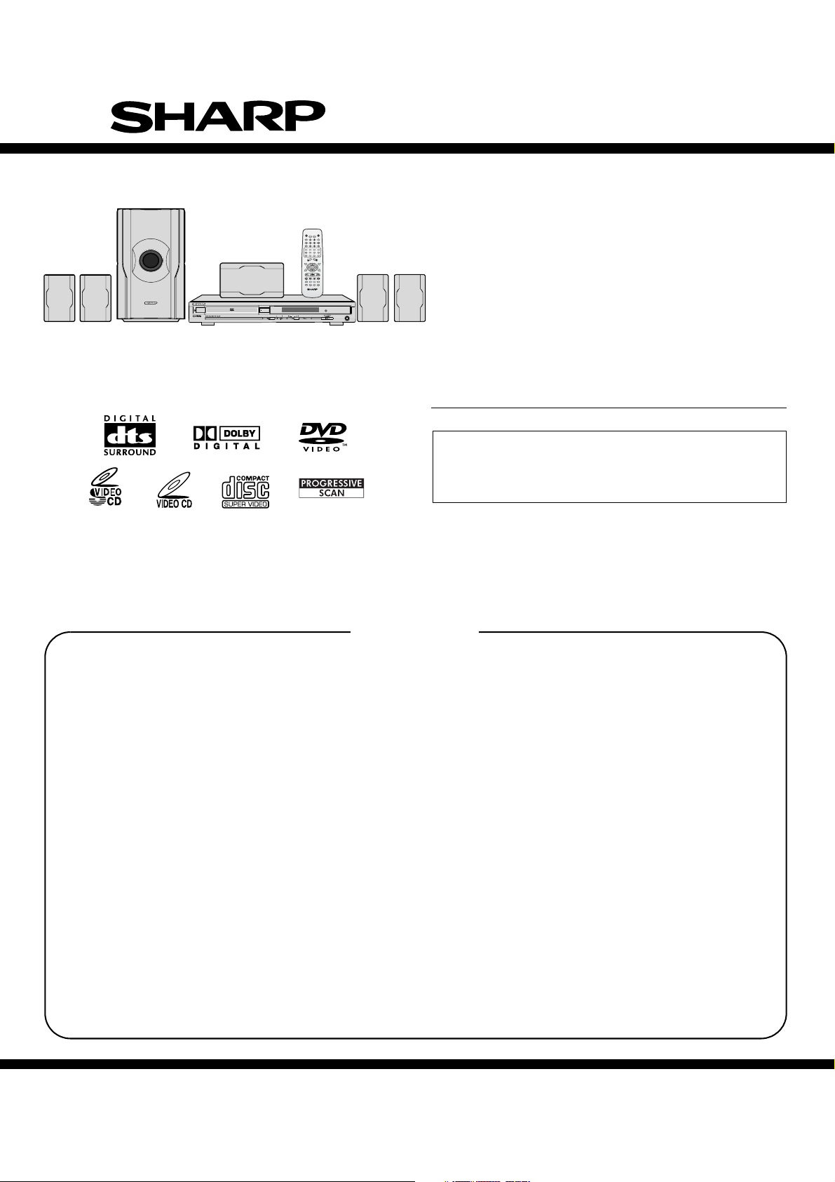
HOME THEATER WITH DVD HT-CN150DVW
MP3
HT-CN150DVW
SERVICE MANUAL
No. S7501HTN150DW
OPEN/CLOSE
ON/STAND BY
FUNCTION
I/P SCAN
MUTE
SLEEP MIC KEY ECHO
DISPLAYDIRECT ZOOM PROG
EQ
LISTENING
REPEAT A-B
ADJ/VOL
MENU/PBCTITLE
ENTER
RETURN
SETUP
SLOW/
PLAY/PAUSE
MEMORY
STOP
V
TUNING
VVPRESET
V
NTSC/PALST/MO MODE
LANGUAGE
STEP ANGLESUBTITLE AUDIO
92LWIR150Z04D7
OPEN /CLOSE
AUDIO/VIDEO
PLAY
MODE
REMOTE
SENSOR
MIC VOLUME
-
SKIP
MIN.
VOLUME
STOPFUNCTION
MAX.
+
MIC
Home Theater with DVD
MODEL
HT-CN150DVW
• In the interests of user-safety (Required by safety regulations in some countries) the set should be restored to its
original condition and only parts identical to those specified
be used.
CONTENTS
Page
SPECIFICATIONS..................................................................................................................................................................2
LASER BEAM SAFETY PRECAUTIONS ..............................................................................................................................4
IMPORTANT SAFEGUARDS AND PRECAUTIONS.............................................................................................................5
STANDARD NOTES FOR SERVICING.................................................................................................................................6
OPERAT ING CONTROLS AND FUNCTIONS......................................................................................................................10
TROUBLESHOOTING..........................................................................................................................................................13
BLOCK DIAGRAMS..............................................................................................................................................................16
SCHEMATIC DIAGRAMS / IC’S PIN VOLTAGE...................................................................................................................18
WAVEFORMS.......................................................................................................................................................................40
WIRING DIAGRAM...............................................................................................................................................................42
SYSTEM CONTROL TIMING CHARTS................................................................................................................................53
IC PIN FUNCTION DESCRIPTIONS....................................................................................................................................54
LEAD IDENTIFICATIONS......................................... ... ........................................................................................................100
FL DISPLAY.........................................................................................................................................................................101
PART GUIDE
SHARP CORPORATION
1
This document has been published to be used for
after sales service only.
The contents are subject to change without notice.
Page 2
HT-CN150DVW
AudioCD-DV999W/CD-DV777WService ManualCD-DV999W/CD-DV777WMarketE
SPECIFICATIONS
As part of our policy of continuous improvement, SHARP reserves the right to make design and specification changes
for product improvement without prior notice. The performance specification figures indicate d are nominal values of production units. There may be some deviations from these values in individual units.
● General
Power source AC 110 - 127 V / 220 - 240 V, 50/60 Hz
Power consumption HT-CN150DVW: Power on: 80 W
Width: 430 mm (17-1/8")
Dimensions
Weight 4.3 kg (9.5 lbs.)
Audio input terminals Analogue input (IN 1): RCA type × 1 pair (L/R)
Audio output terminals Analogue output (OUT): RCA type × 1 pair (L/R)
Video output terminals S-video output: S-terminal × 1 Video output: RCA type × 1
Height: 60 mm (2-3/8")
Depth: 345 mm (13-3/4")
Analogue input (IN 2): RCA type × 1 pair (L/R)
● Amplifier (HT-CN150DVW)
Output power Front speakers: RMS: 60 W (30 W + 30 W) (10 % T.H.D., 1 kHz)
Centre speaker: RMS: 30 W (10 % T.H.D., 1 kHz)
Surround speakers: RMS: 60 W (30 W + 30 W) (10 % T.H.D., 1 kHz)
Subwoofer: RMS: 50 W (10 % T.H.D., 100 Hz)
● DVD player
Signal system PAL/NTSC colour
Supported disc types
Video signal Horizontal resolution: 525 linesS/N ratio: 56 dB
Audio signal Frequency characteristics Linear PCM DVD: 20 Hz to 20 kHz
DVD (with the same region number on the back of the unit or ALL), SVCD, VCD, audio CD,
CD-R, CD-RW, MP3
(sampling rate: 48 kHz)
20 Hz to 20 kHz
(sampling rate: 96 kHz)
CD: 20 Hz to 20 kHz
S/N ratio CD: 65 dB (1 kHz)
Dynamic range Linear PCM DVD: 95 dB CD: 94 dB
Total harmonic distortion ratio 0.2 % maximum
● Tuner
Frequency range FM: 88 - 108 MHz
AM: 531 - 1602 kHz
2
Page 3
● Front speakers
Type Full range speaker system (magnetic shield)
8 cm (3-1/8") speaker
Maximum input power 40 W
Impedance 8 ohms
Dimensions Width: 91.5 mm (3-5/8")
Height: 139.5 mm (5-1/2")
Depth: 100 mm (3-15/16")
Weight 0.7 kg (1.5 lbs.)/each
● Surround speakers
Type Full range speaker system
8 cm (3-1/8") speaker
Maximum input power 40 W
Impedance 8 ohms
Dimensions Width: 91.5 mm (3-5/8")
Height: 139.5 mm (5-1/2")
Depth: 100 mm (3-15/16")
HT-CN150DVW
Weight 0.5 kg (1.1 lbs.)/each
● Center speaker
Type Full range speaker system
8 cm (3-1/8") speaker
Maximum input power 40 W
Impedance 8 ohms
Dimensions Width: 91.5 mm (3-5/8")
Height:169.5 mm (6-11/16")
Depth: 100 mm (3-15/16")
Weight 0.7 kg (1.5 lbs.)
● Subwoofer
Type Subwoofer system
13 cm (5-1/8") Subwoofer
Maximum input power 70 W
Impedance 4 ohms
Dimensions Width:200 mm (7-7/8")
Height: 338 mm (13-9/16")
Depth: 303 mm (12-3/16")
Weight 4.2 kg (9.2 lbs.)
3
Page 4
HT-CN150DVW
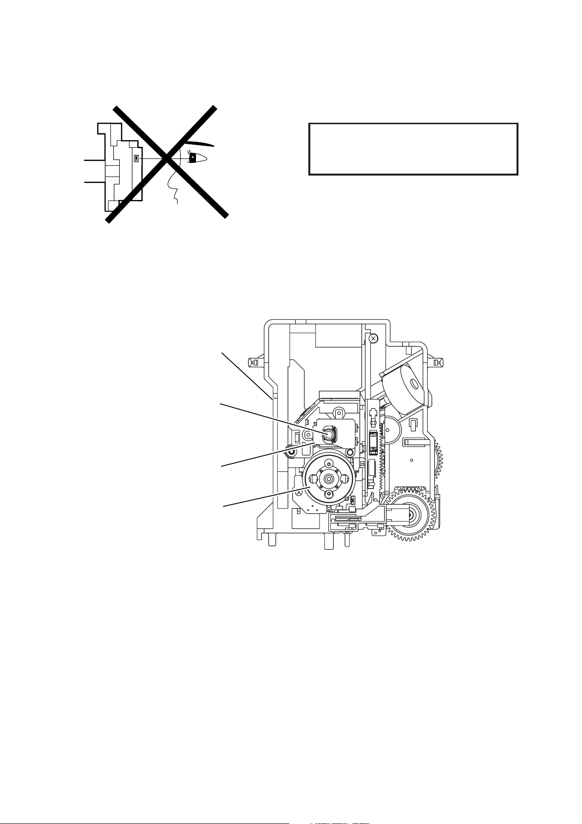
LASER BEAM SAFETY PRECAUTIONS
This DVD player uses a pickup that emits a laser beam.
Do not look directly at the laser beam coming
from the pickup or allow it to strike against
your skin.
The laser beam is emitted from the location shown in the figure. When checking the laser diode, be su re to keep your eyes at least
30cm away from the pickup lens when the diode is turned on. Do not look directly at the laser beam.
Caution: Use of controls and adjustments, or doing procedures other than those specified herein, may result in hazardous radiation
exposure.
Drive Mecha Assembly
Laser Beam Radiation
Laser Pickup
Turntable
4
Page 5
HT-CN150DVW
IMPORTANT SAFEGUARDS AND PRECAUTIONS
1. IMPORTANT SERVICE NOTES
BEFORE RETURNING THE DVD VIDEO PLAYER
Before returning the DVD video player to the user,
perform the following safety checks.
1. Inspect all lead dress to make certain that leads are
not pinched or that hardware is not lodged between
the chassis and other metal parts in the DVD video
player.
2. Inspect all protective devices such as non-metallic
control knobs, insulation materials, cabinet backs,
adjustment and compartment covers or shields,
isola-tion resistor/capacitor networks, mechanical
insula-tors etc.
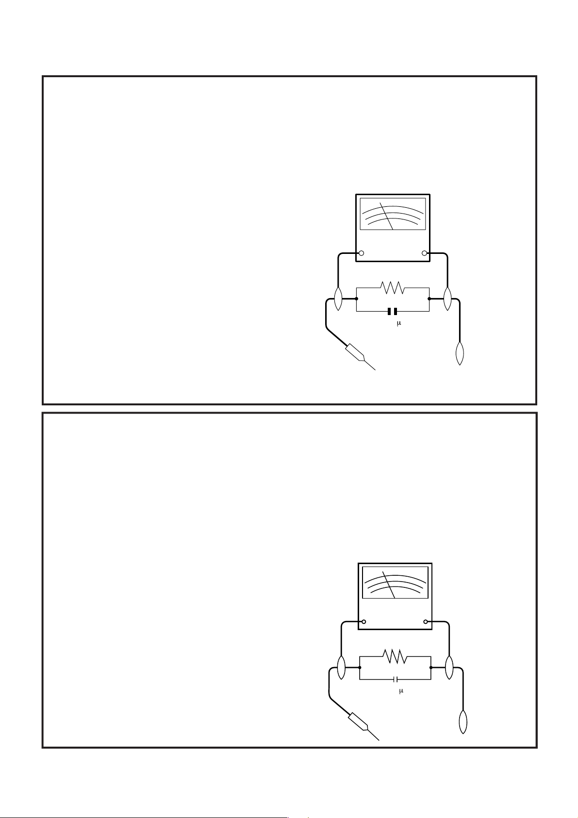
3. To be sure that no shock hazard exists, check for
current in the following manner.
● Plug the AC line cord directly into a 230 volt AC outlet
(Do not use an isolation transformer for this test).
● Using two clip leads, connect a 1.5k ohm, 10 watt
resistor paralleled by a 0.15µF capacitor in series with
all exposed metal cabinet parts and a known earth
ground, such as a water pipe or conduit.
● Use an DVM or VOM with 1000 ohm per volt, or higher,
sensitivity or measure the AC voltage drop across the
resistor (See Diagram).
● Move the resistor connection to earth exposed metal
part having a return path to the chassis (metal cabinet,
screw heads, knobs and control shafts, etc.) and
measure the AC voltage drop across the resistor.
Reverse the AC plug on the set and repeat AC voltage
measurements for each exposed part. Any reading of
1.4V rms (this corresponds to 0.7mA rms AC.) or more
is excessive and indicates a potential shock hazard
which must be corrected before returning the DVD
video player to the owner.
SSVM
AC SCALE
1.5k ohms.
10W
0.15
TEST PROBE
TO EXPOSED
METAL PARTS
F
CONNECT TO
KNOWN EARTH
GROUND
1. NOTES DE SERVICE IMPORTANTES
AVANT DE RENDRE LE REPRODUCTOR DE VÍDEO
DVD
Avant de rendre le reproductor de vídeo DVD à l'utilisateur,
effectuer les vérifications de sécurité suivantes.
1. Vérifier toutes les gaines de fil pour être sûr que les fils
ne sont pas pincés ou que le matériel n'est pas coincé
entre le châssis et les autres pièces métalliques dans le
reproductor de vídeo DVD.
2. Vérifier tous les dispositifs de protection tels que les
boutons de commande non métalliques, les matériaux
d'isolement, le dos du coffret, les couvercles de
compartiment et ajustement ou les boucliers, les
réseaux de résistance / condensateur d'isolement, Ies
isolateurs mécaniques, etc.
3. Pour être sûr qu'il n'y a aucun risque de choc électrique,
vérifier le courant de fuite de la maniére suivante.
● Brancher le cordon d'alimentation secteur directement
dans une prise de courant de 230 volts. (Ne pas utiliser
de transformateur d'isolement pour cet essai).
● Utiliser deux fils à pinces et connecter une résistance de
10 watts 1,5 kohm en parallèle avec un condensateur
de 0,15 F en série avec des pièces du coffret métallique
exposées et une masse de terre connue telle qu'un
tuyau ou un conduit d'eau.
● Utiliser un DVM ou VOM avec une sensibilité de 1000
ohms par volt ou plus ou mesurer la chute de tension
CA entre la résistance (voir diagramme).
● Déposer la connexion de la résistance à toutes les de
pièces métalliques exposées ayant un parcours de
retour au châssis (coffret métallique, tétes de vis,
boutons et arbres de commande, etc.) et mesurer la
chute de tension CA entre la résistance. Inverser la
fiche CA (une fiche intermédiaire non polarisée doit être
utilisée à seule fin de faire ces vérifications.) sur
l’appareil et répéter les mesures de tension CA pour
chaque piéce métallique exposée. Toute lecture de 1,4
V rms (ceci correspond à 0,7 mA rms CA) ou plus est
excessive et signale un danger de choc qui doit être
corrigé avant de rendre le reproductor de vídeo DVD à
son utilisateur.
VTVM
AC SCALE
1.5k ohms
10W
0.15 F
TEST PROBE
TO EXPOSED
METAL PARTS
CONNECT TO
KNOWN EARTH
GROUND
5
Page 6
HT-CN150DVW
STANDARD NOTES FOR SERVICING
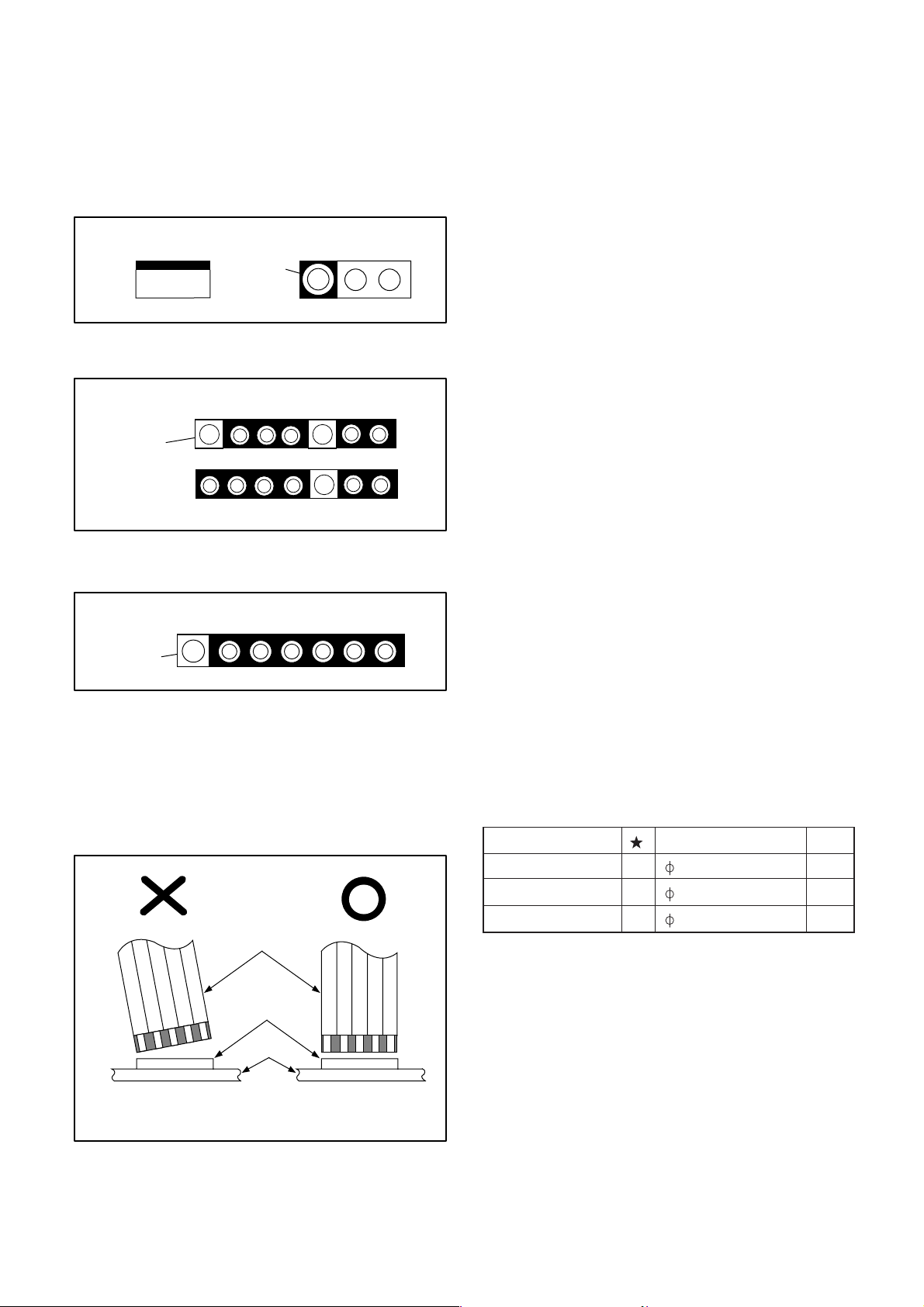
Circuit Board Indications
a. The output pin of the 3 pin Regulator ICs is indicated
as shown.
Top View
Out
b. For other ICs, pin 1 and every fifth pin are indicated
as shown.
< Bottom View >
Input
In
Bottom View
5
Pin 1
10
c. The 1st pin of every male connector is indicated as
shown.
< Bottom View >
Pin 1
Instructions for Connectors
1. When you connect or disconnect the FFC (Flexible
Foil Connector) cable, be sure to first disconnect the
AC cord.
2. FFC (Flexible Foil Connector) cable should be inserted parallel into the connector, not at an angle.
FFC Cable
Using lead-free wire solder
When fixing the PWB soldered with the lead-free solder,
apply lead-free wire solder. Repairing with conventional
lead wire solder may cause damage or accident due to
cracks.
As the melting point of lead-free solder (Sn-Ag-Cu) is
higher than the lead wire solder by 40°C, we recommend
you to use a dedicated soldering bit, if you are not
familiar with how to obtain lead-free wire solder or
soldening bit, contact our service station or service
ranch in your area.
Soldering
As the melting point of lead-free solder (Sn-Ag-Cu) is
about 220°C which is higher than the conventional lead
solder by 40°C, and as it has poor solder wettabillty, you
may be apt to keep the soldering bit in contact with the
PWB for extended period of time. However, Since the
land may be peeled off or the maximum heat-resistance
temperature of parts may be excoeded, remove the bit
from the PWB as soon as you conurm the steady
soldering condition.
Lead-free solder contains more tin, and the end of the
soldering bit may be easily corroded. Make sure to tum
on and off the power of the bit as required. if a different
type of solder stays on the tip of the soldering bit, it is
alloyed with lead-free solder. Clean the bit after every
use of it.
When the tip of the soldering bit is blackened during
use, file it with steel wool or fine sandpaper.
Becareful when replacing parts with polarity indication
on the PWB silk.
Lead-free wire solder for servicing
Part No.
ZHNDAi123250E J
ZHNDAi126500E J
ZHNDAi12801KE J
Description Code
0.3mm 250g(1roll) BL
0.6mm 500g(1roll) BK
1.0mm 1kg(1roll) BM
Connector
CBA
* Be careful to avoid a short circuit.
6
Page 7
HT-CN150DVW
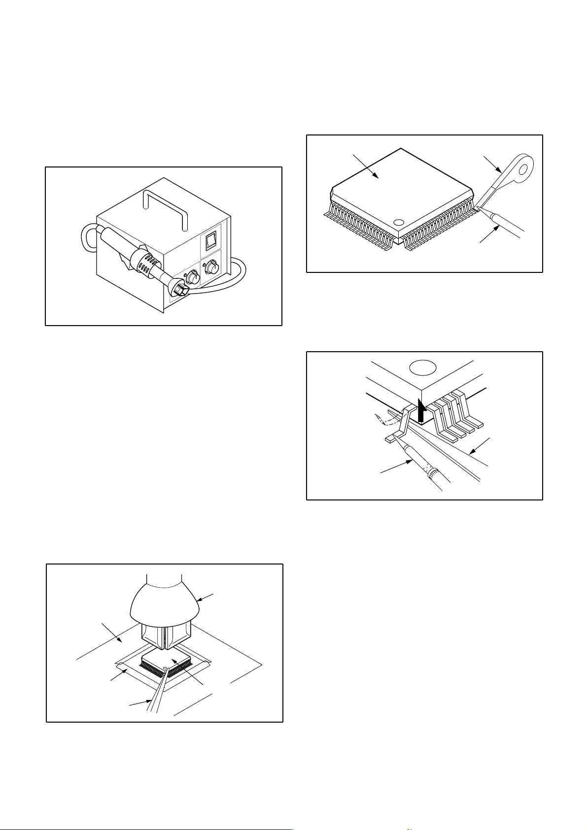
How to Remove / Install Flat Pack-IC
1. Removal
With Hot-Air Flat Pack-IC Desoldering Machine:
(1) Prepare the hot-air flat pack-IC desoldering ma-
chine, then apply hot air to the Flat Pack-IC (about 5
to 6 seconds). (Fig. S-1-1)
Fig. S-1-1
(2) Remove the flat pack-IC with tweezers while apply-
ing the hot air.
(3) Bottom of the flat pack-IC is fixed with glue to the
CBA; when removing entire flat pack-IC, first apply
soldering iron to center of the flat pack-IC and heat
up. Then remove (glue will be melted). (Fig. S-1-6)
(4) Release the flat pack-IC from the CBA using twee-
zers. (Fig. S-1-6)
Caution:
1. Do not supply hot air to the chip parts around the flat
pack-IC for over 6 seconds because damage to the
chip parts may occur. Put masking tape around the
flat pack-IC to protect other parts from damage.
(Fig. S-1-2)
2. The flat pack-IC on the CBA is affixed with glue, so
be careful not to break or damage the foil of each pin
or the solder lands under the IC when removing it.
Hot-air
Flat Pack-IC
Desoldering
CBA
Masking
Tape
Tweezers
Machine
Flat Pack-IC
Fig. S-1-2
With Soldering Iron:
(1) Using desoldering braid, remove the solder from all
pins of the flat pack-IC. When you use solder flux
which is applied to all pins of the flat pack-IC, you can
remove it easily. (Fig. S-1-3)
Flat Pack-IC
Desoldering Braid
Soldering Iron
Fig. S-1-3
(2) Lift each lead of the flat pack-IC upward one by one,
using a sharp pin or wire to which solder will not
adhere (iron wire). When heating the pins, use a fine
tip soldering iron or a hot air desoldering machine.
(Fig. S-1-4)
Sharp
Pin
Fine Tip
Soldering Iron
Fig. S-1-4
(3) Bottom of the flat pack-IC is fixed with glue to the
CBA; when removing entire flat pack-IC, first apply
soldering iron to center of the flat pack-IC and heat
up. Then remove (glue will be melted). (Fig. S-1-6)
(4) Release the flat pack-IC from the CBA using twee-
zers. (Fig. S-1-6)
With Iron Wire:
(1) Using desoldering braid, remove the solder from all
pins of the flat pack-IC. When you use solder flux
which is applied to all pins of the flat pack-IC, you can
remove it easily. (Fig. S-1-3)
(2) Affix the wire to a workbench or solid mounting point,
as shown in Fig. S-1-5.
(3) While heating the pins using a fine tip soldering iron
or hot air blower, pull up the wire as the solder melts
so as to lift the IC leads from the CBA contact pads
as shown in Fig. S-1-5.
7
Page 8
HT-CN150DVW
(4) Bottom of the flat pack-IC is fixed with glue to the
CBA; when removing entire flat pack-IC, first apply
soldering iron to center of the flat pack-IC and heat
up. Then remove (glue will be melted). (Fig. S-1-6)
(5) Release the flat pack-IC from the CBA using twee-
zers. (Fig. S-1-6)
Note:
When using a soldering iron, care must be taken to
ensure that the flat pack-IC is not being held by glue.
When the flat pack-IC is removed from the CBA,
handle it gently because it may be damaged if force
is applied.
Hot Air Blower
or
Iron Wire
Soldering Iron
2. Installation
(1) Using desoldering braid, remove the solder from the
foil of each pin of the flat pack-IC on the CBA so you
can install a replacement flat pack-IC more easily.
(2) The "●" mark on the flat pack-IC indicates pin 1. (See
Fig. S-1-7.) Be sure this mark matches the 1 on the
PCB when positioning for installation. Then presolder the four corners of the flat pack-IC. (See Fig. S1-8.)
(3) Solder all pins of the flat pack-IC. Be sure that none
of the pins have solder bridges.
Example :
Pin 1 of the Flat Pack-IC
is indicated by a " " mark.
Fig. S-1-7
To Solid
Mounting Point
CBA
Tweezers
Fig. S-1-5
Fine Tip
Soldeing Iron
Flat Pack-IC
Fig. S-1-6
Presolder
Flat Pack-IC
CBA
Fig. S-1-8
8
Page 9
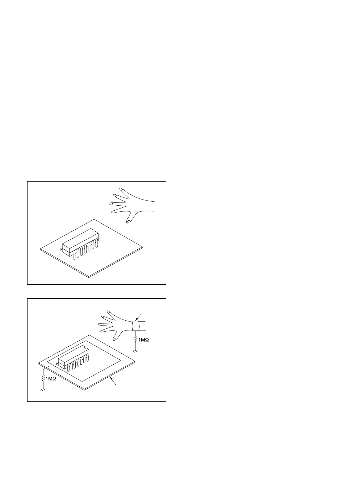
Instructions for Handling
Semi-conductors
Electrostatic breakdown of the semi-conductors may
occur due to a potentialdifference caused by electrostatic
charge during unpacking or repair work.
1. Ground for Human Body
Be sure to wear a grounding band (1MΩ) that is properly
grounded to remove any static electricity that may be
charged on the body.
2. Ground for Workbench
Be sure to place a conductive sheet or copper plate with
proper grounding (1MΩ) on the workbench or other
surface, where the semi-conductors are to be placed.
Because the static electricity charge on clothing will not
escape through the body grounding band, be careful to
avoid contacting semi-conductors with your clothing.
< Incorrect >
HT-CN150DVW
< Correct >
CBA
Grounding Band
CBA
Conductive Sheet or
Copper Plate
9
Page 10
HT-CN150DVW
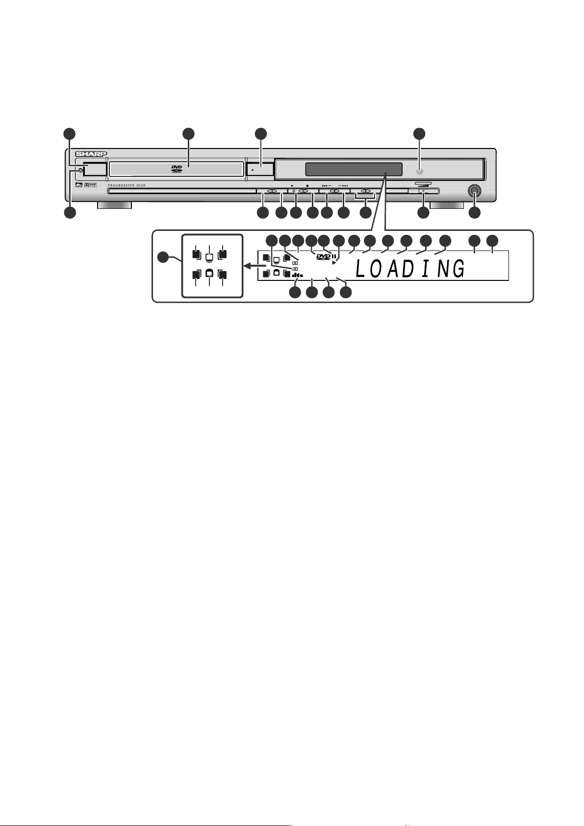
OPERATING CONTROLS AND FUNCTIONS
■ Main unit (front panel)
1
HOME THEATERWITH DVD HT-CN150DVW
ON/ STAND-BY
MP3
2 3 4
OPEN/CLOSE
5 6 8 9
(1)
(3)(2)
RL
(4) (6)(5)
C
S
RSLS
15
1. On/Stand-by Button
2. Disc Tray
3. Disc Tray Open/Close Button
4. Remote Sensor
5. Power Stand-by Indicator
6. Function Button
7. Speaker Level Mode Button
8. Play or Pause Button
9. Stop Button
10. Chapter (track) Skip Down or Preset/Tuning Down Button
11. Chapter (track) Skip Up or Preset/Tuning Up Button
12. Volume Up and Down or Speaker Level Adjust Buttons
13. Microphone Volume Control
14. Microphone Socket
15. Speaker Indicators
(1) Left Front Speaker Indicator
(2) Centre Speaker Indicator
(3) Right Front Speaker Indicator
(4) Left Surround Speaker Indicator
(5) Subwoofer Indicator
(6) Right Surround Speaker Indicator
PLAY STOPFUNCTION
16 17 18
RL
C
S
RSLS
30 31 32 33
REMOTE
SENSOR
-
VOLUMESKIPMODE
+
12
MICVOLUME
MIN.
MAX.
137 10 1411
242319 20 21 22
DIGITAL
Pro Logic
CD MP3STEREO V
16. Dolby Pro Logic Indicator
17. Dolby Digital Signal Indicator
18. P - SCAN mode
19. DVD Indicator
20. Pause Indicator
21. Play Indicator
22. Title Indicator
23. Track Indicator
24. Tuner Preset Indicator
25. Chapter Indicator
26. Programme Indicator
27. Sleep Indicator
28. Repeat Indicator
29. A - B Repeat Indicator
30. DTS Signal Indicator
31. Stereo (2-ch) or FM Stereo Receiving Indicator
32. SVCD/VCD/CD Indicator
33. MP3 or JPEG Indicator
REPEAT 1SLEEPPROGCHPPRESETTRKTITLEP-SCAN
MIC
2928272625
A-B
KHz
MHz
10
Page 11
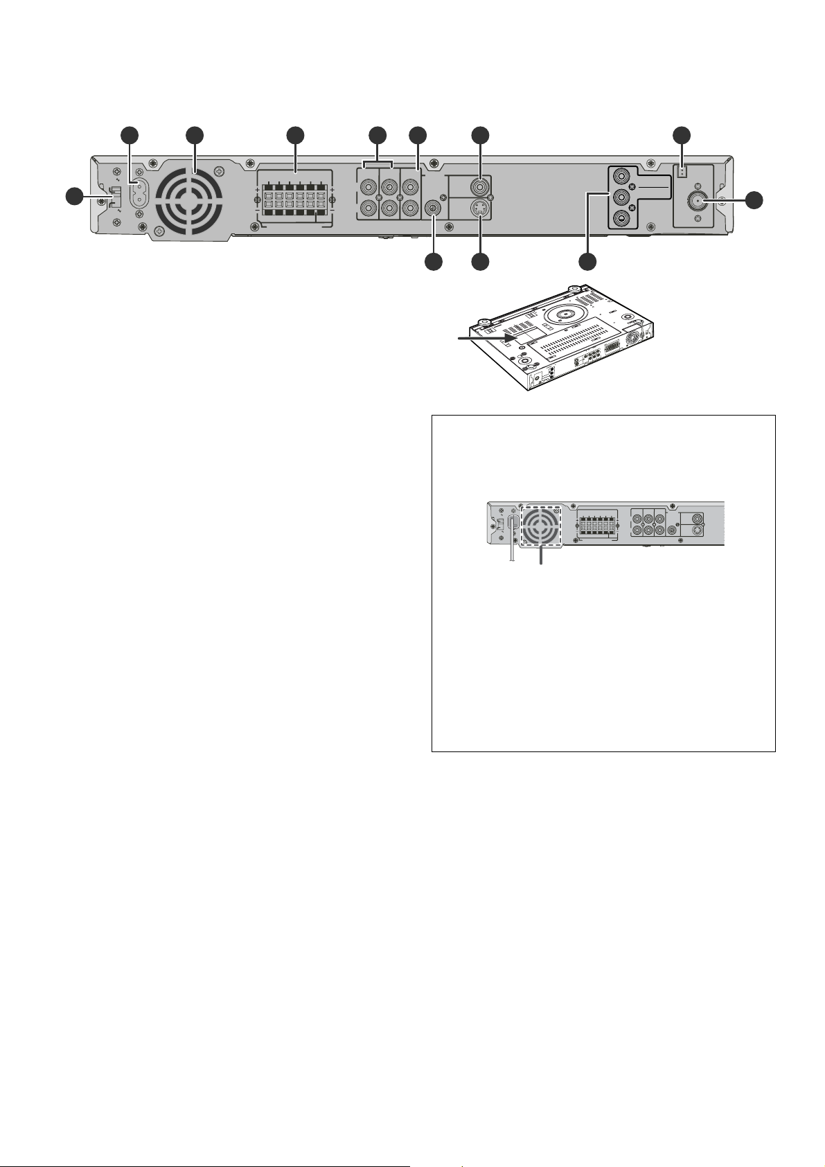
■ Main unit (rear panel)
n
h
S
r
o
D
HT-CN150DVW
AC
INPUT
110
127V
8
220
240V
The rating label is located on the bottom of the unit.
1. AC Power Input Socket
2. Cooling Fan
3. Speaker Terminals
4. Audio Input Sockets (TV/AUX)
5. Audio Output Sockets
6. Video Output Socket
7. AM Loop Aerial Socket
8. AC Voltage Selector
9. Digital Output Socket (Coaxial)
10. S-video Output Socket
11. Component Video output Sockets
12. FM 75 Ohms Aerial Socket
3 5 6 721
SURROUND
FRONT
MINIMUM RATED SPEAKERIMPEDANCE
WOOFER
CENTER
RR
LL
8OHMS 4OHMS
4
AUDIO
SUB
AUX
L
R
DIGITAL
OUT
INTVIN
AUDIO OUT
VIDEO
OUT
COAXIAL
S-VIDEO
OUT
9
Manufactured under license from Dolby Laboratories.
"Dolby", "Pro Logic" and the double-D symbol are
trademarks of Dolby Laoratories.
Manufactured under license from Digital Theater Systems,
lnc. US Pat. No . 5,451,942, 5,956,674, 5,974,380,
5,978,762 and other world-wide patents issued and pending
."DTS" and "DTS Digital Surround" are registered trademarks
of Digital Theater Systems, Inc. Copyright 1996,2000
Digital Theater Systems, Inc. All rights reserved.
10
11
P
R
COMPONENT
P
b
Y
VIDEO OUT
AM
75 OHMS
FM
ANTENNA
12
Cooling fan
This unit is fitted with a cooling fan at the rear for improved
cooling. Do not cover the opening in this section with any
obstacles.
AUDIO
AC
INPUT
110
127V
220
240V
SURROUND
FRONT
CENTER
RR
8 OHMS 4 OHMS
MINIMUM RATED SPEAKER IMPEDANCE
AUXINTV
SUB
WOOFER
LL
DIGITAL
OUT
IN
AUDIO OUT
L
COAXIAL
R
Manufactured u
"Dolby", "Pro L
VIDEO
trademarks of
OUT
Manufactured u
lnc. US Pat. No .
S-VIDEO
5,978,762 and ot
OUT
."DTS" and "DT
of Digital Theate
Digital Theater S
cooling fan
Caution:
● The unit will get warm whilst being used. Do not touch
the warm areas of the unit for prolonged periods to avoid
damage to you.
● This unit is equipped with a special function which protects the amplifier circuit from damages. When it is activated, the sound switch is turned off. In this case,
unplug the unit and, after 15 minutes or more, plug it in
again.
11
Page 12
HT-CN150DVW
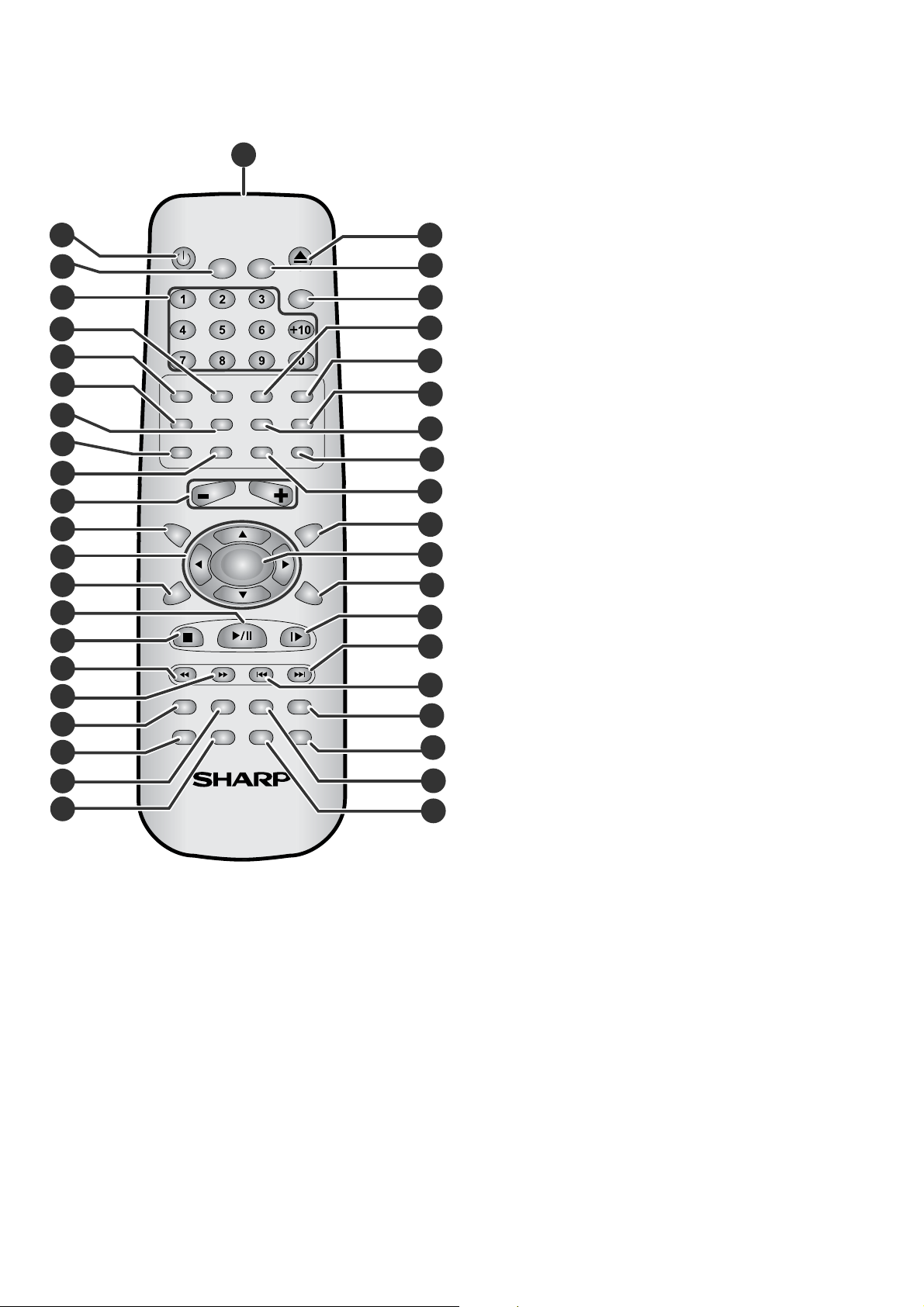
■ Remote Control
2
ON/STAND BY
FUNCTION
3
4
5
6
7
8
9
SLEEP MIC KEY ECHO
DISPLAY DIRECT ZOOM PROG
EQ
LISTENING
10
11
12
13
14
SETUP
15
STOP
16
V
TUNING
17
18
19
NTSC/PAL ST/MO MODE
STEP ANGLE SUBTITLE AUDIO
20
21
92LWIR150Z04D7
22
1
I/P SCAN
REPEAT A-B
ADJ/VOL
ENTER
PLAY/PAUSE
V
LANGUAGE
OPEN/CLOSE
MEMORY
PRESET
V
MUTE
MENU/PBCTITLE
SLOW/
RETURN
V
23
24
25
26
27
28
29
30
31
32
33
34
35
36
37
38
39
40
41
1. Remote Control Transmitter
2. On/Stand-by Button
3. Function Button
4. Direct Number Buttons
5. Mic Button
6. Sleep Button
7. Display Button
8. Direct Button
9. EQ (equalizer) Button
10. Surround/Stereo (2-ch) Listening Mode Button
11. Volume Up and Down or Speaker Level Adjust Buttons
12. Title Select Button
13. Cursor Buttons
14. Set Up Menu Button
15. Play or Pause Button
16. Stop Button
17. Fast Reverse or Tuning Down Button
18. Fast Forward or Tuning Up Button
19. NTSC/PAL Select Button
20. Frame Advance Button
21. FM Stereo/Mono Select Button
22. Angle Select Button
23. Disc Tray Open/Close Button
24. Interlace and Progressive Scan Button
25. Mute Button
26. Key Button
27. Echo Button
28. Programme Button
29. Zoom Button
30. A - B Repeat Button
31. Repeat Play Button
32. Menu/Playback /Control On/Off Button
33. Enter Button
34. Return Button
35. Slow Motion/Memory Button
36. Chapter (track) Skip Up or Preset Up Button
37. Chapter (track) Skip Down or Preset Down Button
38. Speaker Level Mode Button
39. Audio Select Button
40. Language Select Button
41. Subtitle Select Button
12
Page 13
TROUBLESHOOTING
HT-CN150DVW
AM FM
KL
Cannot Read The
Ear Head Phone
SCART SUB OUT
AV CONNECTOR
G
S-Video
MAIN UNIT REPAIR CHART
Video
OPTICAL
DF
AUDIO L/R
B
No Output
Disc Or Intermittent
No Sound
No Output
No Output
No Output
No Output
No Output
No Output
No Show
VFD Display
And Key Function
the cable
RE-Insert and fix
No
Yes
Check Control Board
CN201 CN202
Cable loose or bad INT
Check Main Board
IC953 or IC953 periphery
IC208 or IC208 periphery
NO
Check Main Board
YES
NO
PIN5 -24 V
Check CN902 voltage
PIN1 6.8VPIN7 8 AC
PIN3 12VPIN2 4 6 GND
YES
Repair power
Supply circuit
No
PIN12 5V
Pin13 12V-16V
Check RB201
Pin7 8 : AC Pin 6: -24V Pin5 5V
YES
IC201 or IC201 periphery
IC801 or IC801 periphery
YES
IC953 PIN3 5 V
YES
Board
Check Power
Check Main Board
IC954 or IC954 periphery
NO
Repair between the
Yes
Check Control
Repair
IC208 circuit
IC209 circuit short
IC201 pin short 1 10 19
35 44 53 62 96 104 185
IC202 pin short 13 14 27
IC201 pin short1 3 9 14 27 43 49
NO
IC208PIN3 3.3V
Check Main Board
Repair
170 ircuit short
IC210 circuit
IC201 pin 147 152
IC351 pin 5 ircuit short
IC801 pin 35 47 ircuit short
NO
IC210 PIN3 3.3V
Check Main Board
to IC953 PIN3 return
Check C285 anode
NO
C285 Anode 5V
Check Main Board
Repair
IC505 peri phery
IC405 PIN 42 circui t short
CN201 PIN 5 circui t short
IC205 or I C205 periphery
NO
IC202A Circuit
to VFD Display
Main board IC201
No
Yes
Pin9:STB
Pin8:CLKPin5 6: Data
IC202A ( Data,CLK,STB )
Repair
RA201 IC204 circuit short
IC201 circuit
XL201 circuit
IC201 pin short1 3 9 14 27 43 49
NO
t
YES
YES
YES
YES
Check Main Board
frequency 27MHZ)
IC 201 PIN20(OSC
IC201 PIN207=Rese
Renewal bastard
NO
Check
Confirm IC801
IC201 IC351 OK
IC801 IC201 IC351
IC801
Check
PIN 19 58 circuit open
IC201A
to RB201 Return
Repair between the
No
Yes
Check Control
IC201A ( PIN 12 Voltage)
Repair
IC105Circuit
NO
IC204 PIN3 =3.3V
Check Main Board
YES YES
Renewal IC201A
Repair XL301 Circuit
No
Yes
XL301 Check
Check IC201A Fettle
(OSC frequency 455KHZ)
Circuit IC201 t o IC202
NO
YES
IC20 2 F ix softw re
YES
Check Main Board
8
Check
IC301 Circuit
Circuit IC201 t o IC203
Renewal bastard
NO
YES
Check
Check IC110
IC201 IC202
Check IC110 PIN51 DSCK signal
7
IC203 circuit
CE
No Output
5.1-CH.STEREO
BHA IJ
No Show
VFD Display
A
And Key Function
All Function
No Working
Repair F1
A
All function
No Working
B
TROUBLESHOOTING CHART (1/3)
Check Main Board
Repair
Yes
Power T901
or bad INT
All cable is loose
Check All System
Yes
the cable
RE-Insert and fix
YES
IC954 PIN3 5 V
Circuit
No
Test CN903 PIN2
No
No
Panel stanby LED
13
IC205 PIN8 5V
Check Main Board
20>STB>12V
Yes
Check Main Board
show Working or Not
No
Repair
Control Board
IC 201A circuit
C
Yes
12V<PIN4<16V
CN202PIN4:
(HT48R05A)
Supply circuit
Repair power
Yes
5V
CN202PIN3:
Check Main Board
No
D
Yes
CN903PIN1
3.5V
Check Main Board
No
Boaed
Check Power
23456
1
E
Page 14
HT-CN150DVW
K
AM FM
No Output
JH
Cannot Read The
Disc Or Intermittent
I
MIC IN
No Sound
G
AUDIO OUT COAXIAL
No Output
the cable
RE-Insert and fix
NO
or bad INT
Check Main Board
JK804 cable is loose
Yes
Check Main Board
NO
C257 signal output
H
Filter Circuit
IC201 Pin114 to C257
Check Main Board Between
NO
No Output
COMPONET VIDEO
Check Main Board
the cable
RE-Insert and fix
Yes
or bad INT
JK806 cable is loose
CN804 signal output
Check Main Board
NO
Filter Circuit
Check Main Board Between
IC201 Pin113 114 1125 to CN804
8
7
No Sound
COMPONET VIDEO
G
No Output
AUDIO OUT COAXIAL
FB
S-Video
No Output
MAIN UNIT REPAIR CHART
E
Video
No Output
D
No Output
AUDIO L/R
C
No Output
5.1-CH.STEREO
RE-Insert and fix
NO
Check Main Board
JK801 cable is loose
IC401 to IC404
Check Between
YES
No
signal output
IC401 Pin1 7
the cable
Yes
or bad INT
Check
Check IC401
IC401 voltage Circuit
YES
No
signal IN
IC401 Pin2 6
Check Main Board
Check Main Board
L812 L813 signal output
Check
Check IC351
CheckI351 to IC401
IC351 voltage Circuit
YES
IC351
signal IN
Check Main Board
NO
Filter Circuit
Check Main Board Between
IC201 Pin112 113 to L812 L813
Yes
Check
L809 to JK101
Between Main Board
Yes
NO
L809 signal output
Check Main Board
D
No Output
AUDIO L/R
F
Check Main Board Between
IC201 Pin110 to L809 CIRCUIT
Check
Check Between
IC406 TO JK401
YES
signal output
IC406 Pin1 7
Check Main Board
Check IC406
IC406 voltage Circuit
YES
No
signal IN
IC406 Pin2 6
Check Main Board
S-Video
No Output
No
Check Main Board
the cable
RE-Insert and fix
NO
E
Video
No Output
or bad INT
Check Main Board
JK802 cable is loose
VFD Display
A
All Function
A
No Show
And Key Function
No Working
C
No Output
5.1 - CH.STEREO
B
JK501 Circuit
IC501-IC503 to
Repair
Power Supply
No
Check CN901
Check Main Board
Check Between
Yes
Yes
Pin16 SL OUT
Pin16 L OUT
Pin21 SR OUT
Check Main Board
PIN1=+28VPIN3=GND
OP IC Audio signal output
IC 501
Pin21 R OUT
Pin16 C OUT
Pin21 SW OUT
IC502
IC503
Confirm mainframe mute off
Check Main Board mute circuit
Low
No
IC501-503
Mute Return circuit
Check Main Board
High
C
TROUBLESHOOTING CHART (2/3)
14
Renewal bastard
No
Yes
Confirm Speake
Confirm IC501-503 fettle
Gradually disturb each import
Confirm every IC supply power
Check Main Board
UP to C315-350 anode
IC351 supply power Check Between
D
Confirm IC201 fettle
IC201 to IC351 Circuit
No
Yes
Check IC351 PIN3 BCLK
Check IC351 PIN4 LRCK
Check IC351 PIN7 DIN1
Check IC351 PIN8 DIN2
Check IC351 PIN3 DIN3
Check IC351 PIN2 MCLK
Confirm IC351 fettle
Check Main Board
E
23456
1
Page 15
HT-CN150DVW
L
AM FM
No Output
K
Cannot Read The
J
EarHead Phone
I
No Output
SCART SUB OUT
H
No Output
AV CONNECTOR
G
S-Video
No Output
MAIN UNIT REPAIR CHART
F
Video
No Output
E
OPTICAL
No Output
D
No Output
AUDIOL/R
C
No Output
5.1-CH.STEREO
B
No Show
VFD Display
A
AllFunction
No Working
Disc Or Intermittent
No Sound
K
AndKey Function
Cannot Read The
Disc Or Intermittent
NO DISC STATUS
RE-Insert and fix
NO
Check Main Board
CN801 CN803 CN812 CN813
CN 812 PIN1 = PIN2
CN 813 PIN1234=0V
CN 803 PIN1 3V
CN 803 PIN2 0V
the cable
cable is loose or bad INT
the cable
RE-Insert and fix
NO
L
AM FM
No Output
CN 812 PIN1 = PIN2
PLAY STATUS
CN 803 PIN1 4V
CN 803 PIN2 6.5V
CN 803 PIN4 = CN803 PIN5
CN 803 PIN3 0V
CN 803 PIN1 3V
CN 803 PIN2 0V
ANT001 CN002
Check Main Board
cable is loose or bad INT
Repair IC804801 circuit
NO
CN801 NO
CN 803 PIN4 2.3V
CN 803 PIN3 0V
CN 803 PIN3 0V
CN 803 PIN4 = CN803 PIN5
Change IC 804 ci ruit
Change IC801 ciruit
Repair IC802
Repair IC802 circuit
Check Main Board
NO
Yes
CN 151
Check Main Board
Q813 around circuit
Repair Q800-803811
YES
Change 0805 0806 ciruit
around circuit
IC201 Signal
Supply Power
Voltage Circuit signal IN
PIN4 12V PIN5 6 7 8 signal
8
7
NO
the cable
RE-Insert and fix
NO
Change IC802
YES
Yes
Check Main Board
CN801 signal IN
C813 CN803CN812 voltage
Loader is OK?
NO
Change Loader
CN813 NO CN812 NO
CN803 NO
Repair IC201
around circuit
Repair IC201circuit
NO
118 Signal
Change IC802
Chan g e IC2 0 1Pin 117
Repair IC802
around circuit
Repair IC802 circuit
NO
Change IC802
YES
YES
Check Main Board
IC801 and IC201 connect
NO DISC STATUS CD PLAY STATUS
Pin14
Pin13
Pin12
Pin11
Pin9 Pin10
Pin8
Pin7
Pin6
Pin5
Pin4
Pin3
Pin2
Pin1
0V
2.5V
Pin14
Pin13
Pin12
Pin11
Pin10
Pin8
Pin7 Pin9
Pin6
Pin5
Pin4
Pin3
Pin2
Pin1
2.3V
2.5V
1.5V
Pin27 Pin28
5.6V
1.5V
Pin26
2.5V
Pin25
2.5V
5.2V11V 5.5V
Pin24
5.2V
1.3V
0
Pin22
0V
11V
Pin21 Pin23
0V
2.5V
Pin20
5V
2.5V
Pin19
6.4V
1.5V
Pin18
2.5V
2.5V 4.7V
2.5V
Pin16 Pin17
2.5V
1.5V
Pin15
2.5V
Pin28
2.5V
1.5V
Pin27
1.5V
6.1V
Pin26
2.5V
Pin25
Pin24
1.5V 2.5V0V
Pin23
Pin22
0V 1.2V 1.5V12V 6.1
12V
Pin21
0V
2.5V
Pin20
5V
2.5V
Pin19
3.6V
1.5V
Pin18
2.5V
Pin17
2.5V
2.5V 3.6V
Pin16
2.5V
1.5V
Pin15
23456
IC803A PIN3 return
ControlJK301 IC803A
1
Confirm Speaker
the cable
the cable
RE-Insert and fix
NO
H
MIC IN
No Output
Check Main Board
or bad INT
JK 301 cable is loose
A
RE-Insert and fix
NO
Yes
or bad INT
Check Main Board
CN 801B cable is loose
B
5.1 - CH.STEREO
Check Main Board
No Output procedure
NO
Yes
DisturbCN801B PIN12
ConfirmSpeaker
Yes
CN801A TO CN801B
Check Main Board Between
C
Renewalbastarf
ConfirmIC802A Periphery
No
Yes
Yes
Check MIC Board
Disturb IC802APIN35 Confirm Speaker
Confirm IC801A802A803A Supply power
Check Between
IC 802A PIN35 to
IC 803APIN7return
No
ConfirmSpeaker
Check MICBoard
DisturbIC803A PIN7
D
Check Between
Yes
IC801A PIN15 to
No
Check MICBoard
ControlIC802A
IC803APIN5 return
Confirm Speaker
Disturb IC801A PIN 15
Check Between
Yes
Check MICBoard
E
RB 855B to
No
DisturbRB855B
TROUBLESHOOTING CHART (3/3)
15
Page 16
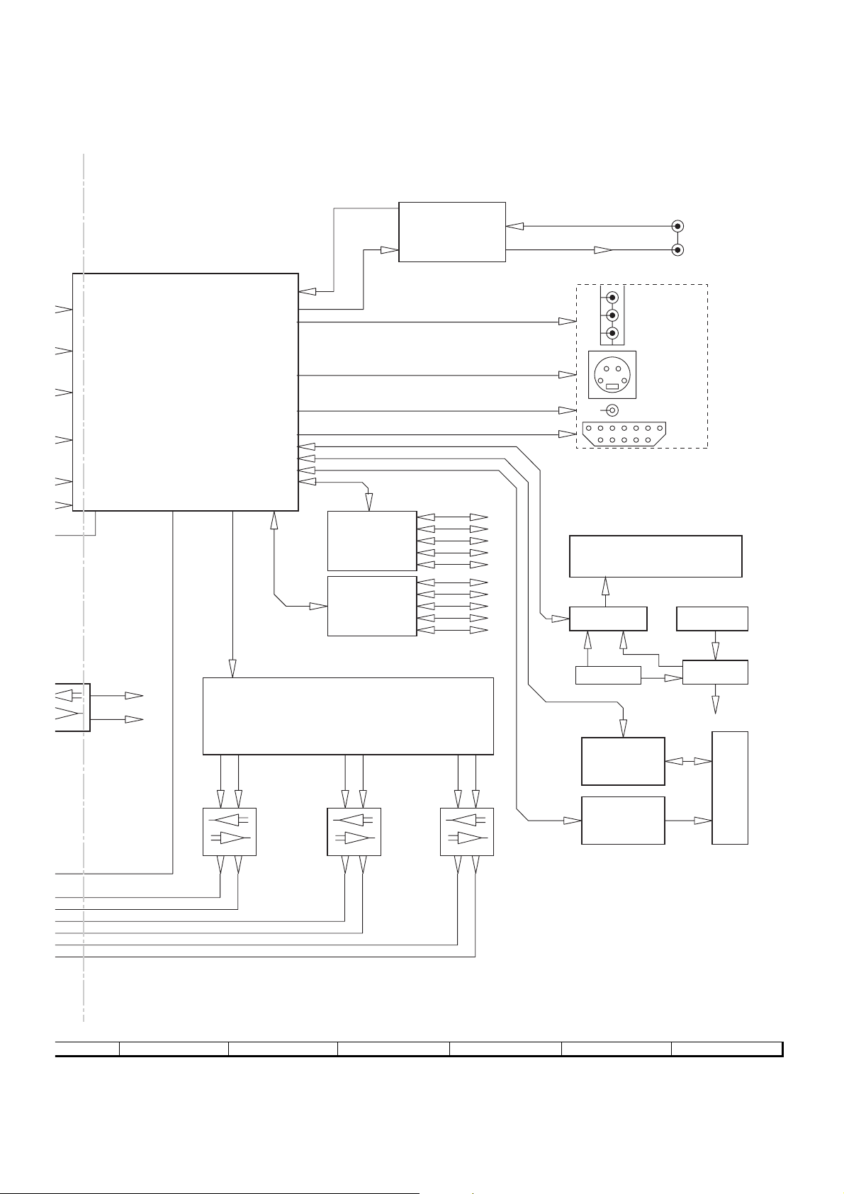
HT-CN150DVW
A
B
AC input 120V/230V
POWER
SUPPLY
BLOCK DIAGRAM
+12V
-12V
+5V
+6.8V
PCON
-24V
3.6V AC
GND
+5V_STB
TEA5762H+SAA6588T
RADIO PACK
FM IN
AM IN
RESET
FLASH
SST39VF080
L
C
R
TV-INTV-IN
SDRAM
4MX16
IC TC4052B
L
R
D
L
R
AUX-IN
L CH
R CH
IC RC4558D
2*14W OUT
IC TDA7269
IC AT24C02
SERIAL EEPROM
27MHZ
E
L
LINE OUT
SUB
C
F
2*25W OUT
IC TDA7265
IC RC4558D
IC RC4558D IC RC4558D IC RC4558D
R
SL
2*14W OUT
SR
IC TDA7269
L
IC M6244FP
R
G
MIC IN
IC PT2399 VR
IC RC4558D
IC RC4558D
H
1
23456
BLOCK DIAGRA3M (1/2)
16
Page 17
HT-CN150DVW
ES6629FD
IC 74HC374
IC 74HC374
IC 74HC04
IO-PUT
IO-PUT
VFD(DR1060)
IC HT16511
SPDIF-IN
SPDIF-OUT
Y.V.U OUT
S-VIDEO
C-VIDEO
SCART
KEY
C4558D
6
L
LINE OUT
R
IC WM8772
D/A EXCHANGE
L CH
R CH
IC RC4558D IC RC4558D IC RC4558D
7
8 9 10 11 12
C CH
SUB CH
BLOCK DIAGRAM (2/2)
SL CH
SR CH
IR
IC EC6603
(RF)
AT5660
(DRIVER)
HT48R05
PCON
RA0
M02
DVD LOADER
17
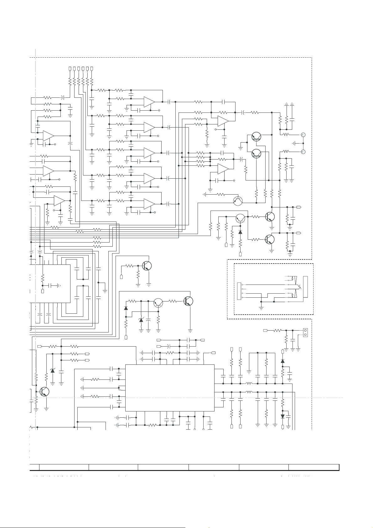
Page 18
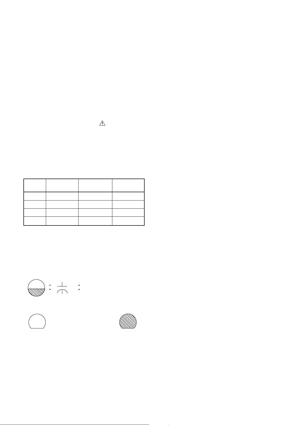
HT-CN150DVW
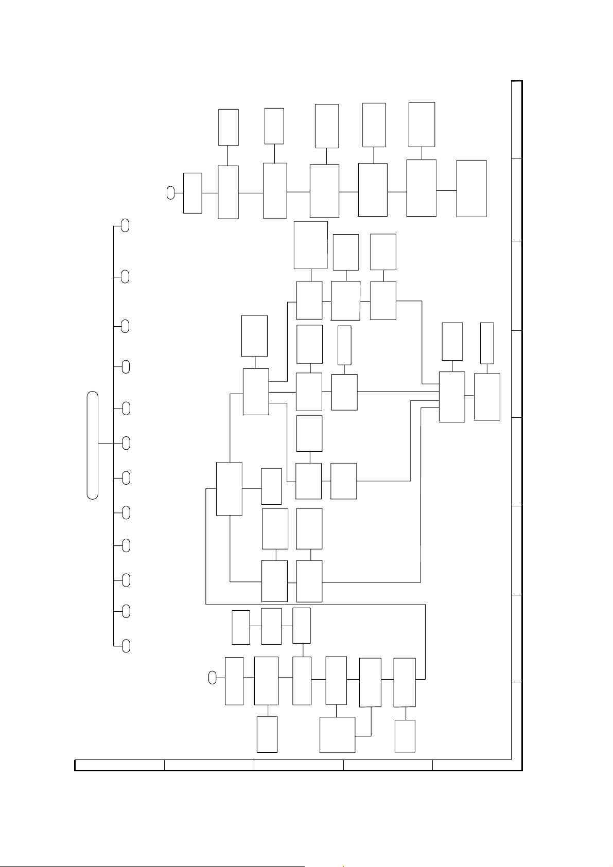
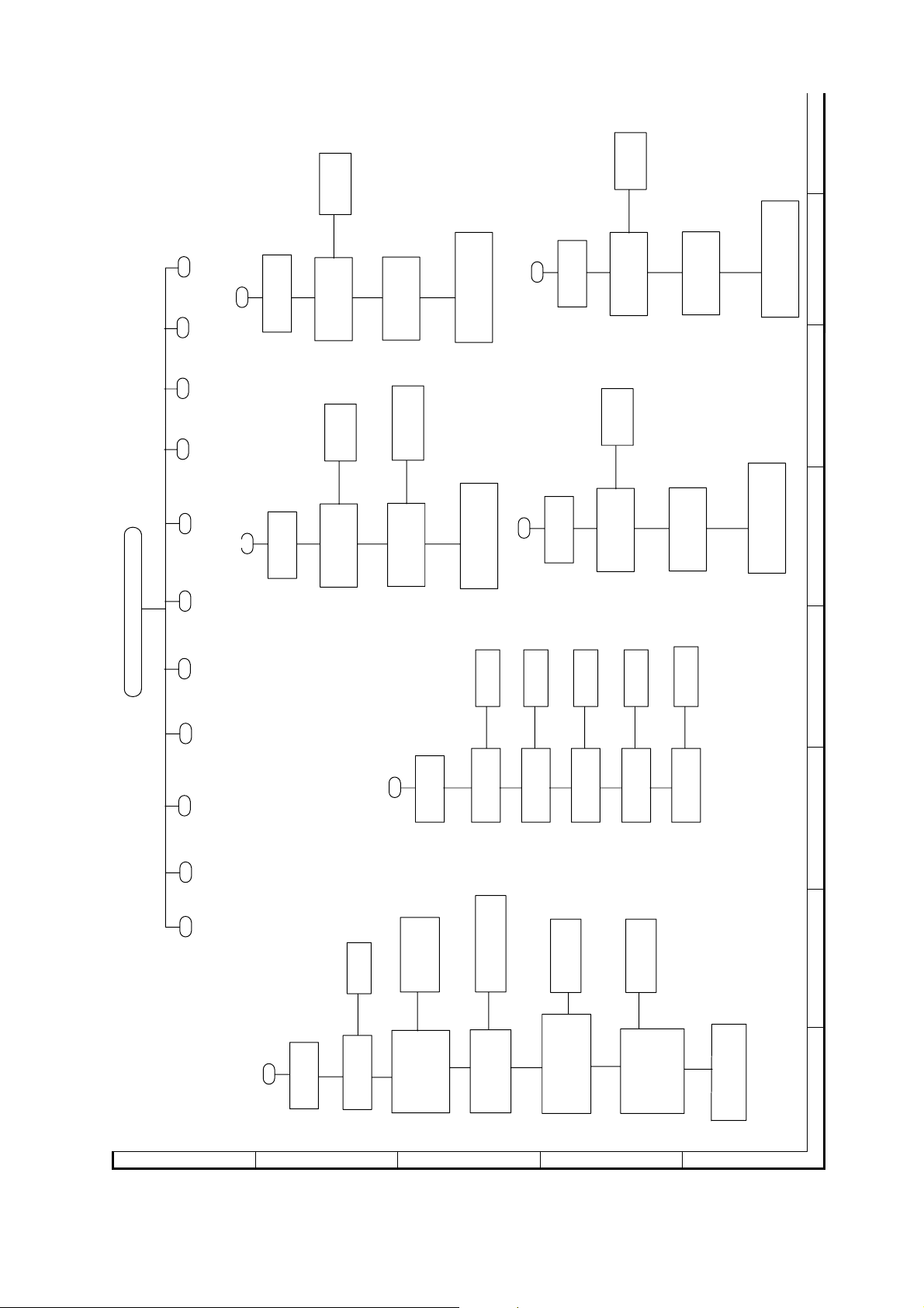
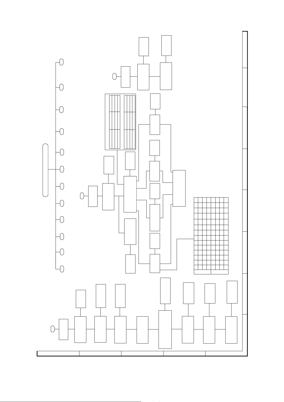
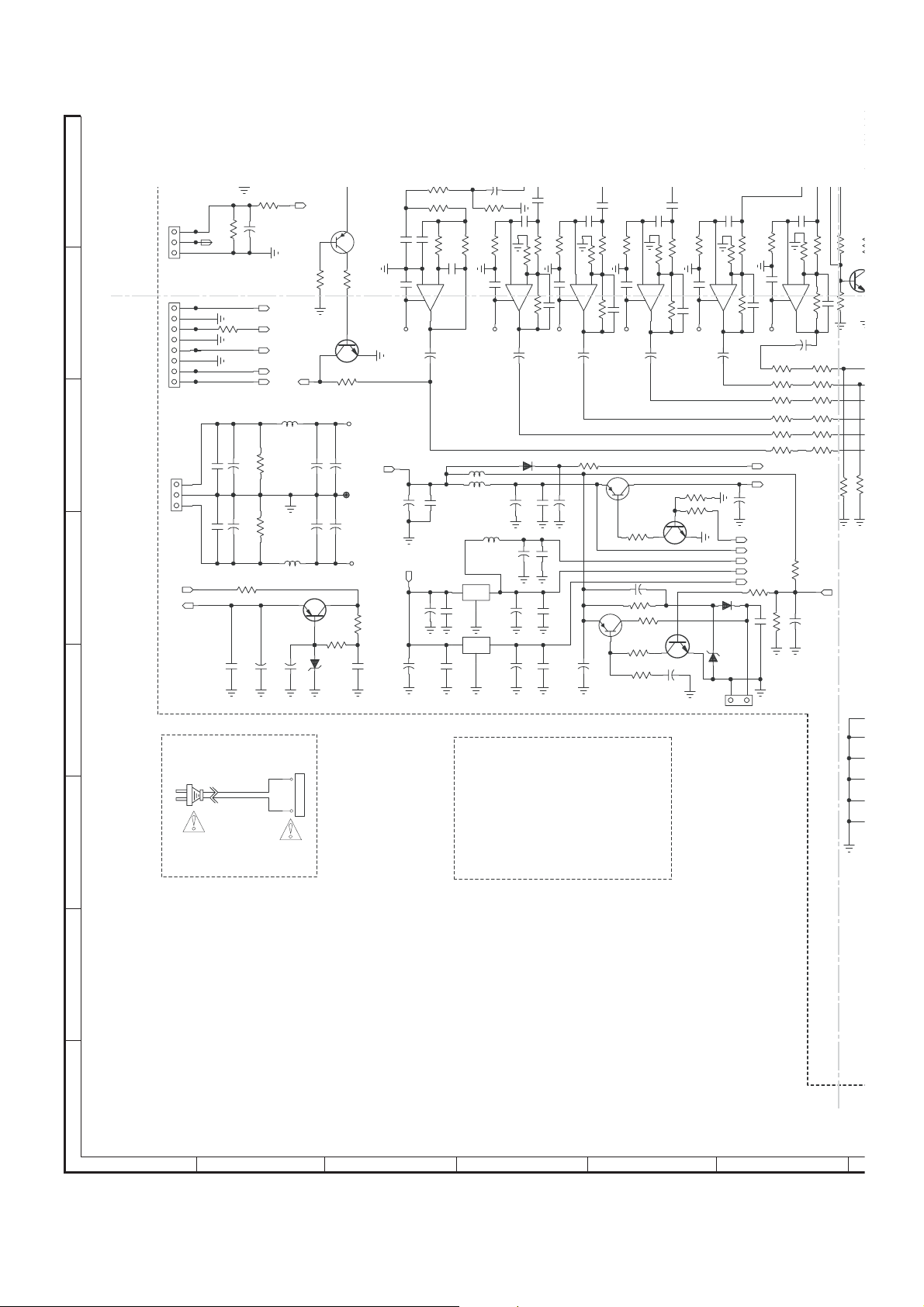
SCHEMATIC DIAGRAMS / IC’S PIN VOLTAGE
Standard Notes
WARNING
Many electrical and mechanical parts in this chassis
have special characteristics. These characteristicsoften
pass unnoticed and the protection afforded by them
cannot necessarily be obtained by using replacement
components rated for higher voltage, wattage, etc.
Replacement parts that have these special safety
characteristics are identified in this manual and its
supplements; electrical components having such
features areidentified by the mark " " in the schematic
diagram and the parts list. Before replacing any of these
components, read the parts list in this manual carefully.
The use of substitute replacement parts that do not
have the same safety characteristics as specified in the
parts list may create shock, fire, or other hazards.
Capacitor Temperature Markings
Mark
(B)
(F)
(SR)
(Z)
Capacity
change rate
±10%
+30 - 80%
±15%
+30 - 80%
Standard
temperature
20°C
20°C
20°C
20°C
Temperature
range
-25~+85°C
-25~+85°C
-25~+85°C
-10~+70°C
Notes:
1. Do not use the part number shown on these drawings for ordering. The correct part number is shown
in the parts list, and may be slightly different or
amended since these drawings were prepared.
2. All resistance values are indicated in ohms (K=10
3. Resistor wattages are 1/4W or 1/6W unless other-
4. All capacitance values are indicated in µF
5. All voltages are DC voltages unless otherwise speci-
6. Electrical parts such as capacitors, connectors, di-
6
).
M=10
wise specified.
-6
(P=10
fied.
odes, IC's, transistors, resistors, switches, and fuses
are identified by four digits. The first two digits are
not shown for each component. In each block of the
diagram, there is a note such as shown below to
indicate these abbreviated two digits.
µF).
3
,
Capacitors and transistors are represented by the
following symbols.
CBA Symbols
(Top View) (Bottom View)
+
Electrolytic Capacitor
(Top View)
Transistor Transistor
ECB
(Top View)
ECB
18
Page 19

HT-CN150DVW
LIST OF CAUTION, NOTES, AND SYMBOLS USED IN THE SCHEMATIC
DIAGRAMS ON THE FOLLOWING PAGES:
1.CAUTION:
FOR CONTINUED PROTECTION AGAINST FIRE HAZARD, REPLACE ONLY WITH THE
SAME TYPE FUSE.
2.CAUTION:
Fixed Voltage (or Auto voltage selectable) power supply circuit is used in this unit.
If Main Fuse (F1001) is blown, first check to see that all components in the power supply circuit are not defective
before you connect the AC plug to the AC power supply. Otherwise it may cause some components in the power
supply circuit to fail.
3.Note:
(1)Do not use the part number shown on the drawings for ordering. The correct pa rt number is shown in the part s list,
and may be slightly different or amended since the drawings were prepared.
(2)To maintain original function and reliability of repaired units, use only original replacement parts which are listed
with their part numbers in the parts list section of the service manual.
19
Page 20
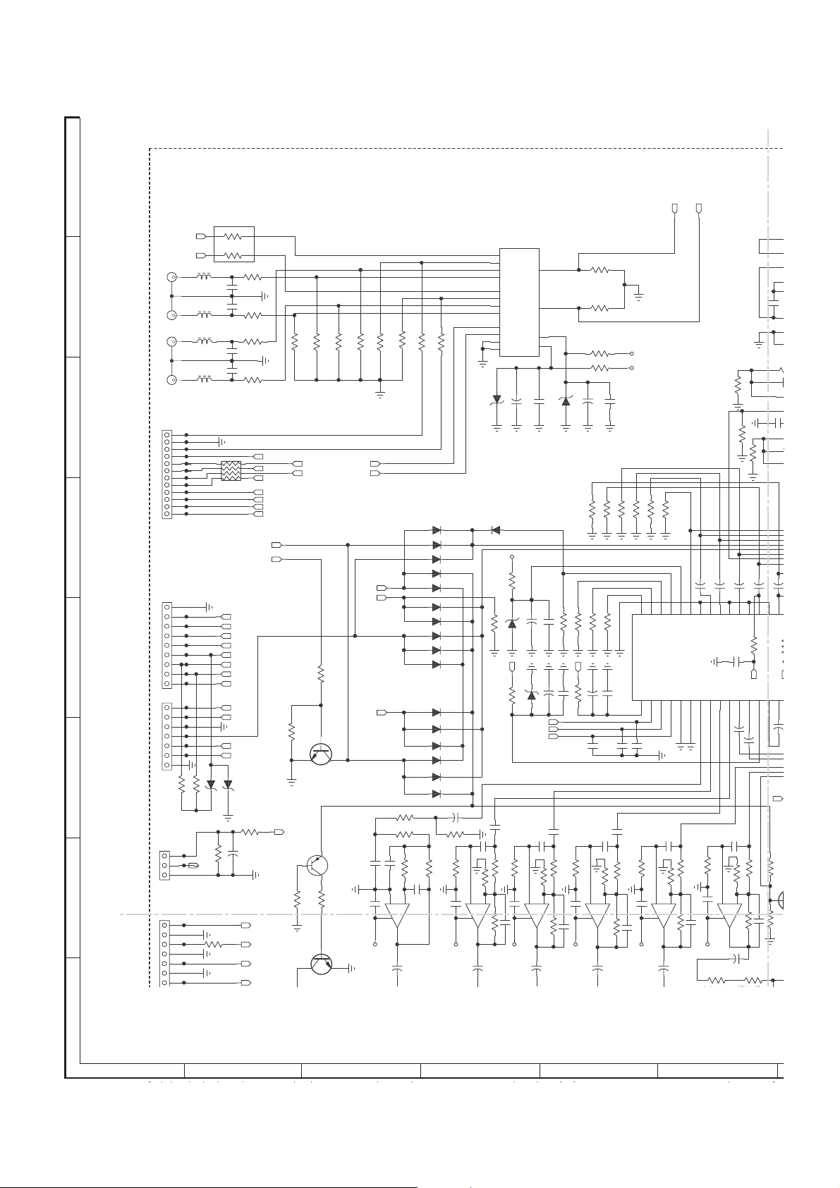
HT-CN150DVW
(
)
C449 4u7
5
4
5
R
R
R
R
R423 100K(33K)
MAIN CIRCUIT DIAGRAM
A
R323 47K
AIL
R324 47K
AIR
JK401-A
L
L301 100ohm
B
R
L302 100ohm
L
L303 100ohm
AUX IN TV IN
R
L304 100ohm
JK401-B
C
CN151 FOR TUNER PCB
1
LEFT
2
GND
3
RIGHT
4
TVCC
ENABL
5
6
DATA
7
CLOCK
8
STEREO
9
10
SCI
11
SDA
12
DAVN
D
FOR RB201
CN201
1
2
3
4
5
6
E
F
7
8
9
FOR RB202
CN202
470
470R261
R260
15V
CN903 FOR SWITCH POWER PCB
G
CN902 FOR SWITCH POWER PCB
1
2
3
4
5
6
7
8
H
+27V
1
C951 104
R301 43K
C301
100P
C302
100P
R302 43K
R303 43K
C303
100P
C304
100P
R304 43K
TVCC
5
4
3
6
2
1
RA301 33x4
ZD202 3V3
22k
R966
R968
1 1/2W
TUN-DATA
7
8
TUN-ST
+5V
SCL_RDS
SDA_RDS
DAVN_RDS
BMUTE
T5V
VFD-CE
VFD-CLK
VFD-DATE
+5V
-24V
AC1
AC2
IR
EN2(OPEN)
EN1(OPEN)
ST
T5V
24V
ZD203
R967
10K
C984
100u/25
+6VB
+12V
-24V
AC1
AC2
SUB
L951 100
470u/50
C955
23456
100u/50
R951 10K
R305 100K
ST
2SA733(OPEN)
R465 10k(OPEN)
C957
R306 100K
TUN-CLK 4052-B
R322 6KB
Q404
C
Q405 2SC945(OPEN)
R467 3K3(OPEN)
R321 47K
Q301
2SC945
B
B
VDDP
C959
470u/50
R307 100K
R466 10k(OPEN)
E
R308 100K
4052-ATUN-CE
AMUTE
E-D(SW)
MUTE
104
C494
+12V
R309 100K
C491 124
R310 100K
1N4148(OPEN)
R463 27K
R464 27K
C492 124K
5
+
B+
B
D
7
R312 10
R311 10
D316 1N4148
D301 1N4148
D302 1N4148
D305 (OPEN)1N4148
D304 1N4148
D305 1N4148(OPEN)
D306 1N4148
D307
D308 1N4148
D309 1N4148
D310 1N4148
D311 1N4148(OPEN)
D312 1N4148
D313 1N4148
D314 1N4148(OPEN)
D315 1N4148
C497
R461 390K
R462 22K
C493
6
104
102
C469
-
IC409-B
JRC4558d
C495
10u/16V
L956 100uH
R470 100K
1N4148 D317
10u/16V
C488563
R460 33K
4.7K
R4010
3
+
B-
4
D
1
IC409-A
JRC4558d
D951 1N4148
12
X0
14
15
11
1
5
2
4
10
9
6
8
ZD301 5V6
R3 0
2
-
R4005
4.7K
C490
10u/16V
IC301 TC4052B
X1
X-COM
X2
X3
Y0
Y1
Y2
Y-CO M
Y3
A
B
INH
VSS
C311 100u/16
P+12V
R424 220
ZD402 5V6
R429 220 P-12V
M62446-CLK
M62446-DATA
M62446-CE
C487 473
R458 33K
R459 15K
C484104
C4011 151
P-12VP-12VP-12V
VDD
VEE
ZD401 5V6
C453 47u/16
C482
563
4.7K
R4009
5
+
B+
B
D
7
IC409-B
JRC4558d
R953 10K
C312 104
ZD302 5V6
R425 22K
C454 104
C455 47u/16
C456 104
C480 473
R456 15K
6
-
R4004
4.7K
C486
10u/16V
R315 100K
R316 100K
R319 220
R320 220
C313 100u/16
R487 100K
R426 22K
R427 22K
+5V
220
R430
C452
30P
R457 33K
C483
104
4
C4010 151
P-12V
IC409-A
47u/16
C457
C481
563
R4008
3
+
B-
D
1
JRC4558d
P+12V
P-12V
C314 104
R488 100K
R489 100K
R490 100K
R491 100K
124357891011121314
OUT3
OUT4
R428 22K
C451
30P
4.7K
2
-
C485
10u/16V
C458 104
C479 473
R455 15K
C4009 151
42
R454 33K
P+12V
DVDD
C450
30P
IC405
M62446FP
CLK
413940
C476
104
B
IC407-B
L-IN1
R-IN1
R492 100K
C439
C440
10u/16V
6
SRIN
SWIN
AVDD
OUT1
OUT2
GNDS
DATA
LATCH
DGND
AGND
SWOUT
SROUT
383635343332313029
37
C474
563
R452 15K
R453 33K
4.7K
R4007
5
+
B+
D
7
JRC4558d
R-0
-
R4002
C478
10u/16V
C475
6
4
C4008 151
4.7K
IC407-A
P-12V
L-0
C477 10u/16V
R655 110
R656 110
R657 110
R658 110
R659 110
R670 110
BMUTE
TVCC
10u/16V
SLIN
C3 33P
SLOUT
C473
563
R4006
104
3
+
1
JRC4558d
R4024 4.7K
R420 1KB(33K)
C441
10u/16V
CIN
GNDC
R1
COUT
ROUT
1uF C472
4.7K
2
-
B-
D
4.7K
R4001
R501 5K6
R502 5K6
R521 5K6
R522 5K6
R541 5K6
R542 5K6
GNDR
5.6K
MICR
LOUT
0K(10K)
R421
R432
104(OPEN)
R4023 4.7K
10u/16V
C438
RIN
AVSS
C471uF
R451 15K
C4007 151
0K(10K)
C
1
6
5
C429
R431
2
3
C
1
10u/16V
15
LIN
GNDL
R2
5.6K
MICL
CL1
CL2
28
VDDP
R561 10K(1K)
B
R571100K
10K
0K
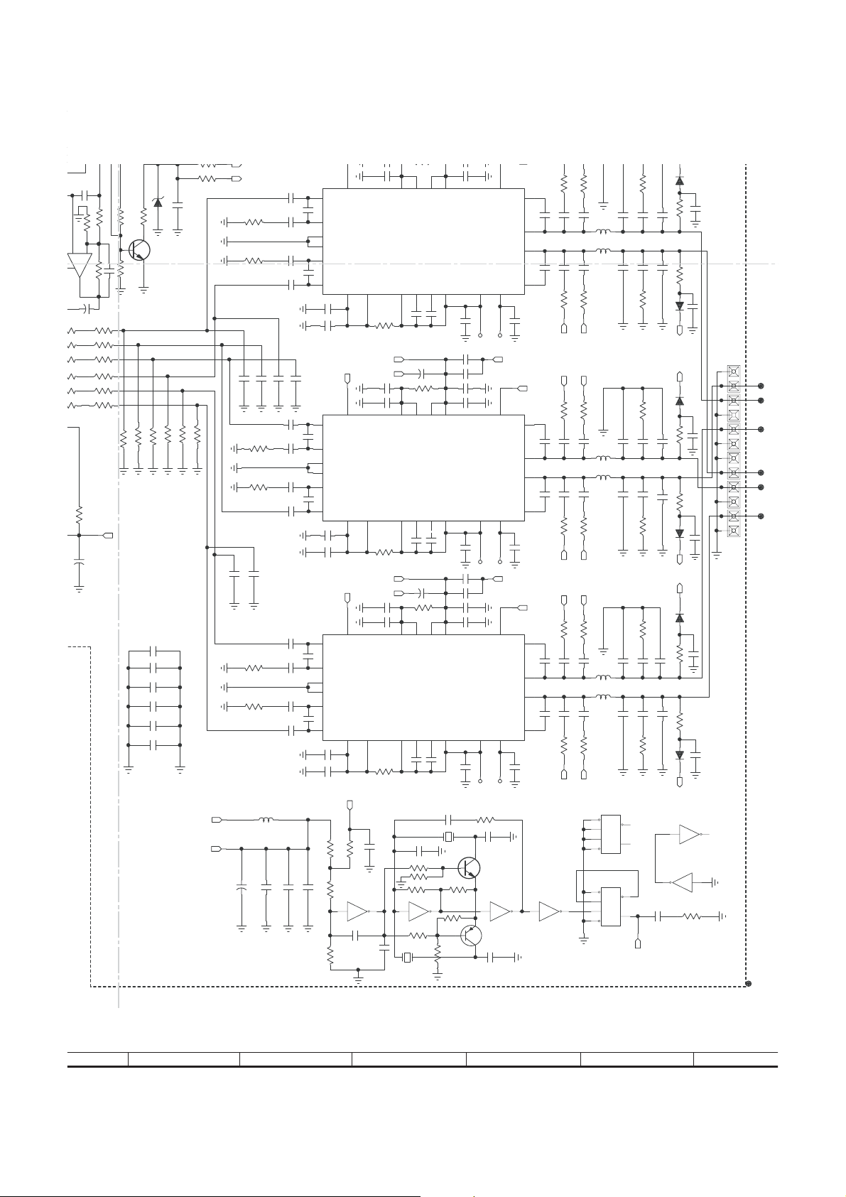
MAIN CIRCUIT DIAGRAM (1/4)
20
Page 21
R451
15K
10u/16V
C471uF
30
13
R416 1K
R417 4K7
R418 1K
R419 43K
C428
150P
IC403-B
JRC4558d
-
6
O
B+
+
8
5
C429
104 P+12V
R421 47K
R431 560P(150)
-
2
O
B-
+
IC404-A
4
3
R432
104(OPEN)
R4023 4.7K
RIN
AVSS
6V
5K6
K6
K6
K6
K6
K6
JRC4558d
R422
15K(5.6K)
C433
150
6
5
P+12V
R486
R423 100K(33K)
10K
C438
10u/16V
C437
14151617192021
GNDL
BYPASSL
BYPASSR
R2
5.6K
C4 33P
MICL LIN
CL1
CR1
CR2
CL2
29282726242322
C449 4u7
C448 4u7
VDDP
R563 39K
ZD501 5V6
R561 10K(1K)
R562 10K(330)
c
Q501
B
25C945
E
R571100K
C4007 151
100K(10K)
100K(10K)
100K(10K)
C426 10u/16V
7
11
P-12V
IC404-B
JRC4558d
-
O
B+
+
8
C435
18
LBASS3
RTRE LTRE
RBASS3
25
C507 224
7
100K(10K)
100K(10K)
7
104(OPEN)
LBASS2
RBASS2
SUB1
47
R498 47
R497
C427
103
R4022 39K
R4021
39K
C436 0.047uF
LBASS1
RBASS1
R564 220
R565 220
R566 220
100K
SR1
SL1R1L1
C1
474747
R496
R495
C430 10u/16V
C434 0.047uF
R484
18K
C442 474
C445 474
47
R494
R493
R404 4K7
R407 4K7
R410 4K7
C416
103
C421
103
R485 18K
R483 18K
R482 20K
C443 153
C446 153
MODE 2
MODE 3
C505 5K6
C506 5K6
332(390)
C5053
R402 27K
R401 4K7
R403 1K
C401
103
C402
103(562)
R406 1K
C406
103
C407
103(562)
R408 27K
R409 1K
C412
C411
103(562
103
R411 27K
R412 1K
C417
103(562
R414 27K
R415 1KR413 4K7
C422
103(562
R481
20K
C444 152
C447 152
C501 474
C503
330P
C505 474
C506 474
C504
330P
C502 474
332(390)
332(390)
332(390)
C5056
C5055
C5054
C531 474
8 9 10 11 12
C533
R4 10K
ESS
8
IN1+
9
IN1-
11
SGND1
2
SGND2
5
IN2+
IN2+
4
IN2-
C515 104
C516 104
8
IN1+
C403
150P
C404 104R405 27K
C408
150P
C409 104
C413
150P
C414 104
C418
150P
C419 104
C423
150P
C424 104
R7 3.3K
D1 IN4148
R9 56K
VCC+27V
16
B
R5 10K
ZD1 7V5
MODE
VSSA2MODE
MODE2
C405
IC401-A
10u/16V
JRC4558d
-
21
O
B-
+
4
3
P-12V
C410
IC401-B
10u/16V
JRC4558d
-
67
O
B+
+
8
5
P+12V
IC402-A
C415
JRC4558d
10u/16V
-
21
O
B-
+
4
3
P-12V
IC402-B
C420
JRC4558d
10u/16V
-
67
O
B+
+
8
5
P+12V
IC403
JRC4558d
-
21
O
B-
+
4
3
P-12V
C
Q1
2SC945
E
Q2
2SA733
C5
100u/16V
R6 100k
VDDP
VSSP
C509 104
R510 10
C510 104
3
10
VDDA2
IC501
VSSD
ASSA1
12
R511 10
C537 104
C538 104
VDDP
VSSP
24
3
VDDA2
18
C517 224
R527 10
10
C425
10u/16V
C-2
R8 10K
47U/63VC508
VDDA1
TDA8921TH
STABI
47U/63VC539
VDDA1
SR-2
14
13
14
VDDP1
PROT
VDDP1
B
C511 104
C512 104
C513 104
C514 104
23
VDDP2
SBVD
19
C518 68P
C541 104
C542 104
C543 104
C544 104
23
VDDP2
R432 68K
R434 360K
R-2
R441 68K
R442 68K
R443 68K
C
E
C519 104
R431 47K
R433 360K
R435
R440 47K
Q3
2SC945
VSSP1
17
56K
VSSP
OSC
OUT2
VSSP2
20
VSSPVSSP
VSSP
7 7
OSC
C461 47P
R436 33K(56K)
-
21
O
B-
+
3
4
P-12V
C465 47P
R444 33K
-
67
O
B+
IC406-B
+
8
5
JRC4558d
C466
104
R450 10K
R479 47K
R477 4.3K(4K7)
R476 4.3K(10K)
VCC
CLOCK
15
BOOT1
16
OUT1
21
C522 153
22
BOOT2
C520 104
CLOCK
15
BOOT1
153 C521 153 C521 153
IC406-A
Jrc4558d
104
C462
P+12V
Q409
2SA733
C523 560P
C524 560P
560P
BLNK
VDDP
VDDP
VDDP
Q403
2SA733
10u/16V
R513 5.1
R514 5.1R529 5.1
10u/16V
C467
R478 100KK
RB5001
TO CN5001
C526 560P
C463
R437 4K7(330)
Q401 CM5783
Ec
Ec
R4454K7(330)
R474
2.2K(47K)
R474
2.2K(47K)
R476 1K D318 1N4148
1
2
3
4
VSSP
R515 5.1
C525 560P
L501 27uH
L502 27uH
R516 5.1
VSSP
VSSP
R531 5.1
560P
R438
15K(3.3K)
B
B
Q402
CM5783
R446
15K(3.3K)
R472 47K(3.3K)
R471 47K(3.3K)
R449 1K
R448 1K
Q407
2SC945
Q408
2SC945
CE C
BB
E
R468
12K(OPEN)
SUB
R517 22
224
C529
C530 224
C528 M1uF
C5062 103
R518 22
D506
R533 22
224
103
M1uF C527 M1uF
MAIN CIRCUIT DIAGRAM (2/4)
R439 47K
L306 100ohm
L305 100ohm
R447 47K
R471 47K(3.3K)
R4011 47K
R4012 47K
7
6
3
2
4
5
1
R469
47K(OPEN)
D504
R519 10K
C5061 103
1N4148
C5095 103 R520
F_AF_A F_A
D501 1N4148
10K
HT-CN150DVW
C464 470P(100P)
JK401-C
L
LINE OUT
R
C468470P(100P)
AOL
C4001 470P
AOR
C4002 470P
JK5001
CN401
OPEN
1
2
C496104(OPEN)
1N4148
C5094 103
10K
12
11
10
9
8
103
C5096
R
L
C
21
Page 22
HT-CN150DVW
7
7
M62446-DATA
7
7
7
7
7
A
B
C
D
E
F
470
470R261
R260
ZD202 3V3
22k
15V
R966
CN903 FOR SWITCH POWER PCB
CN902 FOR SWITCH POWER PCB
1
2
3
4
5
6
7
8
R968
1 1/2W
+27V-27V
C951 104C952 104
1
2
3
CN901
FOR SWITCH POWER PCB
C969
104
R957 180 1W
-24V
P-12V
ST
T5V
24V
ZD203
R967
10K
C984
100u/25
+6VB
+12V
-24V
AC1
AC2
L951 100
C955
100u/50
R951 10KR952 10K
C956
100u/50
L952 100
2SA952
C970
100u/25
100u/25
TO SWITCH POWER PCB
SUB
Q953
C971
470u/50
470u/50
C957
C958
ST
2SA733(OPEN)
R465 10k(OPEN)
EBC
Q301
2SC945
B
R322
Q404
B
C
Q405 2SC945(OPEN)
R467 3K3(OPEN)
C959
470u/50
C960
470u/50
R958 330
ZD951 12V
R466 10k(OPEN)
VDDP
TP951
VSSP
1uF C472
C473
563
4.7K
R4006
C475
104
3
2
-
+
B-
4
D
1
4.7K
R4001
IC407-A
JRC4558d
L-0
C477 10u/16V
R501 5K6
R502 5K6
R521 5K6
R522 5K6
R541 5K6
R542 5K6
R970
1M(OPEN)
R965 OPEN(51K)
C983 10u/16V
C4
VDDP
R451 15K
B
C4007 151
R503 100K(10K)
R544 100K(10K)
C449
R561 10K(1K)
R562 10K(330)
R571100K
R504 100K(10K)
C50
C50
C50
C50
C50
C50
C964
104
2
-
R4005
4.7K
C490
10u/16V
C487 473
R459 15K
P-12VP-12VP-12V
C968
104
C976
104
C980
104
C4011 151
M62446-CE
C482
563
R458 33K
4.7K
R4009
C484104
5
+
B+
B
D
7
IC409-B
JRC4558d
R953 10K
C965 220u/25
C981 220u/16
6
-
R4004
4.7K
C486
10u/16V
2SA952
C480 473
R456 15K
C4010 151
P-12V
2SA952
C985 470u/16
R960 390 1/2W
C452
30P
C481
563
R457 33K
R4008
C483
104
3
+
B-
4
D
1
IC409-A
JRC4558d
Q951
2SC945
R954 4K7
R961 22 1/2W
R962Q954
2K2 (1.5K)
R988 2K2(OPEN)
10u/16V(OPEN)
C451
4.7K
C485
10u/16V
Q952
30P
-
C988
R455 15K
2
R955 100K
B
CBE
30P
C479 473
R454 33K
C4009 151
P+12V
R956 10K
EC
Q955
2SC945
C450
C474
563
R4007
C476
104
5
+
B+
B
7
IC407-B
JRC4558d
D960 OPEN(0)
CN908
4.7K
-
D
R4002
C478
10u/16V
R-0
Tun_B+/SW
ZD952
7V(OPEN)
2
R452 15K
R453 33K
6
C4008 151
4.7K
P-12V
R655 110
R656 110
R657 110
R658 110
R659 110
R670 110
BMUTE
TVCC
C966
220u/16
P+12V
+M5V
+5V
VCC
R963 0
104
C982
1
D312 1N4148
D313 1N4148
D314 1N4148(OPEN)
D315 1N4148
R463 27K
R464 27K
R462 22K
C492 124K
C491 124
C493
6
5
104
C494
E
+12V
C961
100u/16
R959
220
C972
104
+6VB
C973
B
220u/25
C977
+
B+
7
220u/25
-
D
IC409-B
C495
10u/16V
104C902
102
JRC4558d
L956 100uH
C974
104
C978
104
L955 100uH
IC953
1
BA05T
1
IC954
BA05T
10u/16V
C497
R470 100K
R461 390K
R460 33K
104
C469
C963
470u/16v
L957 100uH(10uH)
C967
220u/16v
3
2
C975
220u/10v
3
2
C979
220u/10v
C488563
4.7K
R4010
3
+
B-
4
D
1
IC409-A
JRC4558d
D951 1N4148
SWITCH POWER
G
H
1
23456
MAIN CIRCUIT DIAGRAM (3/4)
22
Page 23
0
5
IC407-A
2
4
4
HT-CN150DVW
100u/
ZD1
VDDP
VSSP
C509 104
C510 104
MODE
IC501
ASSA1
VSSA2MODE MODE
12
R511 10
VDDP
MODE2
VSSP
C537 104
C538 104
IC502
ASSA1
VSSA2
12
R528 10
VDDP
MODE3
VSSP
C577 104
C578 104
IC503
ASSA1
VSSA2
12
R548 10
C5045 102
R5043 1K
C5060
100P
C
R6 1
47U/63VC508
R510 10
3
14
10
VDDA2
VDDA1
VDDP1
TDA8921TH
VSSD
PROT
STABI
13
18
24
C517 224C586 224
47U/63VC539
R527 10
14
10
VDDA2
VDDA1
VDDP1
TDA8921TH
VSSDVDDA2
PROT
STABI
13
18
24
C547 224
47U/63VC579
R547 10
14
10
VDDA1
VDDP1
TDA8921TH
VSSD
STABI
PROT
13
18
24 3 3
C5047 33P
CF5041 C5048
600KHz
C5049 100P
R5045 47K
R5052 OPEN
R5046 1M
IC504-C
74HCO4
R5048 47K
CF5042
700KHz
C511 104
C512 104
C513 104
C514 104
23
VDDP2
SBVD
19
C518 68P
C541 104
C542 104
C543 104
C544 104
23
VDDP2
SBVD
19
C580 104
C581 104
C582 104
C583 104
VDDP2
SBVD
19 23
C587 68P C548 68P
2SC945
B
R5047 6K
R5051
10K
47K
R5062
IC504-B
74HCO4
C549 104 C519 104
C588 104
Q5041
VSSP1
17
VSSP1
17
VSSP
VSSP1
17
VSSP
R5044 10K
C
E
Q5042
25A733
C5050 100P
20
VSSPVSSP
VSSP
7
20 20
VSSP
100P
IC504-B
74HCO4
7 7
VSSP
OSC
VSSP2
VSSP
OSC
VSSP2
VSSP
OSC
VSSP2
OUT1
OUT2
OUT1
OUT2
OUT1
OUT2
CLOCK
15
BOOT1
16
21
22
BOOT2
CLOCK
15
BOOT1
16
21
22
22
C560 104 C520 104
CLOCK
15
16
21
22
BOOT2 BOOT1 BOOT2
C589 104
C522 153
C561 153 C521 153 C521 153
C562 153
C590 153
C595 153
IC504-E
74HCO4
VDDP
R513 5.1
C523 560P
C524 560P
R514 5.1R529 5.1
VDDP
VDDP
C563 560P
C564 560P
R530 5.1
VDDP
VDDP
R549 5.1
C591 560P
C596 560P
R553 5.1
VDDP
VSSP
R515 5.1
C525 560P
L501 27uH
L502 27uH
C526 560P
R516 5.1
VSSP
VSSP
R531 5.1
C565 560P
L503 27uH
L504 27uH
C566 560P
VSSP
R550 5.1 R532 5.1
C592 560P
L505 27uH
L506 27uH
L505 27uH
C597 560P
R554 5.1
VSSP VSSP
IC505-B
CD4013BM
8
9
11
10
IC505-A
CD4013BM
6
5
3
4
SET
DATE
>CLK
RESET
SET
DATE
>CLK
RESET
SUB
C567 M1uF C527 M1uF
C568 M1uF C528 M1uF
C593 M1uF
C598 M1uF
12
Q
13
Q
2
Q
1
Q
CLOCK
R517 22
224
C530 224
R518 22
R533 22
224
C569 C529
C570 224
R551 22 R534 22
C599 224 C594 224
R555 22
C5051 100P
R468
12K(OPEN)
R469
47K(OPEN)
R519 10K
C5061 103
C5062 103
D506
1N4148
F_AF_A F_A
D501 1N4148
R535 10K
C5063 103
C5064 103
D503
1N4148
D505
1N4148
10K
R552
C5065 103
C5066 103
D502
1N4148
F_A F_A F_A
IC504-D 74HCO4
98
12
IC504-F 74HCO4
R5049 22
D504
1N4148
C5094 103
10K
R520
103
C5096
10K
R536
C5095 103 C5095 103
C5093 103
10K
R556
C5091
13
CN401
OPEN
1
2
C496104(OPEN)
12
11
10
9
8
7
6
5
4
3
2
1
JK501
103
PCB
R
L
C
SR
SL
SW
R451 15K
2
4.7K
R544 100K(10K)
C44C4
VDDP
R561 10K(1K)
B
R571100K
C4007 151
R503 100K(10K)
R504 100K(10K)
C5071 104
C5072
C5073
C5074
C5075
C5076
R563 39K
ZD501 5V6
R562 10K(330)
c
Q501
25C945
E
R524 100K(10K)
R523 100K(10K)
104
104
104
104
104
R564 220
R565 220
R566 220
C507 224
R543 100K(10K)
R544 100K
TO-IC504-IC505
R9 56K
VCC+27V
MODE 2
MODE 3
C501 474
8
IN1+
C503
330P
C505 5K6
C505 474
C506 474
C506 5K6
C504
330P
C502 474
332(390)
332(390)
332(390)
332(390)
C5056
C5055
C5054
C5053
C531 474
C533
330P
R525 5K6
C535 474
C536 474
R526 5K6
C534
330P
C532 474
C5058 332(390)
C5057 332(390)
C571 474
C573
330P
R545 5K6
C575 474
C576 474
R546 5K6
C574
330P
C572 474
C5041 10u/16V
L959 1uH
C5042 104
C5043 104
+5V
9
IN1-
11
SGND1
2
SGND2
5
IN2+
IN2+
4
IN2-
16 6
C515 104
C516 104
8
IN1+
9
IN1-
11
SGND1
2
SGND2
5
IN2+
IN2+
4
IN2-
1
C545 104
C546 104
8
IN1+
9
IN1-
11
SGND1
2
SGND2
5
IN2+
IN2+
4
IN2-
1
C584 104
C585 104
FERQ_HOP
R5041 10K
R5042 1K
C5044 104
12 56 3 41110
1uF C47
C473
563
4.7K
R4006
104
3
-
+
B-
D
1
R4001
JRC4558d
L-0
477 10u/16V
R501 5K6
110
R502 5K6
110
110
R521 5K6
R522 5K6
110
110
R541 5K6
R542 5K6
110
R970
1M(OPEN)
R965 OPEN(51K)
C983 10u/16V
IC504-A 74HCO4
C5046
470P
R5053
470K
6
7
8 9 10 11 12
MAIN CIRCUIT DIAGRAM (4/4)
23
Page 24
HT-CN150DVW
R
0
R
3
7
1
9
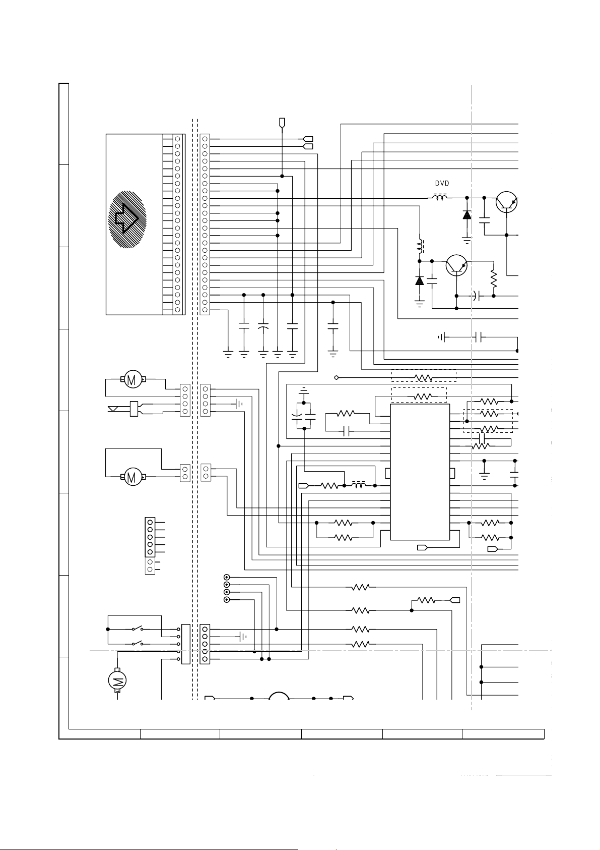
SERVO CIRCUIT DIAGRAM
A
B
C
DVD LOADER (AMTEK)
DVD PACK
CN801
1
TRACK- IC802 20PIN
2
TRACK+ IC802 15PIN
3
FOCUS- IC802 5PIN
4
FOCUS+ IC802 14PIN
DVDPD IC801 23P
5
RF50V VCC5V
6
GND
7
8
GND
9
DVDLD
10
CDLD
11
GND
GND
12
CDPD IC801 24P
13
GND
14
15
DVDRF C816-IC801 1#
C IC801 14# 10#
16
B IC801 11# 15#
17
A IC801 12# 16#
18
D IC801 9# 13#
19
F IC801 17#
20
21
E IC801 18#
RF50V
22
PVC
23
24
GND
104
C804
IC801 20#
C801
100u/16
RF50V
104C802
TRACKTRACK+
104
C803
L802
VCD/CD
1UH
L801
1.8V
1N4148
D801
102C805
Q805
1UH
3.9V
2.1V
1N4148D802
2SB1132
104
C805
4.5V
100u/16
C807102
C809
Q806
R804 10
3.9V
2SB1132
RF50V
C808
4.6V
100u/16
R805 10
SP MOTOR
D
E
SLED MOTOR
SW803
SW804
M44
CN2
CN3
TRAY-SW1
TRAY-SW2
F
G
RB813
CN813
1
1
2
3
4
RB812
2
1
1
-12
2
+12
3
EN2
4
EN1
5
GND
2
MICL
1
MICR
RB803
1
2
3
4
5
2
3
4
CLOSE(189PIN)
CN812
2
1
TP36
TP35
TP34
TP33
CN803
1
2
3
4
5
VCC
SP+OUT
SP-OUT
SLED+OUT
CLOSE SW
OPEN SW
DCLOADDCLOAD+
SLED-OUT
Q201
KST2222(OPEN)
H
220u/16
C967
+12V
104
C968
MVCC
R969
15 1/2W
R813
R814
CLOSE
R871
47K
L803
SLED-OUT
SLED-OUT
R815 1K
R816
C871
FOCUSCLOSE
1
1
R817
R818
VCC33V
100P
OPEN
1UH
1K
1
2
3
4
5
6
7
8
9
10
11
12
13
14
CLOSE(189PIN)
OPEN(191PIN)
0
CLOSEW(187PIN)
0
OPENSW(190PIN)
R808
R810
FOCUS IN
CAP1-1
CAP1-2
SLED IN
FOCUS - OUT
CLOSE IN
OPEN IN
VCC5V
OPEN OUT
CLOSE OUT
SLED- OUT
SLED+ OUT
FOCUS- OUT
FOCUS+ OUT
TRACK+
R270
IC802
AM5660
39K
MUTE
BIAS
TRACK IN
CAP4 -1
CAP4 -2
SP IN
GND
MVCC5V
TR- OUT
MVCC5V
SP- OUT
SP+ OUT
TR- OUT
TR+ OUT
4.7K
OPEN
28
27
26
25
24
23
22
21
20
19
18
17
16
15
RF33V
C870
R873
R834
R819
R821
TRACK-
R831
R832
100P
47K
OPEN
10K
1
1
39K
D80
VREF IN
C872
104
R812
5V
LM358
IC805-A
R811
100u/16
1
20
4
0
4K
C834
3.3V
OPEN/CLOSE
MOTOR
1
C269
23456
R252 150(OPEN)
ZD201
104
4V6(OPEN)
C270
100u/16
TUN_B+/SW
MUTE
R24
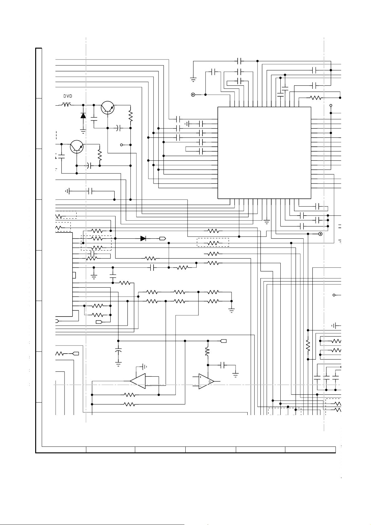
SERVO CIRCUIT DIAGRAM (1/8)
24
Page 25
C
2
2
Q
A
B
C
R808
R810
D
1
FOCUS IN
2
CAP1-1
3
CAP1-2
4
SLED IN
5
FOCUS - OUT
6
CLOSE IN
7
OPEN IN
E
8
VCC5V
9
OPEN OUT
10
CLOSE OUT
11
SLED- OUT
12
SLED+ OUT
13
FOCUS- OUT
14
FOCUS+ OUT
TRACK+
F
LOSE(189PIN)
PEN(191PIN)
LOSEW(187PIN)
G
PENSW(190PIN)
H
L802
VCD/CD
1UH
L801
1.8V
1N4148
D801
TRACK IN
CAP4 -2
IC802
AM5660
MVCC5V
TR- OUT
SP- OUT
SP+ OUT
TR- OUT
TR+ OUT
R270
Q805
102
C805
39K
MUTE
BIAS
CAP4 -1
SP IN
GND
MVCC5V
4.7K
1UH
3.9V
OPEN
28
27
26
25
24
23
22
21
20
19
18
17
16
15
RF33V
2.1V
1N4148D802
2SB1132
104
R821
C870
R873
TRACK-
C805
R834
R819
C807102
4.5V
100u/16
C809
R831
R832
Q806
R804 10
3.9V
100P
47K
OPEN
10K
1
1
2SB1132
39K
3.3V
RF50V
C834
C808
R812
100u/16
IC805-A
4.6V
VREF IN
C872
104
5V
LM358
R811
R805 10
D803
100u/16
1
R823
R833
200 1/4W
4
B-
0
1M
4K7
C833
R825
R830
1N4148
3
2
3.3V
10K
1K
104
10K
C816
680P(OPEN)
C814
C812
680P(OPEN)
RESET#
R835
R829
3.3V
R826
1K5 (0)
472
TP1
OPEN
1K5
C815
C813
680P
C811
680P
C810
HT-CN150DVW
1UF
C818
820P(104)
C817
1
DVDFRP
104
2
DVDRFN
3
A2
4
B2
5
C2
6
D2
7
CP
100P
8
CN
9
D
10
C
11
B
12
A
13
CD_D 15PIN
14
CD_C
15
CD_B 13PIN
16
CD_A
0(15K)
R809
R820
R822
R824
5
6
B+
L830 1UH
R827
R828
5V
8
LM358
IC805-B
C873
10K
0(15K)
22K
22K
7
104
C819
C820
104
C822
470P
646362616059585756555453525150
API
RFDC
RFSIN
ATOP
ATON
AIN
VPA
RFAC
BYP
DIP
DIN
IC801 ES6603S
CD_F
CD_E
VPBVCDVDLD
CDLD
DVDPD
CDPD
VNB
LDON
MIRRMPMB
171819202122232425262728293031
MIRR
SLDC
0
MVCC
104
C228
473
C227
FNP
C823
470P
FNN
VNA
MEV
MLPF
MIN
C829
C831
C230
152P
C229
473
49
RX
SDATA
MEVO
32
152P
C821
C824
R806
SDEN
SCLK
V33
LCP
LCN
MNTR
V25
V125
TPH
DFT
LINK
150P
103
CE
FE
TE
PI
C830
R208
224
33K
C231
MIRR
1UF
104
103
12K
RF33V
C8
48
SCSJ
47
SDATA
46
SCLK
45
44
43
42
41
40
39
38
37
36
35
34
33
104
C223
CEI
FEI
TEI
SBAD
C828
333
TP5
RF33V
R209
R210
47P
C224
R213
R215
C826
C8
104
C225
C232
C259
2
5
6
C260
30P
30P
Q0
Q1
3
D0
4
D1
7
2
LD0
LD1
LD2
TUN_B+/SW
1
MUTE
FERQ_HOP
TUN-CLK
TUN-CE
23456
R249
R250
R251
33
33
33
33P
C233
33P
C234
33P
R
C235
R2
SERVO CIRCUIT DIAGRAM (2/8)
25
Page 26
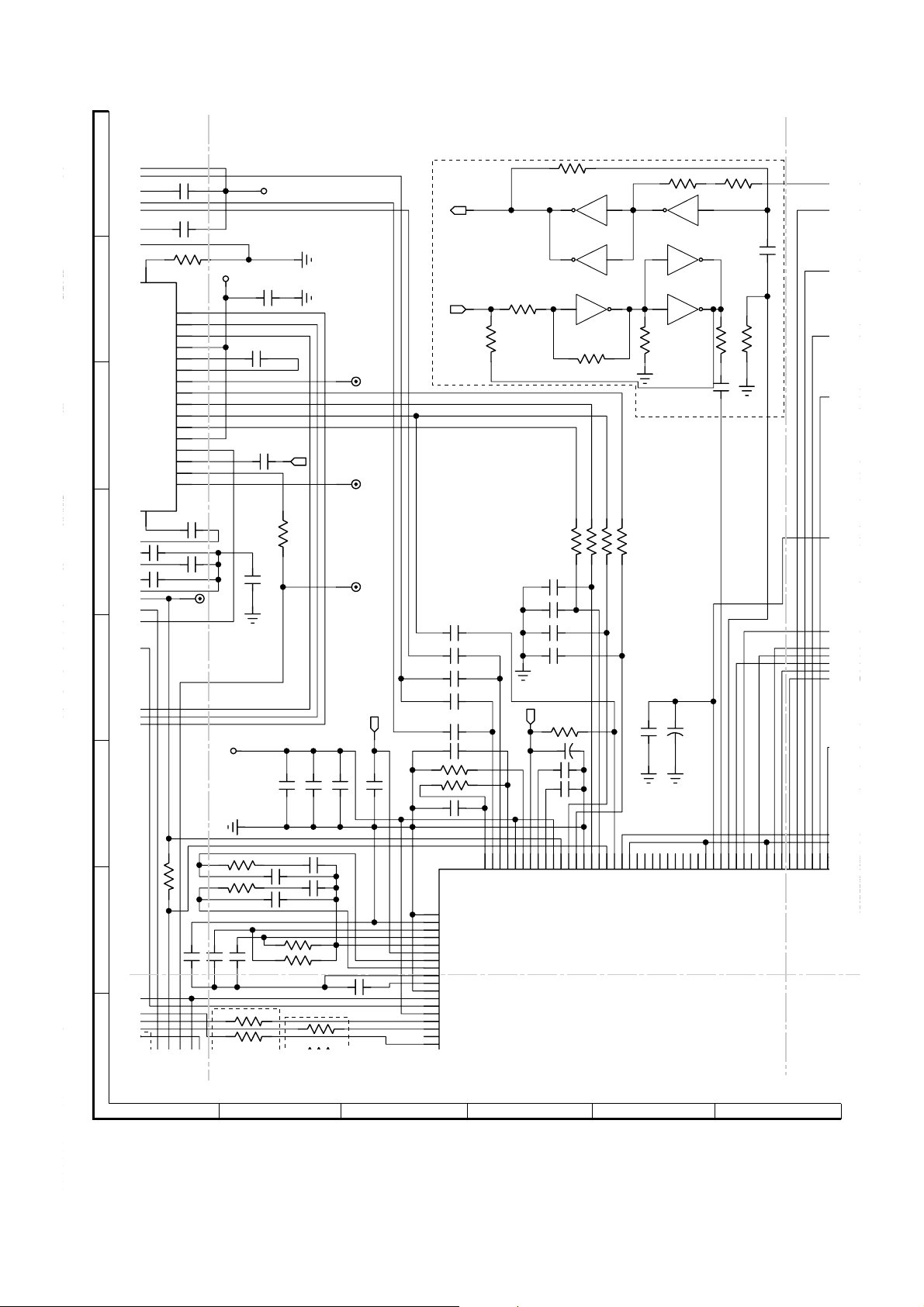
HT-CN150DVW
106
YUV3/COMP
56
BYP
25
VNB
(
)
IC803-B
74HCO4
R850
10K(OPEN)
IC803-D
74HCO4
IC803-C
74HCO4
R847
9
6
4
10u/50
C289
10M(OPEN)
10(OPEN)R851
104(OPEN)
C258
TBCK
C257
1uF(0.22uF)
MCLK
4K7
R247
TSD2
TSD1
TSD0
L823 1uH
OPEN
7V5
TWS
R848
R845
100(OPEN)
C201
C202
C203
C204
SVREF15
C206
C207
C205
A
C823
470P
C822
470P
55545352515049
DIP
DIN
FNP
FNN
VNA
MEV
B
C
LDON
MIRRMPMB
MLPF
MIN
26272829303132
C829
MIRR
SLDC
D
C831
E
F
R806
RX
SDEN
SDATA
SCLK
MNTR
V125
MEVO
C821
C824
V33
LCP
LCN
V25
TPH
DFT
LINK
150P
103
CE
FE
TE
C830
104
103
12K
RF33V
48
SCSJ
47
SDATA
46
SCLK
45
44
43
42
41
CEI
40
FEI
39
TEI
38
SBAD
PI
37
36
35
34
33
C828
224
333
TP5
MIRR
RF33V
C826
C825
C827
473
C832
104
RF50V
104
104
RF50V
104
C218
0
R807
104
C217
104
C216
TP2
TP4
TP3
PLL33V
104
C215
C208
C209
C210
C211
C212
C213
R206
R207
C214
SPDIF-OUT
IC803(OPEN)
SPDIF-IN
R888
0(OPEN)
104
472
OPEN
OPEN
472
OPEN
68K
20K
682
R205
10
12
IC803-A
74HCO4
102
102
102
102
0
IC803-E
74HCO4
IC803-F
74HCO4
1
R849 10K(OPEN)
3K3
3K3
R203
R204
10K
4u7
1UF
1UF
3K3
R202
R846
1M(OPEN)
11
8
13
5
3
2
3K3
R201
104
C290
C227
33K
R209
R210
R208
G
C230
152P
C229
473
C228
473
H
33P
33P
C235
C234
152P
104
C223
C231
1UF
1
47P
C224
R213
R215
C232
104
C225
C222
R221
OPEN
C220
1K2
15K(0)
153
R211
0
OPEN
C219
OPEN
C221
473
560P
10K
R212 5K1
SVREF15
R214
R216
R217
R218
R219
R220
C226
0
0
6K8
33
33
33
104
23456
33
CLOSE(189PIN)
XSCSJ
XSDATA
XSCLK
SDEFCT
SLDC
SPDON
157
158
159
160
161
162
163
164
165
166
167
168
169
170
171
172
173
174
175
176
177
178
179
180
181
182
183
184
185
186
187
188
189
190
191
192
193
AVSS-DS
AVSS-PL
XSPDOFTR1
XSFD0
XSFTR0PI
AVDD3-PL
XSPLLFTR1
XSPLLFTR2
XSERVF0
XSAWRC
AVSS_DA
XSRFRPCTR
XSTRAY
AVDD3_DA
XSSPINDLE
XSFOCUS
XSSLEGP
XSSLEGN
XSTRACK
XSTESTDA
XSFGIN
XSPHOI
XSCSJ
XSDATA
XSCLK
XSDFCT
XSLDC
XSSPDONG
VDD33
VSS33
XGPIO(9)
XGPIO(8)
XGPIO(7)
XGPIO(6)
XGPIO(5)
XGPIO(4)
156
155
154
XSRFIP
XSDSSLV
153
152
XSIPIN
XSRFIN
151
150
149
XSIREF
AVDD3_DS
XSVREF[09]
XSVREF[15]
148
147
146
XSRFRP
AVDD3_AD
XSVREF[21]
145
XSTEI
144
XSCEI
143
142
141
140
XSFEI
XSSBAD
AVSS_AD
139
138
137
136
135
134
133
132
131
VSS
VDD
XSIP1
XSFLAG[0]
XSFLAG[1]
XSFLAG[2]
XSFLAG[3]
XSIP2
XSTEXI
XSTESTAD
IC201 ESS6629FD
130
XSLG
129
128
127
VS33
XSWBL
XSWBLCLK
126
125
124
123
VD33
TBCK3
SPDIFIN
SPDIF/SEL_PLL3
122
MCLK
121
120
TSD3
119
TSD2
VS33
118
117
116
115
TWS/SEL_PLL2
TSD1/SEL_PLL1
TSD0/SEL_PLL0
114
113
112
111
VS33_DA
YUV5/YDAC
YUV0/UDAC
YUV2/CDAC
110
109
108
VD33_DA
YUV7/FDAC
YUV6/VDAC
107
YUV4/RSET
SERVO CIRCUIT DIAGRAM (3/8)
26
Page 27
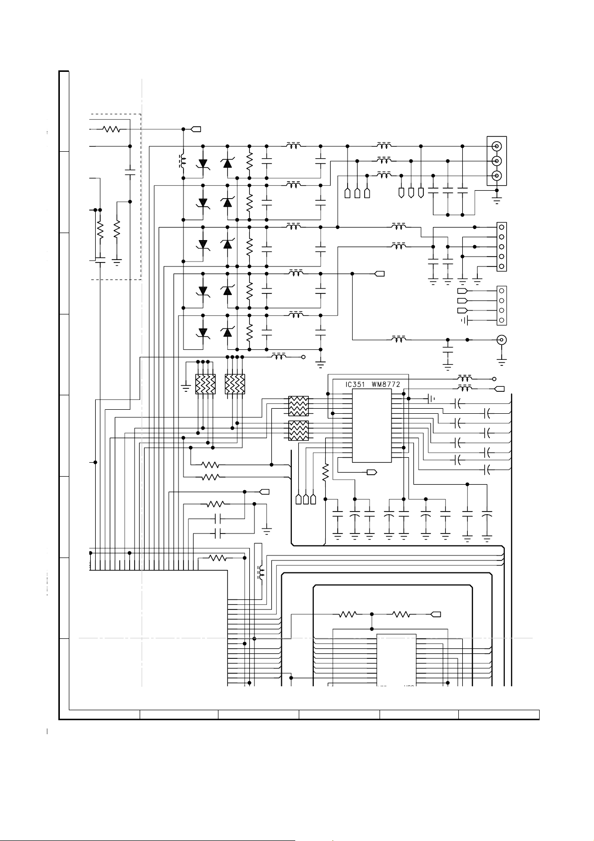
XSFLAG[3]
A
B
IC803-B
74HCO4
R850
10K(OPEN)
C
IC803-D
74HCO4
IC803-C
74HCO4
R847
10M(OPEN)
9
6
4
104(OPEN)
C258
10(OPEN)R851
R846
M(OPEN)
8
5
3
D
E
104135
C290
10u/50
C289
F
TBCK
134
133
132
131
130
129
128
127
126
125
124
VS33
VD33
XSLG
XSIP1
XSIP2
XSWBL
XSFLAG[0]
XSFLAG[1]
XSFLAG[2]
G
SPDIFIN
XSWBLCLK
SPDIF/SEL_PLL3
H
1
C201 ESS6629FD
MCLK
123
122
MCLK
TBCK3
C257
1uF(0.22uF)
4K7
R247
TSD2
121
120
TSD3
TSD2
TSD1
TSD0
TWS
119
118
117
116
115
VS33
TWS/SEL_PLL2
TSD1/SEL_PLL1
TSD0/SEL_PLL0
HT-CN150DVW
OUT
VIDEO OUT
1uH
1uH
10u/16V
C352
10u/16V
C354
10u/16V
C356
10u/16V
C358
10u/16V
104
C360
L0E#
LCS3#
LA20
LA19
LD7
LD6
LD5
LD4
LD3
LD2
LD1
LD0
V
Y
JK801
OPEN
1
3
5
6
JK802-A
1
2
3
4
5
CN804
1
2
3
4
JK802-B
6
VD33D
RWS
RBCK
RSD
7
VCC
6CH-6
6CH-5
6CH-4
6CH-3
6CH-2
6CH-1
6CH-7
6CH-8
10u/16V
C359
R854 75
VCC
L823 1uH
ZD801 7V5
ZD803 7V5
ZD805 7V5
ZD807 7V5
ZD809
7V5(OPEN)
R246 0
R245
R244
C256
C255
109
108
107
106
YUV4/RSET
YUV7/FDAC
YUV6/VDAC
YUV3/COMP
RBCK/TDMCLK
R243 0
105
VS33_PL
YUV1/VREF
VD33_PLL
RWS/TDMFS
RSD/TDMDR
LWRLL
VS33
LCS0
114
113
112
111
VS33_DA
YUV5/YDAC
YUV0/UDAC
YUV2/CDAC
110
VD33_DA
23456
ZD802 7V5
ZD804 7V5
ZD806 7V5
ZD808 7V5
ZD810
7V5(OPEN)
RN210 4K7 x4
0
390
104
104
104
103
102
101
100
LD7
99
LD6
98
LD5
97
LD4
96
VD33
95
94
LD3
93
LD2
92
LD1
91
LD0
90
LOE
89
88
CLS3
87
VDD
86
VSS
85
LCS2
84
LCS1
83
82
LA0
81
LA1
80
LA2
79
VD33
78
VS33
77
LA3
76
LA4
75
LA5
74
LA6
73
LA7
72
LA8
71
VDD
70
R852 75
R853 75
R854 75
R855 75
R865
75(OPEN)
RN209*x4
VCC33V
1UH
L202
L206
LOE#
LCS3#
LCS2#
LCS1#
L804
C844
470P
L805
C846
470P
L806
C848
470P(270)
L807
C850
470P
1uH(OPEN)
C852
470P(OPEN)
1UH
RA351
RA352
33 x4
RWS
RBCK
LD7
LD6
LD5
LD4
LD3
LD2
LD1
LDD
1uH
1uH
1uH
L808
VD33D
C845
470P
C847
470P
C849
1uH
C851
470P
33 x4
WM8772-CE
WM8772-CLK
LA0
LA1
LA2
LA3
LA4
LA5
LA6
LA7
LA8
470P(220)
C853
470P(OPEN)
33
R351
WM8772-DATA
RSD
LA16
LA15
LA14
LA13
LA12
LA11
LA9
LA8
LA18
LA7
LA6
LA5
LA4
LA3
LA3
LA1
LA0
LA10
LA17
10
11
12
13
14
30P
C367
R242 0
B
1
2
3
4
5
6
7
8
9
RG
MODE
MCLK
BCLK
LRCK
DVDD
DGND
DIN1
DIN2
DIN3
DOUT
ML/12S
MC/IWL
MD/DM
MUTE
10u/16V
C366
OPENR240
L809
L810
L811
OUT3R
OUT3L
OUT2R
OUT2L
OUT1R
VOUT1L
VREFP
VREFN
REFADC
104
C365
1
2
3
4
5
6
7
8
9
10
11
12
13
14
15
16
17
18
19
20
1uH
1uH
1uH
L812
1uH(OPEN)
VOUT
L814 1uH
AVDD
AGND
AINL
AINR
VMID
AMUTE
10u/16V
C364
R241
A16
A15
A14
A13
A12
A11
A9
A8
WE#
RESET
VPP
RDY/BUSY
A18
A7
A6
A5
A4
A3
A2
A1
L813
28
27
26
25
24
23
22
21
20
19
18
17
16
15
Y
1uH
OPEN
GND
A19/A-1
DQ7
DQ6
DQ5
DQ4
VCC
VCC
DQ3
DQ2
DQ1
DQ0
GND
CE#
A17
NC
A10
NC
0E#
UUV
104
C363
A0
C857 15P
C859
10u/16V
C362
40
39
38
37
36
35
34
33
32
31
30
29
28
27
26
25
24
23
22
21
15P(OPEN)
15P(OPEN)
C855
C854
15P
C351
C353
10u/16V
C355
10u/16V
C357
10u/16V
VCC
Y/U/V
15P(OPEN)
C856
C858 15P
V
U
Y
L351
L352
104
C361
SERVO CIRCUIT DIAGRAM (4/8)
27
Page 28
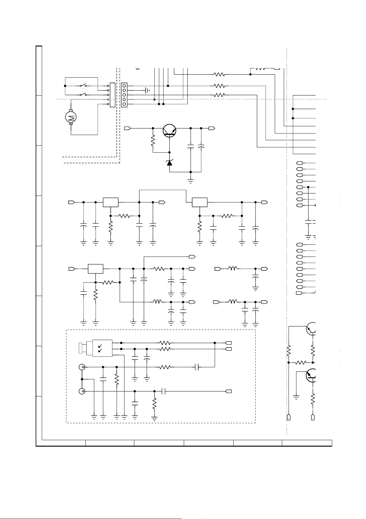
HT-CN150DVW
TRACK
5
GND
C
2
TRACK
A
B
SW803
SW804
M44
CN3
TRAY-SW1
TRAY-SW2
-
2
MICL
1
MICR
RB803
1
2
3
4
5
CN803
VCC
TP36
TP35
TP34
TP33
1
2
3
4
5
CLOSE SW
OPEN SW
DCLOAD-
DCLOAD+
Q201
KST2222(OPEN)
CLOSE
R815 1K
R816
R817
R818
VCC33V
CLOSE(189PIN)
1K
OPEN(191PIN)
0
CLOSEW(187PIN)
0
OPENSW(190PIN)
R270
4.7K
RF33V
3.3V
C834
R812
LM358
IC805-A
R811
100u/16
1
4K7
4
B-
0
1M
OPEN/CLOSE
MOTOR
C
IC208
5V
VCC
VCC
100u/16
C271
5V
C278 104
D
E
3
B1117N-33
0V
104
R253 0
C272
IC210
B1117N
0V
R257 0
2
1
R258
3
F
JK804
VIN
VCC
GND
G
JK805
100P
C840
1
2K2
3.3V
R254
R840 100
2
C279
1UF
3.3V
OPEN
C273
104
C838
104(OPEN)
R252 150(OPEN)
C274 100u/16
C280
100u/16(OPEN)
C841 100P
R259
220u/16
L203
C839
C842
R842 75
VCC33
1UH
R836
R837
R838
ZD201
4V6(OPEN)
2.2
C281 100u/16
C283 100u/16
100(0)
103
100(10)
0
C269
104
3.25V
VD33D
470P C282
3
0.8V
PLL33V
C284 104
C837
IC209
B1117N-18
1
R255 100(39)
RF33V
104(0)
C270
100u/16
2
+M5V
VCC
R256
2V
104
C275
150(330)
L204
L205
C276
104
1UH
1UH
C835
104
SPDIF-OUT
VCC
SPDIF-IN
VCC20
C277
100u/16
RF50V
C285
100u/16
C287
22Ou/16
TUN_B+/SW
MUTE
FERQ_HOP
TUN-CLK
TUN-CE
M62446-CLK
M62446-DATA
M62446-CE
4052-A
4052-B
SCART1
SCART2
WM8772-CLK
WM8772-CE
VFD-CE
VFD-CLK
MVCC
+5V
2SA733
75
R856
R857
Q808
2K2
30P
C261
L187
1K
R859
30P
30P
C263
C262
1UH
1K
R858
Q809
2SC2812N
R249
R250
R251
30P
C264
2K2
R860
RN211
C2
C
1
2K2
R861
H
1
23456
VCC
SCART1
SERVO CIRCUIT DIAGRAM (5/8)
28
Page 29
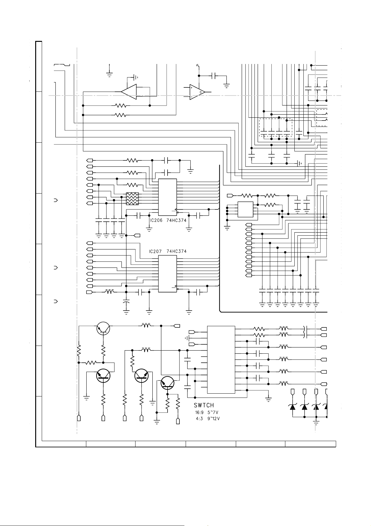
HT-CN150DVW
2
)
N
V
(189PIN)
91PIN)
A
(187PIN)
W(190PIN)
B
C
D
E
F
OUT
G
-IN
H
R270
4.7K
VCC20
C277
100u/16
RF50V
C285
100u/16
C287
22Ou/16
RF33V
TUN_B+/SW
FERQ_HOP
TUN-CLK
M62446-CLK
M62446-DATA
M62446-CE
WM8772-CLK
WM8772-CE
VFD-CLK
MUTE
TUN-CE
4052-A
4052-B
SCART1
SCART2
VFD-CE
+5V
MVCC
VCC
2SA733
75
R856
R857
Q808
2K2
3.3V
30P
C261
L187
1K
R859
SCART1
C834
LM358
IC805-A
R812
R811
30P
30P
C263
C262
1UH
1K
R858
Q809
2SC2812N
100u/16
4
1
0
4K7
R249
R250
R251
RN211 33 x4
30P
C264
2K2
R860
B-
1M
C265
C268
C288
10u/16V
2K2
R861
3.3V
3
2
33
33
33
104
VCC
104
L815
L816
Q810
2SC2812N
1K
R862
1uH
1uH
3.3V
2
5
6
9
12
15
16
19
20
10
12
15
16
19
20
10
C259
C260
30P
Q0
Q1
Q2
Q3
Q4
Q5
Q6
Q7
VCC
CLK
GND
2
Q0
5
Q1
6
Q2
9
Q3
Q4
Q5
Q6
Q7
VCC
CLK
GND
Q811
2SC2812N
R867
10K
30P
33K
R208
104
C223
C231
1UF
100P
100P
C245
C243
10u/16V
10u/16V
AIL
7V5(OPEN)
ZD814
R209
R210
47P
C224
100P
C237
100P
C244
7V5(OPEN)
ZD813
MVCC
5V
L830 1UH
5
B+
6
3
D0
4
D1
7
D2
8
D3
13
D4
14
D5
17
D6
18
D7
11
1
0E
C266 30P
3
D0
4
D1
7
D2
8
D3
13
D4
14
D5
17
D6
18
D7
11
1
OE
C267
BLNK
AIR
AIL
C860 15P
15P
R861
R866
1K
EN1
8
LM358
IC805-B
30P
C873
7
2
4
6
8
10
12
14
16
18
20
104
LD0
LD1
LD2
LD3
LD4
LD5
LD6
LD7
LCS1#
LD0
LD1
LD2
LD3
LD4
LD5
LD6
LD7
LCS2#
JK803
AIR
AGND
AIL
SWTCH
CLKOUT
DATA
DATAGND
BLNK
BLNKGND
VIN
VCC
VFD-DATA
WM8772-DATA
TUN-DATA
DAVN-RDS
AOR
AOL
BGND
GGND
RGND
VGND
VOUT
SHIELD
R226
IC205
1
SO
2
S1
3
S2
4
GND
SDA_RDS
SCL_RDS
TUN-ST
EN1
EN2
E-D(SW)
P-SCAN
1
3
5
7
B
9
11
G
13
15
R
17
19
21
M24CO2
IR
R864
VCC
SCL
SDA
C865
33
WC
C864
C866
C867
33P
C233
R863
152P
C230
152P
C229
473
C228
473
C227
33P
33P
C235
C234
R227
1K(5.6K)
5V
1K(5.6K)
R228
8
7
6
4.4V
5
4.4V
100P
100P
C239
C238
1K
1K
15P
L818
15P
L819
15P
L820
15P
L821
L822
100P
C240
L817
1uH
100P
C241
1uH
1uH
1uH
1uH
1uH
100P
C236
100P
C242
C862
C863
AIR
7V5(OPEN)
ZD815
R213
R215
B
104
C225
C232
AOR
AOL
B
G
R
VOUT
7V5(OPEN)
ZD812
C222
R221
R223
R224
RN201
RN202
RN203
RN204
G
OPE
C220
1K2
R
0
15K(0
153
IC204
3
VC
7V5(OPEN)
ZD811
R
1
23456
SERVO CIRCUIT DIAGRAM (6/8)
29
Page 30
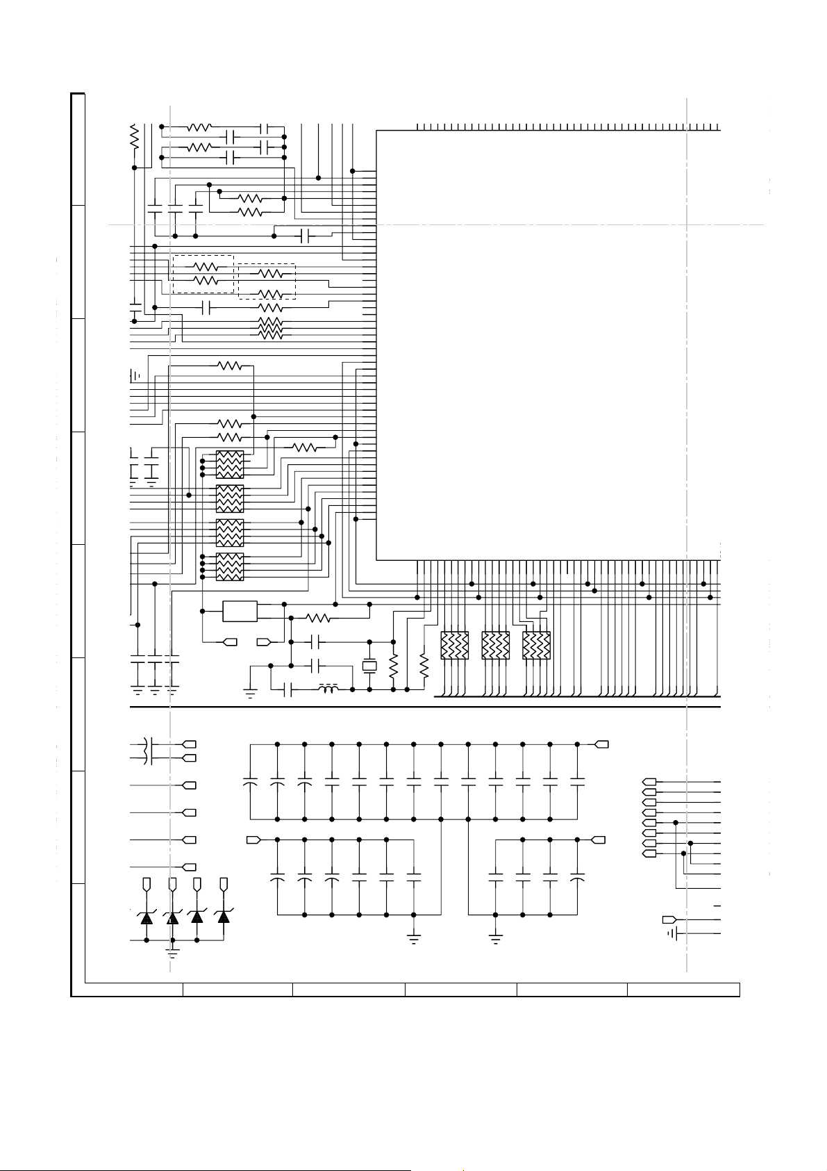
HT-CN150DVW
B
W
CC
L207
W
S
T
MCTSTSTST
227
228
4.4V
4.4V
33K
R209
A
R208
104
C223
R210
47P
C224
B
152P
C230
152P
C229
473
C228
473
33P
C
C234
1K(5.6K)
1K(5.6K)
D
33P
C235
100P
C236
C231
1UF
100P
C237
R213
R215
C232
OPEN
C220
1K2
C222
104
R211
C225
0
15K(0)
153
R221
R223 33
R224
RN201
RN202
C219
OPEN
C221
473
560P
R212 5K1
SVREF15
R214
R216
R217
R218
R219
R220
33
33
4K7 x4
33 x4
OPEN
10K
C226
0
0
6K8
33
33
33
CLOSE(189PIN)
R225
156
155
154
153
152
151
150
149
148
147
146
145
144
143
142
141
140
139
138
137
136
135
134
133
132
131
130
129
128
127
126
125
124
123
122
121
120
119
118
117
116
115
114
113
112
111
110
109
108
107
106
105
VSS
VDD
XSFEI
XSTEI
AVDD3_AD
XSVREF[21]
XSVREF[09]
XSVREF[15]
XSCEI
XSRFRP
XSSBAD
AVSS_AD
XSTEXI
XSFLAG[1]
XSFLAG[2]
XSFLAG[3]
XSTESTAD
IC201 ESS6629FD
XSIPIN
XSRFIP
XSRFIN
XSIREF
XSDSSLV
157
AVSS-DS
158
AVSS-PL
159
XSPDOFTR1
160
XSFD0
161
XSFTR0PI
162
AVDD3-PL
163
XSPLLFTR1
164
XSPLLFTR2
165
XSERVF0
XSCSJ
XSDATA
XSCLK
SDEFCT
SLDC
SPDON
166
167
168
169
170
171
172
173
174
175
176
177
178
179
180
181
182
183
184
185
186
187
188
189
190
191
192
193
194
195
196
197
198
199
200
201
202
203
204
205
206
207
208
XSAWRC
AVSS_DA
XSRFRPCTR
XSTRAY
AVDD3_DA
XSSPINDLE
XSFOCUS
XSSLEGP
XSSLEGN
XSTRACK
XSTESTDA
XSFGIN
XSPHOI
XSCSJ
XSDATA
XSCLK
XSDFCT
XSLDC
XSSPDONG
VDD33
VSS33
XGPIO(9)
XGPIO(8)
XGPIO(7)
XGPIO(6)
XGPIO(5)
XGPIO(4)
EAUX03
EAUX02
EAUX01
EAUX00
VSS
VDD
AUX0
AUX1
AUX2/HSYNC
AUX3/VSYNC
AUX4
AUX5
AUX6
AUX7
RESET
VS33
104
33
AVDD3_DS
XSLG
XSIP1
XSIP2
XSFLAG[0]
VS33
XSWBL
XSWBLCLK
VD33
MCLK
TBCK3
SPDIFIN
SPDIF/SEL_PLL3
TSD3
TSD2
VS33
YUV5/YDAC
YUV0/UDAC
YUV2/CDAC
TWS/SEL_PLL2
TSD1/SEL_PLL1
TSD0/SEL_PLL0
VS33_DA
VD33_DA
YUV6/VDAC
YUV4/RSET
YUV1/VREF
YUV7/FDAC
YUV3/COMP
R
RBC
R
VS33_PL
RN203
100P
C239
33 x4
RN204
4K7 x4
IC204
LM809
2
E
100P
100P
100P
100P
100P
100P
C240
C241
C242
C243
C245
C244
3
VCC
VCC33
RES
GND
1
RESET#
C248
C246
C247
102
R230
L201
10K
27P
27P
10UH
XL201 27MHz
100K
R231
XIN
VDD33
XOUT
DMAO
DCLK
213546789
0
RN205 10 x4
R232
MA1
MA0
DMA1
DMA2
DMA3
VS33
VD33
DMA4
DMA5
DMA6
DMA7
DMA8
DMA9
DMA10
VS33
MA7
VD33
RN207 10 x4
MA9
MA8
MA11
MA10
10111213141516171819202122232425262728293031323334353637383940414243444546474849505152
RN206 10 x4
MA2
MA3
MA5
MA4
MA6
DMA11
DCAS
CAS#
CSO#
DCS0
DCS1
RAS0#
DRAS0
VSS
VDD
DBANK0/DRAS1
DBANK1/DRAS2
DCKE/DOE/TDMTS
DWE#
DOE#
RAS2#
RAS1#
DWE
DB0
DB0
DB1
DB1
DB2
DB2
VS33
VD33
DB3
DB3
DB4
DB4
DB5
DB5
DB6
DB6
DB7
DB7
DB15
DB15
DB14
DB14
VS33
VD33
DB13
DB13
DB12
DB12
DB11
DB11
DB10
DB10
DB9
DB9
DB8
DB8
DSCK
DSCK
VS33
F
1uH
L817
1K
L818
L819
L820
G
L821
L822
1uH
H
1uH
1uH
1uH
1uH
7V5(OPEN)
C862
C863
AIR
ZD815
10u/16V
10u/16V
AIL
7V5(OPEN)
ZD814
B
7V5(OPEN)
ZD813
AOR
AOL
B
G
R
VOUT
G
7V5(OPEN)
ZD812
VCC
R
7V5(OPEN)
ZD811
10u/16V
C2001
10u/16V
C2002
220u/16
C2015
10u/16V
C2003
220u/16
C2016
104
C2004
10u/16V
C2017
104
104
C2018 C2005
104
C2006
104
C2019
104
C2007
104
C2020
104
C2008
104
C2009
104
C2010
104
C2021
104
C2011
104
C2022
104
C2012
104
C2023
104
C2013
VCC20
C2024
10u/16V
VCC33
R-IN1
L-IN1
SR1
SUB1
SL1
C1
L1
R1
P-SCAN
R352
R353
R354
R355
R356
R357
R358
R359
R360
R363
10
10
10
10
6K8
10
10
10
39K
39K
SW801
1P2T
1
23456
SERVO CIRCUIT DIAGRAM (7/8)
30
Page 31

HT-CN150DVW
137
C2012
104
MA10
DMA11
20
C2023
104
7
7
1
0
9
TBCK
MCLK
TSD2
TSD1
TSD0
TWS
136
135
134
133
132
131
130
129
128
127
126
125
124
123
122
121
120
119
118
117
116
115
114
113
112
111
110
109
VS33_DA
VD33_DA
YUV5/YDAC
YUV2/CDAC
108
YUV4/RSET
YUV7/FDAC
YUV6/VDAC
VSS
XSFLAG[2]
XSFLAG[3]
A
XSIP1
XSFLAG[0]
XSFLAG[1]
XSIP2
XSLG
XSWBL
VS33
VD33
SPDIFIN
XSWBLCLK
VS33
TSD3
TSD2
MCLK
TBCK3
SPDIF/SEL_PLL3
YUV0/UDAC
TWS/SEL_PLL2
TSD1/SEL_PLL1
TSD0/SEL_PLL0
B
IC201 ESS6629FD
C
D
VSS
VDD
DBANK0/DRAS1
DBANK1/DRAS2
DCKE/DOE/TDMTS
DWE
DB0
DB1
DB2
VS33
VD33
DB3
DB4
DB5
DB6
DB7
DB15
DB14
VS33
VD33
DB13
DB12
DB11
DB10
DCAS
DCS0
DCS1
DRAS0
21222324252627282930313233343536373839404142434445464748495051
DB9
E
DB9
DB10
DB11
DB12
CAS#
CSO#
F
G
RAS0#
RAS1#
104
C2013
VCC20
C2024
10u/16V
DOE#
RAS2#
DWE#
VCC33
DB0
R-IN1
L-IN1
SR1
SUB1
DB1
SL1
DB2
DB4
DB3
DB5
C1
L1
R1
DB6
DB7
DB15
DB14
R352
R353
R354
R355
R356
R357
R358
R359
R360
R363
DB13
10
10
10
10
6K8
10
10
10
39K
39K
C255
R243 0
107
106
105
VS33_PL
YUV1/VREF
YUV3/COMP
VD33_PLL
RWS/TDMFS
RBCK/TDMCLK
RSD/TDMDR
DB8
DSCK
VS33
52
VCC33
L207
60ohm
DSCK
DB8
6CH-7
6CH-8
6CH-5
6CH-6
6CH-3
6CH-4
6CH-1
6CH-2
LD7
LD6
LD5
LD4
VD33
VS33
LD3
LD2
LD0
LOE
LWRLL
CLS3
VDD
VSS
LCS2
LCS1
LCS0
LA0
LA2
VD33
VS33
LA3
LA4
LA5
LA6
LA7
LA8
VDD
VSS
LA10
LA11
LA12
LA13
LA14
LA15
VD33
VS33
LA16
LA17
LA18
LA19
LA20
LA21
DQM
VD33
C2040
LD1
LA1
LA9
104
5P
104
103
102
101
100
99
98
97
96
95
94
93
92
91
90
89
88
87
86
85
84
83
82
81
80
79
78
77
76
75
74
73
72
71
70
69
68
67
66
65
64
63
62
61
60
59
58
57
56
55
54
53
TSD[0:3]
VCC20
WM8
WM87
WM8772
1UH
L202
LD7
LD6
LD5
D80
245
DQ0
D81
DQ1
DB2
LCS3#
LCS2#
LCS1#
DQM
DB3
7
DQ2
LD4
LD3
LD2
LD1
LDD
LOE#
DB4
81011
DQ4
DQ3
LA21
DB5
DQ5
LA20
DB6
DB7
13
DQ6
LA19
DB8
424445
DQ8
DQ7
WRLL#
DB9
DQ9
LA0
LA1
LA2
LA3
LA4
LA5
LA6
LA7
LA8
LA9
LA10
LA11
LA12
LA13
LA14
LA15
LA16
LA17
LA18
LA19
DB10
DQ10
DB11
47
DQ11
LA19
LA18
LA8
LA7
LA6
LA5
LA4
LA3
LA2
DB12
DB13
485051
DQ12
LA16
LA15
LA14
LA13
LA12
LA11
LA9
LA8
LA18
LA7
LA6
LA5
LA4
LA3
LA3
LA1
LA0
LA10
LA17
LA16
LA15
LA14
LA13
LA12
LA11
LA10
LA9
DB14
DQ13
DQ14
IC203 4MX16Y
A8A9A10
A11
A0A1A2
232425
MA1
MA0
MA2
26
MA3
A3
A4A5A6
29
303132
MA5
MA4
MA6
MA7
A7
333422
MA8
MA9
MA10
35
MA11
0
R233
CLK
38
DSCK
37
DOE#
RSD
DB15
53
DQ15
CKE
11427
VCC
33
R234
C367
R242 0
VCC
VCC
BA1
BA0CSRAS
21
20
RAS1#
RAS2#
3
19
CS0#
C366
OPENR240
94349
VCCQ
VCCQ
18
RAS0#
R248
VCCQ
33 x4
RN208
VCCQ
C365
1
A16
2
A15
3
A14
4
A13
5
A12
6
A11
7
A9
8
A8
9
WE#
10
RESET
11
VPP
12
RDY/BUSY
13
A18
14
A7
15
A6
16
A5
17
A4
18
A3
19
A2
20
A1
1
A15
2
A14
3
A13
4
A12
5
A11
6
A10
7
A9
8
A8
9
NC
10
NC
11
WE
12
RESET
13
VPP
14
DU/WP
15
NC
16
A18
17
A17
18
A7
19
A6
20
A5
21
A4
22
A3
23
A2
24
A1
124652
6
VSSQ
VSSQ
CASWEDQML
17
16
15
39
33
33
DQM
N18270555
DWE#R236
CAS#R235
C364
R241
OPEN
A17
GND
A19/A-1
A10
DQ7
DQ6
DQ5
DQ4
VCC
VCC
DQ3
DQ2
DQ1
DQ0
0E#
GND
CE#
0
A16
BYTE
GND
DQ1515/A1
DQ7
DQ14
DQ6
DQ13
DQ5
DQ12
DQ4
VCC
DQ11
DQ3
DQ10
DQ2
DQ9
DQ1
DQ8
DQ0
GND
IC2
41
54
28
VSS
VSS
VSSQ
VSSQ
DQMHNCNC
36
40
33
R237
NC
NC
A0
A0
VSS
C363
G
E
C362
40
39
38
37
36
35
34
33
32
31
30
29
28
27
26
25
24
23
22
21
48
47
46
45
44
43
42
41
40
39
38
37
36
35
34
33
32
31
30
29
28
27
26
25
C254
C253
C252
C251
C250
C249
VCC
LOE#
LCS3#
LD7
LD6
LD5
LD4
LD3
LD2
LD1
LD0
C36
C36
LA17
LA0
LA1
104
104
104
104
104
104
LA20
LA19
L0E#
LCS3#
VCC33
LD7
LD6
LD5
LD4
LD3
LD2
LD1
LD0
C35
RWS
RBCK
RSD
SDM#[2:53]
6CH-[1:8]
H
P-SCAN
1
SW801
1P2T
23456
SERVO CIRCUIT DIAGRAM (8/8)
31
Page 32

HT-CN150DVW
T
9G
DISPLAY/STANDBY SCHEMATIC DIAGRAM
A
104
100u/10
C217A
4K7
C216A
B
10K
R245A
100
R246A
100
R247A
C
100
R248A
C218A
15P
R249A
R250A
R251A
R252A
C219A
R240A
15P
C220A
56K
R241A
1
S1
2
S2
3
S3
4
S4
5
DOUT
6
DIN
7
NC
8
CLK
9
15P
10K
10K
10K
10K
STB
10
K1
11
K2
12
K3
13
K4
515250
4948474645
OSC
GND
LED1
LED3
LED2
LED4
IC202A
TP6311
CDD
SG2/KS2
SG4/KS4
SG3/KS3
SG5/KS5
SG1/KS1
14
16
15
18
17
LED5
SG6/KS6
19
20
44
GR1
VDD
SG7/KS7
SG8/KS8
21
22
43
42
GR2
GR3
GR4
SG20/GR9
SG19/GR10
SG18/GR11
SG17/GR12
SG16/GR13
SG15/GR14
SG9/KS9
SG11 /K S11
SG10/KS10
23
24
41
40
GR5
GR6
GR7
GR8
VEE
VDD
GR15
GR16
SG12/KS12
25
26
LCR
LS S RS
DP201
AC2
F1
C221A 102
C223A
39
38
37
36
35
34
33
32
31
30
29
28
27
100u/35
P-SCAN
DIGITAL
AUDIO
PROLOGICII
SCAD
STEREOdts
NC
NC
F1
F1
1
2
56789
4
3
MP3VCD
1G2G3G4G5G6G7G
101112
8G
13
TI
DVD
D202
PREV
TA204
1N4148
1N4148
VOL-DN
TA209
VOL-UP
TA210
PROG
TA201
OPEN/CLOSE
TA206
2SA733(M6)Q201A
STOP
TA20 7
C
E
R232A
B
100K
22K
R231A
D
D203 1N4148
D201
2K2
2K2
E
2K2
R237A
R238A
R239A
10K
R242A
10K
R244A
10K
R243A
SOURCE
TA203
PL/PUTA205
TA202 NEXT
F
10K
10K
C205A
15P
100K
R215A
R213A
G
R216A 100K
10K
R214A
XL201A
15P
C201A
4MHz
15P
C202A
C204A
104
R212A
10K
Open
10K
R210A
R209A
R211A
104
C206A
100u/10
C207A
18
17
16
15
14
13
12
11
10
IC201A
OFF
F3
F2
F1
OSC2
OSC1
VDD
RES
HT48R05A
2K2
R217A
PROG
OP/CL
STOP
P-MUTE
PCON
POWER
VSS
5V1
ZD201A
IR
10K
10K
10K
10K
10K
10K
10K
10K
R207A
R206A
R208A
1
2
3
4
5
6
7
8
9
R205A
R204A
R203A
R202A
R201A
H
1
23456
DISPLAY/STANDBY CIRCUIT DIAGRAM (1/2)
32
Page 33

HT-CN150DVW
F1
TITLE
DVD
P-SCAN
R
DIGITAL
RS
NC
NC
4
3
102
STOP
TA20 7
AUDIO
PROLOGICII
SCAD
STEREOdts
VCD
1G2G3G4G5G6G7G8G9G
56789
C
B
E
2SA733(M6)Q201A
100K
R232A
MP3
1011121314151617181920212223242526272829303132333435363738
TRK PRESET CHP PROG SLEEP WAKEUP REPEAT1
10G
11G
12GNXNXNXNXNXNXNXP1P2P3P4P5P6P7P8P9
22K
R231A
C
Q202
E
2SA733(M6)
R234A
100K
C
B
Q203
E
2SA733(M6)
100K
R236A
22K
R233A
B
22K
R235A
100
R219A
100u/10
C208A
P10
R228A
P11
R224A
R222
P12
P13
104
C209A
P14
P15
39
1K5
470
1.2K
P16
C
Q204
2SC945
47K
R221A
A-B
KHz
MHz
NP
NPF2F2
404142
43
E
B
10K
R223A
C222A
F2
102
STBY
PLAY
AC2
T5V
PCON
P-MUT
IR
AC1
AC2
-24V
+5V
EN1(VOL-A)
EN2(VOL-B)
C212A
100P
5
4.7
0
4.3
4.5
4.5
-24
5
DGND
T5V
PCON
P-MUTE
GND
IR
AC2
AC1
-24V
+5V
V-DATA
V-CLK
V-CS
GND
V
5
V
0
V
4.7
4.3
V
0
V
0
V
0
V
0
V
16
161291
15
14
13
12
11
10
9
8
7
6
5
4
3
2
1
RB201
123
SN201
TO MAIN
PWB 5 PIN
CN202
(CNS201)TO MAIN
CN201
PWB 9 PIN
REMOTE-SENSOR1
CONNECTOR
CONNECTOR
CN202
CN201
470
RB202A RB202B
Q205
1
2
3
4
R218A
E
B
R253A 4K7
R254A
6
7
C
2SA733(M6)
10K
89101112
1
2
3
4
(STANDBY CIRCUIT DIAGRAM)
LD201
STANDBY
TA20 8
standby
DISPLAY/STANDBY CIRCUIT DIAGRAM (2/2)
33
Page 34

HT-CN150DVW
R
1
8
2
KARAOKE/MIC SCHEMATIC DIAGRAM
C805A
104
1
R805A 200K
C806A
10UF/25V
C826A
+
10UF/25V
C825A
7
+
4.7UF/50V
C830A
4.7UF/50V
22K
Q881A
-12V
O
C804A
R819A
56K
+
2SC945
IC803A
4
3
-B
100
Q8
C810A
+
4.7UF/50V
15
2
++
47UF/16V
47UF/16V
C837A
10UF/25V
R840A
100K
+
C838A
100UF/16V
R885A 10K
R808A
18K
R809A
10K10K15K
16
1
R839A
8.2K
C809A
102
IC801
+
4.7KR886
C808A
392
C819A
104
C824A
C824A
C807A
+
10UF/25V
R807A
10K
+5V
O
R837A
C834A
C836A
+
10UF/25V
R838A
100K
4
-B
-12V
IC802A
3
2
8.2K
100
C832A
104
7
IC802B
R806A
10K
+C822A
10UF/25V
R816A
100K
RC4558D
R833A
22K
R834A
1K
+12V
8
+B
O
RC4558D
8.2KR836A
C835A 100
10KR883A
C823A
104
5
6
5
6
R818A
OPEN
R832A
22K
2SC945
Q882A
C842A
+
10UF/25V
+12V
8
IC803B
RC4558D
+B
O
0R846A
OPEN C824A
C831A
47UF/16V
R831A
22K
R835A
1K R830A
+
R882A 1K
R845A
C815A
683
9
8
R848A
47
R848B
47
CN801A
8
7
6
5
4
3
2
1
47
10K(OPEN)
C811A
103
C812A
332
C817A
104
-12V
+12V
EN2
EN1
GND
MIC-L
MIC-R
OKDEC
C814A
10
7
C816A
104
683
R814A
10K
11
6
R817A
15K
R813A
12
5
10K
R812A
10K
C813A
102
13
4
C839A
+
100UF/16V
R811A R810A
14
3
C841A C818A
R841A
8.2K
A
B
C
D
E
+5V
C898A
104
ZD801
5.6V
Q807A
2N945
R849A
330
+
C866A
100UF/16V
+
C846A
100UF/16V
F
G
H
1
23456
KARAOKE/MIC SCHEMATIC DIAGRAM (1/2)
34
Page 35

-12V
A
4
-B
O
05A 200K
C804A
06A
F/25V
IC803A
100
RC4558D
3
2
R804A
1K
C803A
332
R803A
3.3K
C802A
+
1UF/50V
R802A
33K
R801A
33K
C801A
104
L801A
100UH
7
6
3
2
4
5
1
HT-CN150DVW
JK801A
R819A
56K
C826A
10UF/25V
C825A
4.7UF/50V
830A
+
.7UF/50V
R881A
10K
R820A
100
R824A
1M
R821A
47K
VR801A
50K
D802A
LL4148 1K
EN1
D801A
LL4148
R825A
15K
C828A
+
4.7UF/50V
Q803A
2SC945
R826A
33
D804A
LL4148
+C827A
100UF/16V
D803A
LL4148
R823A
220
R821A
R822A
47K
R827A
10K
+C829A
4.7UF/50V
ALC
Q801A
2SC945
R828A
10K
Q802A
2SC945
+5V
R829A
100
EN1
1A
1K
Q883A 2SC9452SC945
EN1-1
SCART-1
SCART-2
P-SCAN
7
10KR4001
R4002
R4003
R4004
10K
10K
10K
R4005 R4006 R4007 R4008
10K 10K 10K 10K
Q804A
2N945
8 9 10 11 12
R0001
11K
Q804B
2N945
R0002
27K
Q804C
2N945
R0003
47K
Q804D
2N945
R0004
47k(OPEN)
KARAOKE/MIC SCHEMATIC DIAGRAM (2/2)
35
Page 36

HT-CN150DVW
TUNER CIRCUIT DIAGRAM
A
100U
16V
C047
C048
104P
C010
R01
XTAL-10.7M-3
10 4P
C006
16V
C005
R008
C014
IF002
100U
220P
C028
220P
C027
152P
C033
2SC945
Q002
D003
1N4148
R032
100K
C045
5
4
6
1.2V
7
T003
1
1.2V
3
2
1.2V
0.7V
1.4V
1.2V
33
C019
32
1.4V
1V
1.4V
0.7V
1.4V
1V
1.4V
1.4V
0.8V
34
35
36
37
38
39
40
41
42
44
104P
C007
FM-IF12
Vstab(b)
FM-11
AM-IF2
FM-IF1-IN
Vstab(a)
FM ON/OFF
AM-MIXOUT
AM-IF-IN
RF-GND
FM-IN43
AGC
RIPPLE
1
2V
C008
16V
100U
AFC
AM-RF
2
0V
220
R006
FM12
470
R005
16V
10U
16V
100U
C004
10
470
22K
R030
R029
R016
R031
100K
100K
R033
C046
0V
0V
7.7V
7.9V
28
29
31
30
P1
P0
DATA
W/EN
TEA5762H
C-GND
AMOSC
RF-GND
FM OSC
34567
0.1V
T005
0V
AM-RF
AM-RF-A
CN002
CN2P-25
SCL
PSWO
C024
2.2UF
560P
C030
11
12
13
14
15
16
17
18
19
20
T002
B
C
D
C032
E
3
2
1
7
T001
6
5
4
F
8
OSC
7
IF OUT
220
R009
6
VCC
5
TUN-V
4
MT/GND
3
AGC
KST-F404
2
G
ANT-G
EF450-G1
ANT
ANT001
1
H
MAD
AFIN
VDDA
VSSA
MPX
Vref
BPFO
CMP
LVIN
4
3
XTAL-10.7M-3
2
IF001
0OHM
R040
10
R039
270
SDA
9
270 R038
DAVN
8
R034
470
IC002
VDDD
7
10
R024
VSSD
6
OSC
5
DSCO
4
TCON
3
MPDO
2
MPRO
1
5
6
7
1
3
2
1
120
R004
330
100
220
2K2 R002
47K
10K
C07D
5
L1
L-5X5
4
C069
33P
C002
D002
IN4148
IN4148
D001
R001
R003
R007
R036
R035
R037
68P
47P
8.664M
C-STL002
1K
47P
47K
C05
152P
0OHM
R046
Q001
2SA733
OOHM
62P
1
2
3
SCL
12
10
R028
0V
27
1
6
1
SDA
11
222P
C043
220P
C038
220P
C042
12P
C040
75K
XL1
262524
DIG-GND
BUS-CLOCK
VCC1
I-TUNE
8
7.8
1.6-8V
VD001
2
3
8
7
4
5
2
10
102P
R015
2
C049
C009
DAVN
C041
1.4V
9
56K
3
1uF
1
IN4148
9
R027
XTALOSC
VCD
1V
VR001
104P
D005
VC001
5V
150K
ST 0.2V
10
MO/ST
8
Q003
2SC945
100
R018
MONO 4.8V
23
VDD
VCC2
ST/MONO
AFC+
FM DEM
IF-GND
PILOT
RIGHT
LEFT
MUTE
AF OUT
11
0.7V
5
321
7
FS1
AFC-
CLOCK
CD3
16V
9.5V
MPX-IN
1.2V
C012
DATA
CN001CN12P-20CN12P-20
6
R023 330
11.1 V
22
2V
21
1.1V
20
1.1V
19
1V
18
17
1V
16
0.6V
15
0.6V
14
0.8V
13
0.15V
LPF
12
M474
4
100U
C044
R019
5
WRITE
3K3
T006
4
D004
ZD 11V
104P
R017
L-78K
GND
ROUT
LOUT
VCC 12V
1
2
3
470
470
R021
R020
C036
C039
M224
M224
153P
C023
153P
C022
CD1
22OU
16V
C1
104P
C034
104P
C029
C037
M474
IF003
10.7MHz
C072
10P
2.2UF
C025
2.2UF
C017
C021
M474
2K2
C026
M474
560P
120P
C071
C050
R025 120
120
223P
R026
C031
4.7K
VD002
470P
CD20
1K
R014
R01233K
R013
15P
C035
2
3
T004
4
47
R010
33P
C011
C018
2SA733
Q004
R011
22K
560P
C016
10P
C015
1
7
6
5
1
23456
TUNER CIRCUIT DIAGRAM
36
Page 37

POWER SCHEMATIC DIAGRAM
R
S
HT-CN150DVW
T5H 250V
A
CN1
250V 1KP
CY1
CY2
SO222
F1
CX1
250V 1KP
R5A
B
C
LF-18-LP3018D
FL2
275V/0.47u
R5B
1/2W 1M
1/2W 220
50V/0.1u
C101
1/4W 301
R101
D
835-1A-B-C
91
10K OHM
SCR1
5 OHM
RL1
HZ12C2 TA
NTC2
12K 1/4W
R102
2N5064
NCP 1200P60
IC1
NTC1
A
250V/4.7KP
CY8
250V/4.7KP
CY7
ZD101
24V
ZD7
91
GBU4J
CN02
1/2SL14
1/2W 680
R19
35V/220u
TVR10241
Z2
TVR10241
Z3
1/4W 1.5K
C4
0
R28
1N4148
1/2W 470K
R2
R15
500V/4.7KP
R1
1/2W 470K
C12
MPS2222A
Q6
R17
1/4W 15
R16
1/4W 15
47K/3W
R4
R3
P6KE300A 300V
EGP10D
1/4W 34.8
D2
R14
D7
1N4148
ZD1
C13
D8
E
50V/0.1u
C9
F
T901
B
G
1/2SL14
CN03
1/4W 47K
Q7
2N7000
H
HZ12C1 TA
D3
EGP10D
R8
ZD8
C6
50V/0.1u
1/4W 47K
1/4W 22K
R7
R12
1/4W 560
ZD4
HZ15-2 TA
1/2W 240
R26
R9
R10
1/4W 22K
C21
50V/0.1u
C8
25V/220u
Q8
2N7000
R11
1/4W 560
C7
25V/47u
-27V
ZD3
HZ7A1 TA
1/4W 10K
R18
1
23456
POWER SCHEMATIC DIAGRAM (1/2)
37
Page 38

HT-CN150DVW
ZD1
00A 300V
C13
0D
4.8
48
7u
1KV/0.01u
2W/24
R30
BYM26E
FB2
FQA8N80
R6A
2W/0.2
FB14
CY5
FB15
R13
1/4W 10K
IC2
SFH617A
C3
D1
FB1
Q1
FB3
FB16-17
R6B
250V/2.2KP
T1
500V/470P
C240
500V/470P
C310
C121
500V/2.2KP
500V/470P
C120
500V/470P
C243
R272
FB4 -27V
FB5
STTH2003CT
C246 500V/470P
C311 500V/220P
FB6
FB7
STTH2003T
R121
C123
500V/220P
FB8
FB9
STPR1020CT
FB10
FB11
STPS20H100CT
C683 500V/220P
1N4148D271
1N4148
D681
CR243
CR311
2W/10
CR121
CR681
1KR271
CR 1.05mH
L123
C242
50V/1Ku
C312
50V/1Ku
CD 14.5uH
C122
25V 680u
CB 0.53uH
C681
16V/2.2Ku
ZD5 20V
J18
L121
C124
16V/470u
L122
16V/1Ku
R301
1/4W 2.7K
1N4148D121
C682
C244
50V/100u
C314
50V/100u
R248
R243
2W 2K
R244
50V 0.1u
C317
ZD6
20V
R245
1/2W 1
R251
2W 2K
C245
50V/0.1u
+12V
C126
50v/0.1u
1/4W1.05K
-27V
+6.8V
R124
-27V
GND
+27V
C252
50V/0.1u
+12V
+6.8V
50v/0.1u
C684
D3
A
18
-27V
1/4W 10K
R29
0
Q5
MPS2222A
7
IC3
TL431ACZ-AP
C5
C315
50V 0.1u
C319
50V 0.01u
R312
1/4W 10K
1/4W 604
R316
C316
50V 0.1u
R314
1/4W 1K
8 9 10 11 12
POWER SCHEMATIC DIAGRAM (2/2)
+12VSB
ST
AC2
GND1
AC1
38
Page 39

IC’S Pin Voltage
HT-CN150DVW
PIN NO.
MODE
STOP
PLAY
PIN NO.
MODE
STOP
PLAY
IC802 AT5660, MOTOR DRIVER
1 2 3 4 5 6 7 8 9 101112 13 1819 2014 15 1716
1.5V 2.5V 2.5V 1.5V 2.5V 0V 0V 1.2V 1.2V 1.5V 6.1V 6.1V 2.5V 3.6V 5.0V 2.5V
1.5V 2.5V 2.5V 1.5V 2.5V 0V 0V 11V
21 22 23 24 25 26 27 28 29 30 31 32 33 38 39 4034 35 3736
12V 0V 1.5V 2.5V 2.5V 1.5V 1.5V 0V
11V 0V 1.3V 2.5V 2.5V 1.5V 1.5V 2.3V
5.2V 5.6V 5.6V 5.6V 2.5V 6.4V 5.0V2.5V 2.5V 4.7V2.5V
IC802
2.5V 2.5V 3.6V2.5V
2.5V
39
Page 40

HT-CN150DVW
t
WA VEFORMS
WF1 VIDEO OUT WF2 S-VIDEO OUT - Y Output
WF3 S-VIDEO OUT - C Outpu
Note :
WF1 ~ WF3 : Power On (Stop) Mode.
WF4 ~ WF7 : DVD Test Disc TDV-540A.
(Color Bar 75%)
WF4 COMPONENT VIDEO OUT - Y Output WF5 COMPONENT VIDEO OUT - Y Output
(Interlace mode) (P-Scan mode)
WF6 COMPONENT VIDEO OUT - Pb/Cb Output WF7 COMPONENT VIDEO OUT - Pb/Cb Output
(Interlace mode) (P-Scan mode)
40
Page 41

HT-CN150DVW
WF8 COMPONENT VIDEO OUT - Pr/Cr Output WF9 COMPONENT VIDEO OUT - Pr/Cr Output
(Interlace mode) (P-Scan mode)
WF10 Audio Left WF11 Audio Right
WF12 Rf Signal
Note :
WF8 ~ WF9 : DVD Test Disc TDV-540A.
(Color Bar 75%
)
WF10 ~ WF11 : DVD/CD Test Disc 1KHz, 0dB.
WF12 : Normal Disc.
41
Page 42

HT-CN150DVW
4
4
4
8
R484
MAIN PCB LAYOUT (TOP)
A
WIRING DIAGRAM
B
C
D
E
YUV PWB-A2
F
RB804
G
MAIN PWB-A1
R541
C5057
R543
R542
C5058
R544
C546
R525
C535
C531
R565
C536
C532
R526
C538
C537
C545
R501
C5053
R503
R522
C5055
R524
R521
C5056
R523
R502
C5054
R504
C501
R505
C505
R564
C506
C502
R506
R545
C575
C571
R566
C576
C572
R546
RB804
C516
C584
C585
C515
C578
C577
C510
C509
From Karaoke
PWB
RB801A
(CNS801)
CN901
C582
C587
C590
C588
C580
C586
R547
R527
R510
ZD501
C958
C959
R548
C548
R528
C960
C957
C518
C581
C
5
C541
C542
C
514
C511
C512
R511
C579
C589
C595
C583
43
C561
C560
C547
C539
C549
C562
C544
C521
C519
C517
C508
C522
C520
C513
C507
R563
Q501
R562
R561
R571
Q5992
R5983
GND9
R5891
R5967
ZD5992
O
1
IC503
IC502
O
1
1
O
IC501
JK806
Q5991
D5991
R5551
C5066
Q5050
C5065
C5063
R5552
R5982
C5991
C5064
C5061
C5062
C5042
ZD5041
R5050
*
C568
R
C5041
A
BC
D
E
C527
CF5042
CF5041
C951
R951
JK502
R952
C593
SRC
C955
C528
C952
C5087
SL
C5085
C5086
IC9550
C956
C567
Q404 Q405
R969
CN401
R466
R465
R496
C496
R468
R467
C598
SW
Q955
+6.V8
R988
R963
R658
R655
R656
R657
R670
R569
C983
R962
R968
+12V
CN908
C963
C5988
R965
R957
R961
C486
C485
ZD202
C478
C477
C490
ZD952
-27V
AC1
AC2
R006
C965
C5881
C301
R464
R452
R456
C483
R450
R956
R955
Q952
R954
R001
C471
C472
C973
C474
R451
C473
C475
C482
C479
R455
C481
R463
C491
R461
C492
C469
Q403
CN952
C453
R448
R449
C497
C431
R460
C463
R306
R301
CN202
CN903
R424
C436
R4021
C434
R4022
R421
R444
R465
R466
R442
R434
R436
C461
R475
R477
R479
R308
R305
R302
C302
R492
C480
C487
R470
Q409
C303
R303
C451
R486
IC404
IC406
JK401
C979
R429
R430
C458
C450
C452
R425
R426
R427
R428
C454
C467
R491
R432
C440
R485
R47
R307
R304
C
R
R
C971
C495
R960
C985
R260
C981
C961
R
C9882
IC953
4
62
GND8
R261
C488
C970
C476
R4007
R454
R453
C484
R458
R457
C494
C493
Q954
CN902
Q951
C4008
C986
IC407
IC409
IC408
R459
D960
C966
C5077
C5088
Q003
R050
C975
H
1
23456
MAIN PCB LAYOUT (TOP) (1/2)
42
Page 43

HT-CN150DVW
From Display
PWB
CN201
+12VS
MUTE
ST
CN202
CN903
C973
C471
C472
C480
C487
956
954
452
456
483
81
001
450
R470
955
C497
952
R424
R492
C453
C474
C436
R451
R4021
C434
C473
R4022
C475
R421
C482
C479
R455
C481
C431
R444
R465
R463
R466
C491
R461
C492
R460
C469
R442
R434
R436
C461
C463
Q409
R475
R448
C303
R477
R449
R303
R479
Q403
R308
R305
R302
R306
C302
R301
CN952
C451
R486
IC404
IC406
JK401
C979
R429
R430
C458
C450
C452
R425
R426
R427
R428
C454
C467
R491
R432
R485
R304
R478
R307
C433
R4024
R443
R484
C984
IC954
ZD401
R490
Q401
C304
C439C440
R487
R422
R4023
R423
C435
R420
C432
R440
R433
R435
C462
C410
C420
R481
C405
FB643
R0964
C430
R441
R431
Q473
R473
C457
IC405
C425
D318
R489
C415
C455
R483
R408
R471
C441
R409
R437
R438
FB644
R414
C423
R416
C417
C418
R482
R403
R402
-12V
R415
C403
C413
C429
R413
C419
C409
ON OFF
+12V
ECHO
CN801B
C977
ZD402
C456
C444
C438
R488
C422
IC403
R412
IC402
C412
R406
C408
IC401
C402
R445
R476
R472
R446
R474
C468
R447
C447
VANISH
Q408
R439
C446
C426
C449
C437
C445
M-L
Q402
R953
C464
R5006
D312
D313
D315
JK805
C428
R417
C404
M-R
C448
C427
R418
C421
C424
R498
R410
C414
R249
C259
C407
R404
R0001
R0003
C443
C442
R419
C416
R411
R407
C411
C406
R405
R321
Q804D
Q804C
Q804A
R401
C401
IR
R322
R0002
C265
R495
R496
R494
FB509
D314
D311
D301
R0004
R497
R493
R842
C841
R838
AC1
C263
D310
AC2
Q301
C5008
R848
C842
Q804B
C262
-24V
RN211
R311
R309
R310
R312
+5V
D316
D306
D305
D304
D303
R5009
R837
C837
FB642
FB640
R4145
R4141
R4148
R4144
R4147
R4143
R4142
R4146
R250
V-D ATA
V-CL K
CN201
Q5003
FB639
FB641
C264
C261
R251
R319
V-CE
D317
D308
D307
D309
D302
C313
C839
C266
ZD302
(CNS001)
T-L
FB506
FB501
FB505
RA301
C242
C243
C288
C2020
R266
R277
R228
IC204
C274
R237R233
C2017
C268
IC206
C260
C314
GND7
C838
JK804
From Tuner
PWB
CN001
(CNS001)
T-R
CN151
FB503
FB502
C2014
IC209
C237
C236
R256
R230
RN203
RN204
IC203
R6881
IC207
R363
R360
C316
IC301
C315
R315
R316
C312
JK802
+3V3
C2002
ZD301
R320
C311
RN202
R235
C2003
IC205
+3V3
R255
R355
C277
RN208
C8881
R353
R352
R234
R236
C115
C275
R225
XL201
RN205
RN206
RN207
IC2
R354
R356
C2001
RN201
C2040
CN951
D803
C240
R357
R359
R358
C926
R819
+3V3
From Pick-Up
PWB
FFC1
R826
R825
R812
R827
R811
C287
C827
C205
R245
IC351
ZD810
C216
C826
C226
C834
C825
R210
R209
C835
R807
C829
ZD201
ZD809
C830
CN801
C816
C831
C210
R206
C206
C207
C283
C822
C823
C209
C212
C211
C365
C359
ZD808
RF09
IC801
R203
R205
C819
C820
C204
C203
C269
Q201
RA351
C366
C364
ZD807
C854
RB804
C803
C201
C231
C846
R853
C807
C281
RN210
C270
C2015
C855
Q805
C812
C869
R804
C814
R244
C256
C255
R243
R252
R246
IC803
R888
C844
C289
R847
CN803
C833
R828
R821
IC802
R823
R223
R809
R830
R829
R815
R820
R810
R224
C2024
+2V
IC201
IC202
O
SUB
SR
C
C352
C354
C320
C357
C321
C358
C903
C904
R911
R912
L825
J-GND1
R806
C221
C220
C351
C922
C901
C921
C222
C219
R211
CN812
CN813
R831
R832
C967
IC805
R813
R814
R824
C235
R816
R822
R218
C233
C234
R214
R213
R220
R217
R215
R219
C367
R351
R241
C5999
C362
C859
C848
C850
R855
R854
R865
C353
C925
SL
C355
R
C356
L
LIN
R914
RIN
R916
R917
C902
R913
R4011
C4001
R4012
C4002
(CNS804)
Q806
C813
C815
C116
IC210
C291
R247
R849
R852
C856
CN804
C811
R259
C258
C5040
R805
R846
C868
RN209
RA352
R840
C840
C2031
C280
C2016
R851
C292
C271
R845
ZD806
ZD805
J-GND2
C832
C805
C806
C809
C801
ZD804
C808
C257
1
C285
D802
C804
D801
C817
R208
R202
R201
C208
R204
C202
R257
C278
C808
R850
ZD803
C2019
ZD801
ZD802
From YUV
PWB
(PWBA-2)
7
8 9 10 11 12
MAIN PCB LAYOUT (TOP) (2/2)
43
Page 44

HT-CN150DVW
C
MAIN PCB LAYOUT (BOTTOM)
A
B
C573 C574
C
C533 C534
D
C591
C592
C597
C596
C7893
C565
C563
C564
C566
C7892
R531
R532
R549
R550
R554
R553
R529
R530
C594
C599
R551
R555
R534
C569
R533
R5052
C5050
R5051
C5047
R5044
R5045
R5046
R5047
R5048
Q5042
C5051
Q5041
R5049
R5062
C5048
C5060
C5049
C5046
R5053
IC505
R5042
IC504
C5043
R5041
C5059
C5044
C5112
C5045
R5043
C5052
R967
C974
D951 C969
C7889
R4002
C976
R001B
R001A
C7888
C5113
C962
C964
E
C980
R4001
C4007
R4006
C4009
C4011
C5884
C5071
C5075
R4010
R4005
C5898
R4004
C4010
R4009
R4003
R4008
C12P1
C5879
C5876
R520
C5092
D501
R535
C5072
C5096
D502
R556
R970
C5091
C7891
C7890
E
C503
C504
C525
C523
C524
C526
R515
R516
R513
R514
F
C529R
C530
C570
R517 R518
D503
R536
C5095
D504
R519
C5094
D505
C5093
R552
D506
G
H
1
23456
MAIN PCB LAYOUT (BOTTOM) (1/2)
44
Page 45

R967
C980
EC21
R966
C001A
R001H
EC22
C7887
R001C
EC23
C978
R001F
EN2C1
EN2L1
R001G
R001D
EN1C1
C001B
R001E
EN1C2
EN2L2
R5003
D5551
Q5001
R5004
R5007
R5008
EN1L2
EN2C8
EN2L3
EN1C9
FC508
R0029
D5002
D5001
C5012
FB5003
C5882
FC506
C273
C251
FC507
FB508
C7882
FC501
FC502
FC503
C2013
C250
FC504
FC505
IC208
C7885
C238
C252
C253
C254
C241
C245
FB504
C247
R231
C7886
R232
C7883
C7884
R288
R289
C7881
C249
C2023
C2006
C2007
C246
R873
C248
R871
C2010
C871
C2004
C2005
C870
C244
C2022
C2008
C872
C7894
C239
R221
R833
C230
R216
C2027
C2021
C2012
C968
C2009
C232
C227
R271
C229
C276
C873
C217
C284
C270
C228
C218
C215
C290
HT-CN150DVW
RF08
C828 C818
C821
C810
C824
C802
R212
C224
C2011
C223
C225
C214
R207
C213
C2029
C2025
C282
C5839
C279
C272
C12P1
C267
R248
R242
R293
R240
C12P
C905
C906
IC941
R915
Q931
C5083
C286
C858
R836
R5060
C5074
7
8 9 10 11 12
C857
R870
C361
C852 C853
C360
C2026
C2018
C363
C851
C849
C363B
C363A
C847
C5838
C845
C5873
MAIN PCB LAYOUT (BOTTOM) (2/2)
45
Page 46

HT-CN150DVW
CONTROL PCB LAYOUT (TOP)
RB845B
3 2 1
4x4mm
A
TO CN845A
R228E
ABC D
C207A
4x6mm
C208A
SN201
B
TA203
TA210
TA202
TA204
TA211
TA201
TA209
C217A
VR801A
DISPLAY PWB-B1
(CNS855)
RB855B
From MIC
PWB
RB845B
From Display
PWB
(CNS845)
J3
C822A
C818A
C841A
CN845A
KARAOKE PWB-B3
C807A
C810A
C846A
E C B
8
Q807A
From MAIN
PWB
CN801B
(CNS801)
C825A
C866A
CN855A
C842A
C839A
RB801A
C826A
C829A
C837A
C802A
C806A
C831A
C836A
1
TO CN801A
C830A
C827A
C828A
C838A
XL201A
C
DP201
D
E
F
RB202B
From Standby
PWB
(CNS202)
RB202A
C223A
TA206
G
RB201
H
4x6mm
LD201
U-CS
U-CLK
TA208
+5U
U-DATA
STANDBY PWB-B2
1
23456
-24U
TA207
IR
AC2
AC1
P-MUTE
PCON
T5U
J3
1
RB202B
(CN201)
CN202
CN201
To MAIN PWB
3 2 1
RB855B
J1
TO CN855A
6
2
3
9
J2
5
JK301
4
1
78
C1
4x4mm
MIC PWB-B4
CONTROL PCB LAYOUT (TOP)
46
Page 47

CONTROL PCB LAYOUT (BOTTOM)
GND
EMC2
R228D
C202A
C204A
C201A
R228C
R228B
Q204A
Q201A
R240A
C205A
R233A
R234A
R224A
R221A
C212A
321
EMC1
R223A
R214A
R216A
C203A
IC201A
Q202A
Q203A
R235A
R236A
C206A
R217A
R237A
R243A
R238A
R244A
ZD201A
R239A
R242A
R228A
R213A
R215A
R212A
R211A
R210A
R209A
R218A
4x4mm
A
R222A
D9009
C209A
D9008
B
C
R219A
R208A
R207A
R206A
R205A
R204A
C221A
R203A
R202A
R201A
R231A
R232A
HT-CN150DVW
4x6mm
R832A
R810A
R811A
5
4
7
8
C823A
IC803A
C805A
C816A
R833A
R812A
R803A
R823A
R804A
C817A
R813A
C803A
C804A
R857A
R814A
R841A
R805A
R831A
D804A
C812A
L801A
R819A
R830A
IC802A
R829A
1
Q882A
R842A
R838A
R899A
C801A
R801A
R820A
R821A
R822A
Q884A
R802A
Q883A
R835A
C881A
Q881A
D803A
R836A
D802A
R886A
C835A
D801A
R825A
R826A
R824A
R828A
R827A
4x4mm
D9001
R252A
R251A
R250A
R249A
R246A
C216A
R255A
D9011
R256A
C218A
C219A
C220A
C9005
R245A
R241A
D9007
D9010
C9114
1
C9002
C9007
C222A
C9004
D9003
R218B
C9008
C9009
R253A
D9004
D9002
IC202A
Q205A
C9006
R254A
D9006
D9005
R248A
D203
D202
D201
R247A
D
E
F
G
GND
GND
H
C9010
4x6mm
C9003
C819A
R808A
C9012
R876A
R809A
C808A
C809A
R845A
C898A
J3
R807A
R848B
C9013
J1
R882A
3
FB302
C9014
J2
Q886A
R885A
R883A
IC801A
R849A
2
R881A
Q885A
Q880A
R848A
1
R816A
R817A
ZD801A
RB855B
R855A
6
2
3
9
R818A
C813A
C834A
R858A
C833A
R834A
R837A
R846A
R806A
C815A
C824A
R856A
C814A
C811A
R840A
1
23456
CONTROL PCB LAYOUT (BOTTOM)
47
Page 48

HT-CN150DVW
TUNER PWB LAYOUT (TOP)
TO MAIN
PWB
T004
C036
VR001
C017
CN151
C01
Q003
D004
C025
A
B
C039
C
C043
R031
R032
C03
C042
(CNS001)
C038
C044
C05
XL2
XL1
Q002
CN001
CN001
C033
C027
C014
R035
R01
C028
R024
C010
C047
C02
C048
C024
C030
T003
D003
I
C005
C001
C046
CO19
C045
R005
IF002
T002
IF001
T001
C009
C008
IF003
C037
C029
C004
D
T006
VD001
VD002
E
T005
VC001
EF450-G1
F
G
CN002
D006
H
1
23456
D001
D002
ANT001
L004
TUNER PWB LAYOUT (TOP)
48
Page 49

TUNER PWB LAYOUT (BOTTOM)
C069
HT-CN150DVW
A
C003
C070
C002
R040
R036
R037
B
Q004
C031
R026
R007
R046
C032
T002
R025
R014
R013
R012
C050
C
D
R009
R004
T001
E
C018
C020
C006
Q001
EF450-G1
R008
C021
R017
C007
C026 R002
C049
R003
R001
R006
VD001
C071
C012
D005
R02
T006
IC001
C072
C040
R018
R029
C011
R010
R033
R019
R023
R030
T003
R027
F
G
C04
C013
IC002
Q002
R039
R038
R034
C041
R016
XL2
R028
VD002
C034
C1
Q003
R020
C035
C022
R011
VR001
C023
R015
R021
C016
C015
T004
H
1
23456
TUNER PWB LAYOUT (BOTTOM)
49
Page 50

HT-CN150DVW
POWER PWB LAYOUT (TOP)
A
B
C
D
E
F
G
H
1
23456
POWER PWB LAYOUT (TOP)
50
Page 51

POWER PWB LAYOUT (BOTTOM)
A
B
C
HT-CN150DVW
1
2
3
7
6
5
4
D
5
E
8
9
2950154401
141713
F
G
10
H
1
23456
POWER PWB LAYOUT (BOTTOM)
51
Page 52

HT-CN150DVW
POWER PWB LAYOUT (COMPONENTS)
WARNING: UTILISER UN FUSIBLE DE RECHANE DE MEME TYPE
ZD7
NTC2
T901
R102
C102
CX2
B
J12
R101
J13
SCR1
CN03
ATTENTION:
THEREISAHI-POTAREA
FOR CONTINUED
PROTECTION AGAINST
RISK FIRE REPLACE
WITH SAME TYPE
CY8
WARNING:
J11
ZD8
D3
A
CR1
CR2
R5A
R5B
CX1
A
J14
R2
D7
CY2
Z1
CY1
B
T5H 250V
F1
CN1
C1
R1
Z2
C2
C
C3
R3
R30
R4
C12
ZD1
Q6
R17 R16
NTC1
Z3
R14
GT1
R13
CN02
R6B
G
FL2RL1
R6A
J17
C4
R28
Q1
D
HS1
D1
CY7
T1
E
D2
R15
C10
1
IC1
D8
R19
C21
ZD4
ZD101
J26
C7
J16
C9
J15
R26
C8
R9
R29
Q5
C5
Q8
R10
C6
R272
R18
C316
R124
R245
C319
R314
R11
ZD3
D121
C317
+6.8V
J28
J22
R243
Q7
C126
R316
R12
R8R7
GND
+12V
GND1
AC1 AC2 ST+12VSB
-27V
IC2
CY5
CY3
C243C120
F
G
H
1
TPS260300-0005 110/230V
C121
HS2
R121
C13
0
L121
C681
C123
J18
R244
CR121
C683
J20
C124
C122
J25
L122
CR681
R248
C130
J23
C134
C684
C240
CR311
R311
+27V
J24
C252
C862
GND
23456
R301
D271
D681
C246
ZD5
C312
L123
J21
C245
ZD6
R271
IC3
CR243
-27V
1
C315
R312
C242
C244
POWER PWB LAYOUT (COMPONENTS)
52
Page 53

SYSTEM CONTROL TIMING CHARTS
Tray Close ~ Play / Play ~ Tray Open
HT-CN150DVW
Tray IN
(CN803 pin 1/
IC201 pin 187)
Sled Drive
(IC802 Pin 12)
Disc Drive
(IC802 pin 17)
Focus Drive
(IC802 pin 14)
Tracking Drive
(IC802 pin 15)
3.3V
0V
1.65V
0V
1.65V
0V
1.65V
0V
1.65V
0V
Tray
Close
Disc
Rotation
Play Tray
Stop
Tray
Open
53
Page 54

HT-CN150DVW
IC PIN FUNCTION DESCRIPTIONS
IC401, DUAL WIDE BANDWIDTH OPERATIONAL AMPLIFIERS (RC4558)
Pin Configuration: Pin Description:
8
1
IC301,4 CHANNEL MULTIPLEXER (D4052)
Pin Configuration:
VDD
IN/OUT
2x
16
15 14 13 12 11 10 9
OUT/IN
1x 0x 3x A Bx
D4052BM
IN/OUT
Pin No.
1
2
3
4
5
6
7
8
Function
Output A
Input A
Input A
Vee
Input B
Input B
Output B
Vcc
Block Diagram:
INH
12 345 6 87
Y 2Y 3Y 4Y INH VEE VSSY
0
OUT/IN
IN/OUTIN/OUT
TOP VIEW
X CHANNELS IN/OUT
22110
3
11 15 14 12
TG
TG
VDD
16
10
A
9
B
5
LOGIC
LEVEL
CONVERSION
8
SS VEE
V
BINARY
TO
1 OF 4
DECODER
WITH
INHIBIT
7
0
Y CHANNELS IN/OUT
TG
13
3
COMMON X
OUT/IN
COMMON Y
OUT/IN
TG
TG
TG
TG
TG
4251
3
54
Page 55

IC805,DUAL OPERATIONAL AMPLIFIERS (LM358MX)
Pin Configuration: Block Diagram:
HT-CN150DVW
1OUT
1IN-
1IN+ 2IN-
2
3
4
8
7
6
5GND
Vcc1
2OUT
2IN+
OUTPUT A
NON-INVERTIN G
INPUT A
GND
Symbol (each amplifier)
IN+
IN-
+
-
OUT
IC501,DUAL D-TYPE FLIP-FLOP (CD4013BT/HEF4013BT)
1
2
A
-
3
4
++
8
+
V
7
OUTPUT BINVERTING INPUT A
B
6
INVERTING INPUT B
5
NON-INVERTING
INPUT B
!
Block Diagram:
V
DD
14 13 12 11 10 9 8
Q1 Q1
F/F
1
Q2
Q2
CLOCK 1 RESET 1 DATA 1 SET 1
CLOCK 2 RESET 2 DATA 2 SET 2
F/F
2
7654321
V
SS
55
Page 56

HT-CN150DVW
IC301, 4 CHANNEL MULTIPLEXER (D4052BM)
Pin Configuration:
Block Diagram:
VDD
IN/OUT
2x
16
15 14 13 12 11 10 9
OUT/IN
1x 0x 3x A Bx
IN/OUT
D4052BM
12 345 6 87
Y
2
0
Y
OUT/IN
3
Y
4
Y
IN/OUTIN/OUT
TOP VIEW
INH V
EE
V
SSY
X CHANNELS IN/OUT
3
22110
11 15 14 12
INH
TG
TG
VDD
16
10
A
9
B
5
LOGIC
LEVEL
CONVERSION
8
V
SS VEE
SINARY
TO
1 OF 4
DECODER
WITH
INHIBIT
7
0
Y CHANNELS IN/OUT
3
TG
13
3
COMMON X
OUT/IN
COMMON Y
OUT/IN
TG
TG
TG
TG
TG
4251
56
Page 57

IC504, CMOS Hex Inverter IC (74HCU040D)
Pin Configuration:
HT-CN150DVW
Schematic Diagram:
V
cc
AB Y6 Y5
14 13 12 11 10 9 8
1 234567
A5
Y2Y1 A2A1
A3
A4 Y4
Y3
Top View
V
cc
AY
57
Page 58

HT-CN150DVW
IC208, 1A Fixed & Adj Low Dropout Positive Voltage Regulators (RT9164-33CLR)
Pin Configuration:
Pin Description:
Block Diagram:
123
Pin Name
ADJ/GND
VOUT
VIN
Pin No.
1
2
3
Pin Function
Adjust or Ground
Output
Positive Power Input
Name
ADJ/GND
Vout
Vin
VIN
CURRENT
LIMITING
AMPLIFIER
THERMAL OVERLOAD
VOLTAGE
REGULATION
AMPLIFIER
LIMIT
SENSE
V
REF
S.O.A
VOUT
ADJ/GND
58
Page 59

IC801A, Echo Processor IC (PT2399)
Block Diagram:
HT-CN150DVW
LPF1 - IN16LPF1 - OUT15LPF2 - OUT
COMP
LPF 1
1/2 Vcc
AUTO
RESET
1
VCC
2
REF
14
MODIMI
44K Bits
RAM
LPF2 - IN13OP2-OUT12OP2-IN11OP2-IN10OP1-OUT
4.7K 4.7K
LPF2
3
AGND
4
DGND
9
DO0 DO1
5
CLK_0
MOD
CC0
8
CLOCK
VCO
6
VCO
CC1
7
DEM
Pin Configuration:
VCC
REF
AGND
DGND
CLK_O
VCO
CC1
CC0
1
2
3
4
5
6
7
16
15
14
13
12
11
10
8
9
LPF1-IN
LPF1-OUT
LPF2-OUT
LPF2-IN
OP2-OUT
OP2-IN
OP1-IN
OP1-OUT
59
Page 60

HT-CN150DVW
Echo Processor IC (PT2399)
Pin Description:
Pin Name I/O Description Pin No.
VCC - Analog Supply Voltage Input 1
REF - Analog Reference Voltage (=1/2VCC) 2
AGND - Anolog Ground 3
DGND - Digital Ground 4
CLK_0 O System Clock Output Pin 5
VCO I Frequency Adjustment Pin 6
CC1 - Current Contol 1 7
CC0 - Current Contol 0 8
OP1-OUT O
OP1-IN I
OP2-IN I
OP2-OUT O
LPF2-IN I Low Pass Filter 2 Input Pin 13
LPF2-OUT O Low Pass Filter 2 Output Pin 14
LPF1-OUT O Low Pass Filter 1 Output Pin 15
LPF1-IN I Low Pass Filter 1 Input Pin 16
OP Amplifier 1 Output This pin can be used as Modulated Integrator by connecting
Capacitor.
OP Amplifier 1 Intput This pin can be used as Demodulated Integrator by connecting
Capacitor.
OP Amplifier 2 Input This pin can be used as Demodulated Integrator by connecting
Capacitor.
OP Amplifier 2 Output This pin can be used as modulated Integrator by connecting
Capacitor.
9
10
11
12
60
Page 61

HT-CN150DVW
IC204, Micropower Supply Voltage Supervisor (CM3403)
Pin Description:
GND
1
3
RESET
2
3-pin SOT23
Pin Description:
PIN(S) NAME DESCRIPTION
1 GND Negative reference for all signals.
2 RESET
3VCCSupply input signal which is monitored by the sense comparator. This input is compared to the 2.93V
Active low reset output. When the sence threshold has been exceeded, the RESET signal will remain
active for an additional 140(min.) after which it is taken inactive. During a "brownout" condition, RESET
will immediately be taken active. Internal circuitry ensures RESET
ply voltage is as low as 0V.
(CM3403-29ST) or 4.63 (CM3403-46ST) reference to determine the state of the output.
V
CC
will remain active even when the sup-
Typical Application Circuit
V
IN
CM3403 Microprocessor
V
CC
RESET RESET
V
CC
GND GND
61
Page 62

IC802, 5-Channel Motor Driver for DVD/VCD (AT5660)
Pin Description:
HT-CN150DVW
28
2627 25 24 23 22
PGND
21 20 19 18 17 16 15
AT5660
32
1
4 5 6 7 8 9 10 11 12 13 14
Pin Description:
PIN NO. Pin name Function
1 IN1 CH1 (Focus coil) input
2 CAP1_1 CH1 error amplifier filter capacitor connection 1
3 CAP1_2 CH1 error amplifier filter capacitor connection 2
4 IN2 CH2 (Sled driver) input
5 FB1 CH1 (Focus coil) feedback pin
6 FWD CH5 forward input
7 REV CH5 reverse input
8 VCC1 Power Supply 1
9 OUT5- CH5 (Tray driver) output (-)
10 OUT5+ CH5 (Tray driver) output (+)
11 OUT2- CH2 (Sled driver) output (-)
12 OUT2+ CH2 (Sled driver) output (+)
13 OUT1- CH1 (Focus coil) output (-)
14 OUT1+ CH1 (Focus coil) output (+)
15 OUT4+ CH4 (Tracking oil) output (+)
16 OUT4- CH4 (Tracking oil) output (-)
17 OUT3+ CH3 (Loader) output (+)
18 OUT3- CH3 (Loader) output (-)
19 VCC2 Power supply 2
20 FB4 CH4 (Tracking oil) feedback pin
21 VCTL CH5 Speed control input
22 GND Ground
23 IN3 CH3 (Loader) input
24 CAP4_2 CH4 error amplifier filter capacitor connection 2
25 CAP4_1 CH4 error amplifier filter capacitor connection 1
26 IN4- CH4 (Tracking drver) input
27 VBIAS VREF input pin
28 MUTE_1_2_3_4 Mute control for CH1, CH2, CH3, CH4
Notes: The indicated polarities for the output pins are under the condition that all inputs are (+).
The power supplies for the driver output are PVcc1 for the loader, PVcc2 for focus and tracking drivers, and Vcc for pre-block and sled
driver, Therefore, make sure Vcc > PVcc1, 2.
PGND
62
Page 63

HT-CN150DVW
IC802, 5-Channel Motor Driver for DVD/VCD (AT5660)
Block Diagram:
IN1
CAP1_1
CAP_2
IN2
FB1
FWD
REV
PGND
VCC1
OUT5-
OUT5+
OUT2-
OUT2+
10
11
12
+
l
10K
1
7.5K
20K
+
l
TSD
2
3
4
5
6
10K
7
20K
7.5VK
10K
20K
+
l
7.5K
20K
20K
+
l
7.5K
STAND-
BY
10K
20K
28
27
26
25
24
23
22
MUTE
1_2_3_4
VBIAS
IN4-
CAP4_1
CAP4_2
IN3
GND
PGND
VCC1
Pre-DRV
8
9
TRAY
DRIVER
10K
25k
_
++
SLED
DRIVER
VCC1
VCC1
LOADING
10K
_
15K
DRIVER
10K
10K
VCC2
21
20
19
18
17
VCTL
FB4
VCC2
OUT3-
OUT3+
OUT1-
OUT1+
13
14
ACTUATOR
DRIVER
VCC2
ACTUATOR
DRIVER
16
15
OUT4-
OUT4+
63
Page 64

IC202A, VFD Driver (PT6311)
Pin Description:
Pin Name I/O Function Pin No.
SW1 to SW4 I General Purpose Input Pins 1 to 4
DOUT O
DIN I
NC - No Connection 7
CLK I
STB I
K1 to K4 I
VDD - Logic Power Supply 14, 33, 45
SG1/KS1 to SG12/KS12 O
SG20/GR9 to SG19/GR10
SG18/GR11 to SG13/GR16
VEE - Pull- Down Level 34
GR1 to GR8 O High- Voltage Grid Output Pins 44 to 37
LED1 to LED5 O LED Output Pin 50 to 46
GND - Ground Pin 51
OSC I
O High Voltage Segment / Grid Output Pins
HT-CN150DVW
Data Output Pin (N-Channel, Open-Drain) This Pin outputs serial data at the falling
edge of the shift clock (starting from the lower bit )
Data Input Pin
This Pin inputs serial data at the rising edge of the shift clock
(starting from the lower bit )
Clock Input pin
This Pin reads serial data at the rising edge and
outputs data at the falling edge.
Serial Interface Strobe Pin
The data input after the STB has fallen is
processed as a command.
When this pin is “HIGH”, CLK is ignored.
Key Data Input Pins
The data inputted to these pins are latched at
the end of the display cycle.
High- Voltage Segment Output Pins
Also acts as the Key Source
Oscillator Input Pin
A resistor is connected to this pin to determine
the oscillation frequency
5
6
8
9
10 to 13
15 to 26
36 to 35
32 to 27
52
64
Page 65

HT-CN150DVW
IC202A, VFD Driver (PT6311)
Block Diagram:
DIN
DOUT
CLK
STB
VDD
R
OSC
SW1
SW2
SW3
SW4
Serial
Data
Interface
OSC
General
Input
Register
Display Memory
(20 bits X 16 works)
Timing Generator
Key Matrix Memory
Control
Segment
Driver/
Grid
Driver/
Key Scan/
Output
SG1/KS1
SG2/KS2
SG3/KS3
SG4/KS4
SG5/KS5
SG6/KS6
SG7/KS7
SG8/KS8
SG9/KS9
SG10/KS10
SG11/KS11
SG12/KS12
SG13/GR16
SG14/GR15
SG15/GR14
SG16/GR13
SG17/GR12
SG18/GR11
SG19/GR10
SG20/GR9
LED1
LED2
LED3
LED4
LED5
LED
DRIVER
Dimming Circuit
K1 K2 K3 K4 VDD GND VEE
Grid
Driver
GR1
GR2
GR3
GR4
GR5
GR6
GR7
GR8
65
Page 66

IC 202A, VFD Driver (PT6311)
Pin Configuration:
OSC
GND
LED1
LED2
LED3
LED4
LED5
VDD
GR1
GR2
GR3
41 404243444546474849505152
GR4
HT-CN150DVW
GR5
SW1
SW2
SW3
SW4
DOUT
DIN
CLK
STB
NC
K1
K2
K3
K4
10
11
12
13
39
1
2
3
4
5
6
7
8
9
38
37
36
35
34
33
32
31
30
29
28
27
25 262423222120191817161514
GR6
GR7
GR8
SG20/GR9
SG19/GR10
VEE
VDD
SG18/GR11
SG17/GR12
SG16/GR13
SG15/GR14
SG14/GR15
SG13/GR16
VDD
SG1/KS1
SG2/KS2
SG3/KS3
SG4/KS4
SG5/KS5
SG6/KS6
66
SG7/KS7
SG8/KS8
SG9/KS9
SG10/KS10
SG11/KS11
SG12/KS12
Page 67

HT-CN150DVW
IC801, ESS DVD SERVO (ES6603S)
Pin Configuration:
IC801, ESS DVD SERVO (ES6603S)
SDEN
SDATA
SCLK
V33
48 3647 46 45 44 43 42 41 40 39 38 37 35 34 33
LCP
MNTRCEFE
LCN
TE
PI
V25
V125
TPH
DFT
LINK
RX
MEV
VNA
FNN
FNP
DIP
DIN
BYP
RFAC
VPA
AIP
AIN
ATON
RFAC
ATOP
RFSIN
RFDC
ATON
ATOP
RFSIN
RFDC
RX
MEV
VNA
FNN
FNP
DIP
DIN
BYP
VPA
AIP
AIN
49
50
51
52
53
54
55
56
57
58
59
60
61
62
63
64
SDEN
SDATA
SCLK
V33
LCP
48 3647 46 45 44 43 42 41 40 39 38 37 35 34 33
49
50
51
52
53
54
55
56
57
58
59
60
1 13
23456789101112
61
62
A2
B2
63
64
DVDRFP
DVDRFN
1 13
23456789101112
C2
MNTRCEFE
LCN
TE
ES6603S
ES6603S
D2
CP
CN
D
B
C
PI
V25
A
CD_D
V125
TPH
14 15 16
CD_B
CD_C
14 15 16
32
31
30
29
28
27
26
25
24
23
22
21
20
19
18
17
MEVO
MIN
MLPF
MB
MP
MEVO
MIRR
MIN
LDON
MLPF
VNB
MB
CDPD
MP
DVDPD
MIRR
CDLD
LDON
DVDLD
VNB
VC
CDPD
VPB
DVDPD
CD_E
CDLD
CD_F
DVDLD
VC
VPB
CD_E
CD_F
32
31
30
DFT
LINK
29
28
27
26
25
24
23
22
21
20
19
18
17
CD_A
FP
FN
FIGURE 1 ES6603 DEVICE PINOUT
A2
B2
C2
D2
CP
CN
67
B
D
C
A
_D
_C
_B
_A
Page 68

HT-CN150DVW
IC801, ESS DVD SERVO (ES6603S)
Pin Description:
Table 1 lists the pin descriptions for the ES6603.
The pound symbol (#) iindicates an active-low signal.
Table 1 ES6603 Pin Descriptions List
Name Pin Numbers I/O Definition
DVDRFP,
DVDRFN
A2,B2,C2,D2 3:6 I
CP,CN 7,8 - Differential phase tracking low-pass filter pins. Connect CP to CN via capacitors.
D,C,B,A 9:12 I Photo detector interface inputs from the main beam photo matrix.
D_D,CD_C,
CD_B,CD_A
CD_F,CD_E 17, 18 I
VPB 19 P Servo block power supply.
VC 20 O Reference voltage out (VPB/2).Output impedance is less than 50Ω.
DVDLD 21 O DVD APC output; controls laser power for DVD.
CDLD 22 O CD APC output; controls laser power for CD.
DVDPD 23 I DVD APC input.
CDPD 24 I CD APC input.
VNB 25 G Serve block ground.
LDON 26 I APC On/Off control. A high level activates LD output. (open is low)
MIRR 27 O Mirror detect output.
MP, MB 28, 29 I Mirror top and bottom hold pins. Connected to VPB pin 19 via capacitors.
MLPF 30 I Mirror low-pass filter pins. Connected to VPB pin 19 via a capacitor.
MIN 31 I RF input signal for mirror. AC coupled inputs for the mirror detection circuit from MEVO pin 32.
MEVO 32 O RFDC bottom envelope out. Pull-In or bottom clamped RF envelope signal ouptut for mirror detection.
LINK 33 I,O
DFT 34 O
TPH 35 I Pull-In top hold. Connected to VPB pin 19 via a capacitor.
V125 36 O 1.25V servo block reference voltage output.
V25 37 P 2.5V servo output reference power supply.
PI 38 O
TE 39 O Tracking error output reference to V125 pin 36.
FE 40 O Focusing error output reference to V125 pin 36.
CE 41 O Center error output reference to V125 pin 36.
MNTR 42 O Monitor out signal. Output is selectable by register settings.
LCN,LCP 43, 44 I Lens shift offset cancellation low-pass filter pins. Connect LCN to LCP via a capacitor.
V33 45 P 3.3V output buffers power supply.
SCLK 46 I Serial clock from ES66x8.
SDATA 47 I/O Serial data I/O
SDEN 48 I Serial data enable. Enabled by an active-high signal.
RX 49 I Reference resistor. Connected to ground via a 12.0kΩ, 1% resistor.
1,2 I Differential RF signal attenuator inputs.
AC coupled photo detector interface inputs for the differential phase detector (DPD) from the main
beam photo matrix.
13:16 I CD photo detector interface inputs from the main beam photo matrix
CD photo detector interface inputs from the CD side beam photo detector, used for CD tracking
detection.
Linking Signal In/Mirror Monitor Out. In the linking area, the mirror and
tracking error outputs are disabled when this pin goes high. When the monitor
output signal is selected by the Control H register, mirror-related signals can be observed.
Defect output. When the Pull-in signal level is below the detection level, or when the RF signal level is
below the detection level, the DFT output goes high. The defect output is selected by the serial port.
Pull-In signal out. The summing signal output of A, B, C, D or CD_A, CD_B, CD_C, or CD_D. Reference to V25/3.
68
Page 69

HT-CN150DVW
Name Pin Numbers I/O Definition
MEV 50 I RFDC bottom envelope. Connected to VPA pin 58 via a capacitor.
VNA
FNN, FNP 52, 53 O
DIP, DIN 54, 55 I
BYP 56 I
RFAC 57 O
VPA 58 P
AIP, AIN 59, 60 I Differential AGC amplifier inputs.
ATON, ATOP 61, 62 O Differential attenuator outputs.
RFSIN 63 I
RFDC 64 O
AGC Interface 59,60 I Differential AGC amplifiers inputs [AIP] AND [AIN].
Automatic Laser
Power Control
(APC) Interface
CD/DVD Photo
Detector Interface
Embedded Servo
DSP
Interface
Filtering and
Reference Voltage
Power and
Ground
51 G RF block and serial port ground.
Differential outputs of equalizer/filter.
Differential analog inputs to the RF single-end output buffer and full wave rectifier.
AGC amplifier gain bypass. Tied to VPA via a capacitor.
Single-ended RF output.
RF block and serial port power supply.
Single-ended RF signal attenuator input.
Single-ended RF summing output.
21 O APC laser power control for DVD [DVDLD].
22 O APC laser power control for CD [CDLD].
23 I APC photo diode in for DVD [DVDPD].
24 I APC photo diode in for CD [CDPD].
26 I APC input on/off control [LDON].
3:6 I DVD differential phase detector matrix inputs [A2], [B2], [C2], and [D2].
9:12 I DVD single-ended phase detector matrix inputs [A], [B], [C], and [D].
13:16 I CD photo detector interface inputs [CD_A], [CD_B], [CD_C], and[CD_D].
17,18 I CD side beam photo detector tracking outputs [CD_E] and [CD_F].
26 I APC input on/off control [LDON] from embedded servo DSP.
33 O Linking signal and mirror monitor control I/O [LINK].
34 O Defect output [DFT] to embedded servo DSP.
38 O Pull-In signal [P1] to embedded servo DSP.
39 O Tracking error [TE] to embedded servo DSP.
40 O Focusing error [FE] to embedded servo DSP.
41 O Center error [CE] to embedded servo DSP.
46 I Serial clock [SCLK] from embedded servo DSP.
47 I/O Serial data I/O [SDATA] for embedded servo DSP.
48 I Serial data enable [SDEN] from embedded servo DSP.
7, 8 I Differential phase tracking low-pass filters [CP] and [CN].
20 O DC bias reference voltage [VC].
30 I Mirror low-pass filter [MLPF].
36 O Servo block reference voltage [V125].
43, 44 I Lens shift offset cancellation low-pass filters [LCP] and [LCN].
64 O Single-ended RF summing output reference [RFDC].
19 P Servo block port power supply [VPB].
25 G Servo block ground [VNB].
37 P 2.5V reference voltage servo putput power supply [V25].
45 P 3.3V output buffers power supply [V33].
51 G RF block and serial port ground [VNA].
58 P RF block and serial port power supply [VPA].
69
Page 70

HT-CN150DVW
Name Pin Numbers I/O Definition
1, 2 I Differential RF signal attenuator inputs [DVDRFP] and [DVDRFN].
52, 53 O Differential normal filter outputs [FNP] and [FNN].
AGC and Filter
Interface
Serial Port Inter-
face
System Block Diagram:
A sample system block diagram featuring the ES6603 and the ES66x8 Vibratto-ll DVD processor with embedded servo DSP is
depicted in figure 2.
CD/DVD PICKUP
CD/DVD PICKUP
54, 55 I Differential analog RF buffr inputs [DIP] and [DIN].
57 O Single-ended RF output [RFAC].
63 I Single-ended RF signal attenuator input [RFSIN].
61, 62 O Diffrential attenuator outputs [ATOP] and [ATON].
46 I Serial clock from ES66x8 [SCLK].
47 I/O Serial data I/O [SDATA]
48 I Serial data enable [SDEN].
A:D,
A2:D2,
CDPD
DVDPD
CD_A:CD_F
PHOTO DETECTOR
AND LASER POWER
ES6603
AFE
MOTOR
CD/DVD
MOTOR DRIVER
CDLD
DVDLD
FOCUS
LOAD
OPEN/CLOSE
SPINDLE
TRACK
FE,CE,
TE,PI,
MEVO
LINK,
SDATA
LDON,
SCLK,
SDEN
ES66X8
DVD PROCESSOR
W/SERVO DSP
70
Page 71

HT-CN150DVW
IC201, ESS VIBRATTO-ll DVD Processor (ES6629)
Pin Configuration:
DSSLV
RFIP
RFIN
IPIN
AVDD3_DS
IREF
VREF15
VREF09
VREF21
AVDD3_AD
RFRP
TEI
CEI
AVSS_AD
FEI
SBAD
TESTAD
TEXI
VDD
VSS
FLAG3
FLAG2
FLAG1
FLAG0
156
155
154
153
152
151
150
149
148
147
146
145
144
143
142
141
140
139
138
137
136
135
134
AVSS_DS
AVSS_PL
PDOFTR1
FDO
FTROPI
AVDD3_PL
PLLFTR1
PLLFTR2
VREF0
AWRC
AVSS_DA
RFRPCTR
TRAY
AVDD3_DA
SPINDLE
FOCUS
SLEGP
SLEGN
TRACK
TESTDA
FGIN
PHOI
SCSJ
SDATA
SCLK
DFCT
LDC
SPDON
VD33
VS33
GPIO9
GPIO8
GPIO7
GPIO6
GPIO5
GPIO4
EAUX3
EAUX2
EAUX1
EAUX0
VSS
VDD
PCDATA/AUX0
PC_CLK/AUX1
IOW#/HSYNC#/AUX2
IOR#/VSYNC#/AUX3
C2PO/AUX4
AUX5
AUX6
IR/AUX7
RESET#
VS33
157
158
159
160
161
162
163
164
165
166
167
168
169
170
171
172
173
174
175
176
177
178
179
180
181
182
183
184
185
186
187
188
189
190
191
192
193
194
195
196
197
198
199
200
201
202
203
204
205
206
207
208
123456789
1011121415161718192021222324252627282930313233343536373839404142434445464748495051
13
133
ES6629
IP1
IP2LGWBL
132
131
130
129
WBLCLK
VS33
VD33
128
127
126
SPDIF_IN
125
SPD_DOBM/SEL_PLL3
TBCK
MCLK
TSD3
TSD2
VS33
TSD1/SEL_PLL1
124
123
122
121
120
119
118
TSD0/SEL_PLL0
TWS/SEL_PLL2
UDAC/YUV0
CDAC/YUV2
YDAC/YUV5
117
116
115
114
113
VS33_DA
VD33_DA
VDAC/YUV6
112
111
110
FDAC/YUV7
RSET/YUV4
COMP/YUV3
VREF/YUV1
109
108
107
106
V533_PL
105
104
103
102
101
100
99
98
97
96
95
94
93
92
91
90
89
88
87
86
85
84
83
82
81
80
79
78
77
76
75
74
73
72
71
70
69
68
67
66
65
64
63
62
61
60
59
58
57
56
55
54
53
52
VD33_PL
RWS
RBCK
RSD
LD7
LD6
LD5
LD4
VD33
VS33
LD3
LD2
LD1
LD0
LOE#
LWRLL#
LCS3#
VDD
VSS
LCS2#
LCS1#
LCS0#
LA0
LA1
LA2
VD33
VS33
LA3
LA4
LA5
LA6
LA7
LA8
VDD
VSS
LA9
LA10
LA11
LA12
LA13
LA14
LA15
VD33
VS33
LA16
LA17
LA18
LA19
LA20
LA21
DQM
VD33
VD33
VID_XI
VID_XO
CLK
DMA0
DMA1
DMA2
DMA3
VS33
VD33
VS33
DMA8
DMA9
DMA10
VD33
DMA11
DCAS#
DCS0#
DCS1#
DRAS0#
DRAS1#
DMA4
DMA5
DMA6
DMA7
FIGURE 1 ES6629 DEVICE PINOUT
71
VSS
VDD
DB0
DWE#
DRAS2#
DSCK_EN/DOE#
DB1
DB2
VS33
VD33
DB3
DB4
DB5
DB6
DB7
DB15
DB14
VS33
VD33
DB13
DB12
DB11
DB10
DB9
DB8
DSCK
VS33
Page 72

T able 1 ES6629 Pin Description
Name Pin Numbers I/O Definition
VD33 1,10,19,35,44,53,62,79,96,126,185 P I/O power supply.
VID_XI 2 I Crystal input.
VID_XO 3 O Crystal output.
CLK 4 I System clock.
DMA [11:0] 5:8 11:17, 20 O DRAM address bus.
VS33 9,18,34,43,52,61,78,95,119,127,186,208 G Ground for I/O power supply.
DCAS# 21 O DRAM column address strobe (active-low).
DCS[1:0]# 22,23 O DRAM chip select (active-low).
DRAS[2:0]# 24,25,28 O DRAM row address strobe (active-low).
VSS 26,70,86,137,197 G Ground for core power supply.
VDD 27,71,87,138,198 P Core power supply.
DSCK_EN
DOE# O DRAM output enable (active-low).
DWE# 30 O DRAM write enable (active-low).
DB[15:0] 31:33,36:42,45:50 I/O DRAM data bus.
DSCK 51 O Output clock to DRAM.
DQM 54 O Data input/output mask.
LA[21:0] 56:60, 63:69. 72:77, 80:82 O RISC port address bus.
LCS[3:0]# 83:85,88 O RISC port chip select (active-low).
LWRLL# 89 O RISC port low-byte write enable (active-low).
LOE# 90 O RISC port output enable (active-low).
LD[7:0] 91:94, 97:100 I/O RISC port data bus; (5V tolerant input).
RSD 101 I Audio receive serial data; (5V tolerant input).
RBCK 102 I Audio receive bit clock; (5V tolerant input).
RWS 103 I Audio receive frame sync; (5V tolerant Input).
VD33_PL 104 P Power for PLL block.
VS33_PL 105 G Ground for PLL block.
VREF
YUV1 O YUV pixel 1 output data.
COMP
YUV3 O YUV pixel 3 output data.
RSET
YUV4 O YUV pixel 4 output data.
FDAC
YUV7 O YUV pixel 7 output data.
VDAC
YUV6 O YUV pixel 6 output data.
VD33_DA 111 P Power for I/O power supply for VDAC.
VS33_DA 112 G Ground for I/O power supply for VDAC.
YDAC
YUV5 O YUV pixel 5 output data.
CDAC
YUV2 O YUV pixel 2 output data.
29
106
107
108
109
110
113
114
O DRAM clock enable output.
I Internal voltage reference to video DAC.
I Compensation input.
I DAC current adjusment resistor input.
O Video DAC output. Refer to description and matrix for UDAC pin 115.
O Video DAC output. Refer to description and matrix for UDAC pin 115.
O Video DAC output. Refer to description and matrix for UDAC pin 115.
O Video Dac output. Refer to description and matrix for UDAC pin 115.
HT-CN150DVW
72
Page 73

HT-CN150DVW
Name Pin Numbers I/O Definition
UDAC 115 O Video DAC ouput
PIN 109 110 113 114 115
Value F DAC V DAC Y DAC C DAC U DAC
0 CVBS/Chroma CVBS1 Y C N/A
1 CVBS/Chroma CVBS1 Y C CVBS2
2 CVBS/Chroma N/A Y C N/A
3 CVBS/Chroma CVBS1 N/A N/A CVBS2
4 CVBS/Chroma CVBS1 N/A N/A N/A
5 CVBS/Chroma CVBS1 Y Pb Pr
6 CVBS/Chroma N/A Y Pb Pr
7 N/A SYNC G B R
8 CVBS/Chroma Chroma Y Pb Pr
9 CVBS CVBS1 G B R
10 CVBS CVBS1 G R B
11 N/A SYNC G R B
12 CVBS/Chroma N/A Y Pr Pb
13 CVBS/Chroma CVBS1 Y Pr Pb
14 Chroma Y G R B
F : CVBS/Chroma signal for simultaneous mode.
Y : Luma component for YUV and Y/C processing.
C : Chrominance signal for Y/C processing.
U : Chrominance component signal for YUV mode.
V : Chrominance component signal for YUV mode.
YUV0 O YUV pixel 0 output data.
TWS 116 O Audio transmit frame sync output.
SEL_PLL2 I System and DSCK output clock frequency selection is made at the rising
edge of RESET#. The matrix below lists the available clock frequencies and
their respective PLL bit settings. Strapped to VCC or ground via 4.7 kΩ resistor, reading during reset.
SEL_PLL2 SEL_PLL1 SEL_PLL0 Clock Type (MHz)
0 0 0 CLK X 4.5
0 0 1 CLK X 5.0
0 1 0 BYPASS
0 1 1 CLK X 4.0
1 0 0 CLK X 4.25
1 0 1 CLK X 4.75
1 1 0 CLK X 5.5
1 1 1 CLK X 6.0
TSD0
SEL_PLL0 I Refer to the description and matrix for SEL_PLL2 pin 116.
TSD1
SEL_PLL1 Refer to the description and matrix for SEL_PLL2 pin 116.
TSD [2:3] 120, 121 O Audio transmit serial data ports 2 and 3.
MCLK 122 I/O Audio master clock for audio DAC.
TBCK 123 O Audio transmit bit clock.
SPD_DOBM 124 O S/PDIF output.
117
118
O Audio transmit serial data port 0.
O Audio transmit serial data port 1.
Clock source select. Strapped to VCC or ground via 4.7 kΩ resistor , read only
during reset.
SEL_PLL3 I
SEL_PLL3 Clock Source
0 Crystal oscillator
1 CLK input
73
Page 74

Name Pin Numbers I/O Definition
SPDIF_IN 125 I S/PDIF input; (5V tolerant input).
WBLCLK 128 O DVD-RAM wobble detector circuit clock source to preamp.
WBL 129 O DVD-RAM wobble output.
LG 130 O DVD-RAM land/groove flag.
IP2 131 I DVD-RAM header position index 2.
IP1 132 I DVD-RAM header position index 1.
FLAG[3:0] 133: 136 O To monitor servo status.
TEXI 139 I High-speed tracking error input.
TESTAD 140 I Test AD input.
SBAD 141 I Sub-beam addition input signal.
FEI 142 I Focus input error signal.
AVSS_AD 143 G Analog ground for ADC block.
CEI 144 I Center error input signal.
TEI 145 I Tracking error input signal.
RFRP 146 I RF ripple/envelope input signal.
AVDD3_AD 147 P Analog power supply for ADC block.
VREF21 148 O 2.1V reference voltage.
VREF09 149 O 0.9V reference voltage.
VREF15 150 O 1.5V reference voltage.
IREF 151 I
AVDD3_DS 152 P Analog power supply for data slicer block.
IPIN 153 I Inverting input of data slicer.
RFIN 154 I Analog RF signal input after passing through equalizer (minus).
RFIP 155 I Analog RF signal input after passing through equalizer (plus).
DSSLV 156 O Data slicer level output.
AVSS_DS 157 G Analog ground for data slicer block.
AVSS_Pl 158 G Analog ground for data PLL block.
PDOFTR1 159 O Servo data PLL phase detector filter pin number 1.
FDO 160 O Servo data PLL output node of frequency detector charge pump.
FTROPI 161 I Servo data PLL input node of loop filter OP circuit.
AVDD3_PL 162 P Analog power supply for data PLL block.
PLLFTR1 163 I Servo data PLL loop filter pin number 1.
PLLFTR2 164 I Servo data PLL loop filter pin number 2.
VREF0 165 O Servo data PLL reference voltage output.
AWRC 166 I/O Auto wide range control VCO signal from/to AWRC DAC
AVSS_DA 167 G Analog ground for DAC part.
RFRPCTR 168 I/O Central level of RFRP.
TRAY 169 O Output voltage level for tray buffer IC.
AVDD3_DA 170 P Analog power supply fro DAC part.
SPINDLE 171 O Output voltage level fro spindle buffer IC.
FOCUS 172 O Output voltage level for focus buffer IC.
SLEGP 173 O Output voltage level for Sledge buffer IC (plus).
SLEGN 174 O Output voltage level for Sledge buffer IC (minus).
TRACK 175 O Output voltage level for tracking buffer IC.
Servo data PLL interface reference current generator. Connect a resistor
between this pin and ground to set reference current.
HT-CN150DVW
74
Page 75

HT-CN150DVW
Name Pin Numbers I/O Definition
TESTDA 176 O Test DA output.
FGIN 177 I Spindle hall sensor input.
PHOI 178 I Sledge photo interrupt signal input.
SCSJ 179 O Chip selection signal to RF chip (serial data enable).
SDATA 180 I/O Data signal from/to RF chip.
SCLK 181 O Serial clock source to RF chip.
DFCT 182 I Defect flag input signal.
LDC 183 O Laser diode on/off control output.
SPDON 184 O Spindle power driver on/off control output.
GPIO [9:4] 187:192 I/O General-purpose input/output used for servo control; (5V tolerant input).
EAUX [3:0] 193:196 I/O Extended auxiliary ports; (5V tolerant input).
2
CDATA
I
AUX0 I/O Auxiliary port (open collector); (5V tolerant input).
2
C_CLK
I
AUX1 I/O Auxiliary port (open collector); (5V tolerant input).
LOW#
HSYNC# I/O Horizontal sync (active-low); (5V tolerant input).
AUX2 I/O Auxiliary port ; (5V tolerant input).
IOR#
VSYNC# I/O Vertical sync (active-low); (5V tolerant input).
AUX3 I/O Auxiliary port ; (5V tolerant input).
C2PO
AUX4 I/O Auxiliary port ; (5V tolerant input).
AUX [6:5] 204, 205 I/O Auxiliary port ; (5V tolerant input).
IR
AUX7 I/O Auxiliary port ; (5V tolerant input).
RESET# 207 I Reset input (active-low); (5V tolerant input).
VD33 1,10,19,35,44,53,62,96,126,185 P I/O power supply.
VID_XI 2 I Crystal input.
VID_XO 3 O Crystal output.
CLK 4 I System clock.
DMA [11:0] 5:8 11:17, 20 O DRAM address bus.
V33 9,18,34,43,52,61,78,95,119,127,186,208 G Ground for I/O power supply.
DCAS# 21 O DRAM column address strobe (ative-low).
DCS[1:0]# 22,23 O DRAM chip select (ative-low).
DRAS[2:0]# 24,25,28 O DRAM row address strobe (ative-low).
VSS 26,70,86,137,197 G Ground for core power supply.
VDD 27,71,87,138,198 P Core power supply.
DSCK_EN
DOE# O DRAM output enable (ative-low).
DWE# 30 O DRAM write enable (ative-low).
DB[15:0] 31:33,36:42,45:50 I/O DRAM data bus.
DSCK 51 O Output clock to DRAM.
DQM 54 O Data input/output mask
LA[21:0] 56:60, 63:69. 72:77, 80:82 O RISC port address bus.
LCS[3:0]# 83:85,88 O RISC port chip select (active-low).
LWRLL# 89 O RISC port low-byte write enable (active-low).
199
200
201
202
203
206
29
I/O
I2C clock I/O; (5V tolerant input).
I/O
I2C clock I/O; (5V tolerant input).
O I/O Write strobe (LCS1) (active-low).
O I/O Read strobe (LCS1) (active-low).
I Error correction flag form CD; (5V tolerant input).
I Infrared remote control input; (5V tolerant input).
O DRAM clock enable output.
75
Page 76

Name Pin Numbers I/O Definition
LOE# 90 O RISC port output enable (active-low).
LD[7:0] 91:94, 97;100 I/O RISC port data bus; (5V tolerant input).
RSD 101 I Audio receive serial data; (5V tolerant input).
RBCK 102 I Audio receive bit clock; (5V tolerant input).
RWS 103 I Audio receive frame sync; (5V tolerant Input).
VD33_PL 104 P Power for PLL block.
VS33_PL 105 G Ground for PLL block
VREF
YUV1 O YUV pixel 1 output data.
COMP
YUV3 O YUV pixel 3 output data.
RSET 108 I DAC current adjusment resistor input.
106
107
I Internal voltage reference to video DAC.
I Compensation input.
HT-CN150DVW
76
Page 77

HT-CN150DVW
ES6629 DEVICE INTERFACES
Table 2 lists the devices interfaces for the ES6629.
Table 2 ES6629 Device Interfaces
Name Pin Numbers I/O Definition
101 I Audio receive serial data input [RSD]; (5V tolerant input).
102 I Audio receive bit clock input [RBCK]; (5V tolerant input).
103 I Audio receive frame sync input [RWS]; (5V tolerant input).
116 O Audio transmit frame sync output. [TWS].
Audio Port Interface
Auxiliary Port Interface
Clock Interface and
reset
Display Interface
EPROM/Flash ROM
and RISC Port Interface
Filter and Reference
Voltage Interface
Front Panel
Display Interface
General-Purpose 187:192 I/O General-purpose I/O [GPIO(9:4)]; (5V tolerant input).
2
C Bus Interface
I
Power and Ground 1,10,19,35,44,53,62,79,96,126,185 P I/O power supply [VD33].
9,18,34,43,52,61,78,95,119,127,186,
117, 118, 120, 121 O Audio transmit serial data outputs. [TSD[3:0]].
122 I/O Audio DAC master clock [MCLK].
123 O Audio transmit bit clock output [TBCK].
124 O Sony/Philips Digital Interface audio output.
125 I Sony/Philips Digital Interface audio input [SPDIF_IN]
193:196 I/O Extended auxilliary ports [EAUX[3:0]] ; (5V tolerant input).
199:200 I/O Open collector auxilliary ports [AUX[1:0]]; (5V tolerant input).
201:206 I/O Primary auxilliary port I/Os [AUX[7:2]]; (5V tolerant input).
2 I 27-MHz crystal clock input [VID_XI].
3 0 27-MHz crystal clock output [VID_XO].
4 I System clock. [CLK].
29 O DRAM clock enable output [DSCK_EN].
51 O Output clock [DSCK] to video memory (DRAM).
116:118 I Clock frequency select PLL outputs [SEL_PLL[2:0]].
207 I Reset input (active-low) [RESET#]; (5V tolerant input).
106:110, 113:115 O Pixel data outputs [YUV[7:0]].
201 I/O Horizontol sync [HSYNC#]; (5V tolerant input).
202 I/O Vertical sync [VSYVC#]; (5V tolerant input).
55:60, 63:69, 72:77, 80:82 O RISC port address bus [LA[21:0]] to EPROM or Flash memory.
83:85 O RISC port chip select outputs [LCS[2:0]#] to EPROM or Flash memory.
89 O
90 O RISC port output enable [LOE#] to EPROM and Flash memory.
91:94, 97:100 I/O
106 I Video DAC reference voltage input [VREF].
107 I Compensation input [COMP].
206 I Infrared remote control input [IR]; (5V tolerant input).
199 I/O
200 I/O
208
26,70,86,137,197 G Ground for core power [VSS].
27,71,87,138,198 P Core power supply [VDD].
104 P Power supply for PLL block. [VD33_PL].
105 G Ground for PLL Bblock [VD33_PL].
111 P Power supply for video DAC [VD33_DA].
112 G Ground for video DAC [VS33_DA].
RISC port low-byte write enable output [LWRLL#] to EPROM or Flash
memory.
RISC port data bus [LD[7:0]] to EPROM or Flash memory; (5V tolerant
input).
2
I
C data I/O [12C_DATA]; (5V tolerant input).
2
I
C clock I/O [12C_CLK]; (5V tolerant input).
G I/O ground [VS33].
77
Page 78

HT-CN150DVW
Name Pin Numbers I/O Definition
Power and Ground 143 G Analog ground for ADC [AVSS_AD].
153 P Analog power supply for data slicer [AVDD3_DS].
157 G Analog ground for data slicer [AVSS_DS].
158 G Analog ground for data PLL [AVSS_PL].
162 P Analog power supply for data PLL [AVDD3_PL].
167 G Analog ground for DAC [AVSS_DA].
170 P Analog power supply for DAC [AVDD3_DA].
Serial Port Interface 203 I C2PO error correction flag from CD [C2PO]; (5V tolerant input).
153 I 1Inverting input of data slicer [PIN].
Servo Data Slicer
Interface
Servo DAC Interface
Servo Comparator
Interface
Servo ADC Interface
Servo PLL Interface
154 I Analog RF signal input after passing through equalizer (minus) [RFIN].
155 I Analog RF signal input after passing through equalizer (plus) [RFIP].
156 O Data Slicer level output [DSSLV].
166 I/O Auto wide range contro VCO signal from/to AWRC DAC [AWRC].
168 I/O Central level of RERP [RFRP [RFRPCTR].
169 O Output voltage level for tray buffer IC [TRAY].
171 O Output voltage level for spindle buffer IC [SPINDLE].
172 O Output Voltage level for focus buff ic [Focus]
173 O Output voltage level for Sledge buffer IC (plus) [SLEGP].
174 O Output voltage level for Sledge buffer IC (minus) [SLEGN].
175 O Output voltage level for Tracking buffer IC [TRACK].
176 O Test DA output [TESTDA].
139 I High-speed tracking error input [TEXT].
140 I Test AD input [TESTAD].
141 I Sub-beam addition input signal {SBAD].
142 I Focus input error signal [FEI].
144 I Centrer error input signal [CEI].
145 I Tracking error input signal [TEI].
146 I RF ripple/envelope input signal [RERP].
148 O 2.1V reference voltage [VREF21].
149 O 0.9V reference voltage [VREF09].
150 I 1.5V reference voltage [VREF15].
151 I
159 O Servo data PLL phase detector filter pin number 1 [PDOFTR1].
160 O
161 I Servo data PLL input node of loop filter OP circuit [FTROPI].
163 I Servo data PLL loop filter pin number 1 [PLLFTR1].
164 I Servo data PLL loop filter pin number 2 [PLLFTR2].
165 O Servo data PLL reference voltage output [VREF0].
Servo data PLL interface reference current generator. Connect a resistor between this pin and ground to set reference current [IREF]
Servo data PLL output node of frequency detector charge pump
[FDO].
78
Page 79

HT-CN150DVW
Name Pin Numbers I/O Definition
Servo Control and Data
Interface
Servo DVD-RAM
Interface
System Memory
Interface
Video DAC Interface
133:136 O To monitor servo status [FLAG(3:0)].
177 I Spindle hall Sensor input [FGIN].
178 I Sledge photo interrupt signal input [PHOI].
179 O Chip selection signal to RF chip (serial data enable) [SCSJ].
180 I/O Data signal from/to RF chip [SDATA].
181 O Serial clock source to RF chip [SCLK].
182 I Defect flag input signal [DFCT].
183 O Laser diode on/off control output [LDC].
184 O Spindle power driver on/off control output [SPDON].
187:192 I/O
128 O DVD-RAM wobble detector circuit clock source to preamp [WBLCLK].
129 O DVD-RAM wobble output [WBL].
130 O DVD-RAM land/groove flag [LG].
131 I DVD-RAM header position index 2 [IP2}.
132 I DVD-RAM header position index 1 [IP1].
5:8, 11:17, 20 O DRAM address bus [DMA(11:0)].
21 O Memory column address strobe output [DCAS#].
22,23 O DRAM chip select outputs [DCS(1:0)#].
24,25,28 O Memory row address strobe output [DRAS(2:0)#].
29 O Memory output enable [DOE#].
30 O Memory write enable output [DWE#].
31:33, 36:42, 45:50 I/O Memory data bus [DB(15:0)].
51 O Output clock to DRAM [DSCK].
54 O Memory data I/O mask output [DQM].
109 O CVBS/chroma signal [FDAC] for simultaneous mode.
110 O Composite component signal [VDAC] for YUV mode.
113 O Luma component signal [YDAC] for YUV mode and Y/C processing.
114 O Chrominance component signal [CDAC] for Y/C processing.
115 O Chrominance component signal [UDAC] for YUV mode.
General-purpose input/output used for servo control [GPIO(9:4)]; (5V
tolerant input.)
79
Page 80

IC201, ESS VIBRATTO-ll DVD Processor (ES6629)
System Block Diagram:
A sample system block diagram for the ES6629 Vibratto-ll DVD player board design is shown in Figure 2.
DVD/CD
Motor
OPU
Motor Driver
HT-CN150DVW
ES6603
RF AMP
8/16-MB
DRAM
EEPROM
ROM/Flash
ES6629
Vibratto-ll
FIGURE 2 ES6629 VIBRATTO-II SYSTEM BLOCK DIAGRAM
Video
Audio DAC
Audio ADC
S/PDIF
VFD Driver
TV DISPLAY
Speakers
Microphone In
A/V Receiver
VFD Panel
IR Remote
IC351, 24bit 192KHz 6-Channel Codec with Volume Control (WM8772)
Pin Configuration:
MODE
MCLK
BCLK
LRC
DVDD
DGND
DIN1
DIN2
DIN3
DOUT
ML/12S
MC/IWL
MD/DM
MUTE
1
2
3
4
5
6
7
8
9
10
11
12
13
14
28
27
26
25
24
23
22
21
20
19
18
17
16
15
AVDD
AGND
VOUT3R
VOUT3L
VOUT2R
VOUT2L
VOUT1R
VOUT1L
AINL
AINR
VMID
VREFP
VREFN
REFADC
80
Page 81

HT-CN150DVW
IC351, 24bit 192KHz 6-Channel Codec with Volume Control (WM8772)
Pin Description:
Pin Name Type Description
1 MODE Digital input Control format selection
0=Solfware control
1=Hardware control
2 MCLK Digital Input Master clock; 256,384, 512 or 768ls (fs=word clock frequency)
3 BCLK Digital input/output Audio interface bit clock
4 LRC Digital input/output Audio left/right word clock
5 DVDD Supply Digital positive supply
6 DGND Supply Digital negative supply
7 DIN1 Digital input DAC channel 1 data input
8 DIN2 Digital input DAC channel 2 data input
9 DIN3 Digital input DAC channel 3 data input
10 DOUT Digital output ADC data output
11 ML/12S Digital input Solfware Mode: Serial interface Latch signal
Hardware Mode: Input Audio Data Format
12 MC/IWL Digital input Solfware Mode: Serial control interface clock
Hardware Mode:Audio data input word length
13 MD/DM Digital input Solfware Mode: Serial interface data
Hardware Mode: De-emphasis selection
14 MUTE Digital input/output DAC Zero Flag output or DAC mute input
15 REFADC Analogue output ADC reference butter decoupling pin; 10uF external decoupling
16 VREFN Supply ADC and DAC negative supply and substrate connection
17 VREFP Supply DAC positive reference supply
18 VMID Analogue output Midrail divider decoupling pin; 10uF external decoupling
19 AINR Analogue input ADC right input
20 AINL Analogue input ADC left input
21 VOUT1L Analogue output DAC channel 1 left output
22 VOUT1R Analogue output DAC channel 1 right output
23 VOUT2L Analogue output DAC channel 2 left output
24 VOUT2R Analogue output DAC channel 2 right output
25 VOUT3L Analogue output DAC channel 3 left output
26 VOUT3R Analogue output DAC channel 3 right output
27 AGND Supply Analogue negative supply and substrate connection
28 AVDD Supply Analogue positive supply
Note: Digital input pins have Schmitt trigger input buffers.
81
Page 82

IC351, 24bit 192KHz 6-Channel Codec with Volume Control (WM8772)
Block Diagram:
AVDD
VMID
VREFN
VREFP
REFADC
BCLK
DOUT
LRC
DIN2
DIN1
DIN3
MCLK
VREFN VREFP
AGND
HT-CN150DVW
AINL
AINR
VREFN
STEREO
ADC
DVDD
AUDIO
INTERFACE
DIGITAL
FILTERS
CONTROL INTERFACE
DGND
MUTE
MODE
&
ML/12S
MD/DM
MC/IWL
STEREO
DAC
STEREO
DAC
STEREO
DAC
WM8772EDS
W
LOW
PASS
FILTER
LOW
PASS
FILTER
LOW
PASS
FILTER
VOUT1L
VOUT1R
VOUT2L
VOUT2R
VOUT3L
VOUT3R
82
Page 83

HT-CN150DVW
MBL462
HW
PROT
BOOT1
V
DDP1
V
SSP1
OUT1
BOOT2
V
SSP2
OUT2
V
SSD
V
DDP2
STABI
MODE
V
SSA1
V
DDA1
SGND1
IN1+
IN1-
V
DDA2
IN2+
IN2-
V
SSA2
SGND2
OSC
TDA8920TH
1
2
3
4
5
6
7
8
9
10
11
12
24
23
22
21
20
19
18
17
16
15
14
13
FIGURE 2 PIN CONFIGURATION
(1) Pin 19 should be connected to pin 24 in the application.
TDA8921TH
Pin Configuration:
IC501/IC502/IC503 2X50 W class-D power amplifier (TDA8921)
Pin Description:
Symbol Pin Description
V
SSA2
SGND2 2 signal ground channel 2
V
DDA2
IN2- 4 negative audio input for channel 2
IN2+ 5 positive audio input for channel 2
MODE 6 mode select input (standby/mute/operating)
OSC 7 oscillator frequency adjustment or tracking input
IN1+ 8 positive audio input for channel 1
IN1- 9 negative audio input for channel 1
V
DDA1
SGND1 11 signal ground for channel 1
V
SSA1
PROT 13 time constant capacitor for protection delay
V
DDP1
BOOT1 15 bootstrap capacitor for channel 1
OUT1 16 PWM output from channel 1
V
SSP1
STABI 18 decoupling internal stabilizer for logic supply
HW 19 handle wafer; must be connected to pin 24
V
SSP2
OUT2 21 PWM output from channel 2
BOOT2 22 bootstrap capacitor for channel 2
V
DDP2
V
SSD
1
negative analog supply voltage for channel 2
3
positive analog supply voltage for channel 2
10 positive analog supply voltage for channel 1
12 negative analog supply voltage for channel 1
14 positive power supply for channel 1
17 negative power supply voltage for channel 1
20 negative power supply voltage for channel 2
23 positive power supply voltage for channel 2
24 negative digital supply voltage
83
Page 84

IC501/IC502/IC503 2X50 W class-D power amplifier (TDA8921)
Block Diagram:
HT-CN150DVW
DDP1
V
DDP2
V
PROTSTABI
15
231318 14
BOOT1
DRIVER
RELEASE1
OUT1
16
HIGH
AND
CONTROL
HANDSHAKE
SWITCH1
ENABLE1
PWM
MODULATOR
LOW
DRIVER
STABI
SSP1
V
TDA8921TH
TDA8920TH
TEMPERATURE SENSOR
MANAGER
BOOT2
22
DDP2
V
CURRENT PROTECTION
OUT2
21
HIGH
DRIVER
AND
CONTROL
SWITCH2
ENABLE2
2017
LOW
DRIVER
HANDSHAKE
1924
RELEASE2
PWM
MODULATOR
MBL461
SSP2
V
SSP1
V
HW
SSD
V
DDA1
V
DDA2
V
handbook, full pagewidth
STAGE
4
IN2-
12
SSA1
V
1
SSA2
V
10
STAGE
8
IN1+
mute
11
SGND1
3
INPUT
9
IN1-
7
OSC
OSCILLATOR
MODE
2
6
MODE
SGND2
mute
INPUT
5
IN2+
FIGURE 1 BLOCK DIAGRAM
84
Page 85

HT-CN150DVW
IC405, 6 Channel Volume Tone Control IC (M62446FP)
PIN CONFIGURATION AND IC INTERNAL BLOCK DIAGRAM:
OUT4
OUT3
OUT2
OUT1
AVDD
SWin
GNDS
SRin
SLin
GNDC
Cin
GNDR
Rin
GNDL
BYPASSR
BYPASSL
LTR E
LBASS3
LBASS2
LBASS1
Lin
10
11
12
13
14
15
16
17
18
19
20
21
1
2
3
4
5
6
7
8
9
OUTPUT
PORT
tone tone
Volume
Volume
Volume
Volume
Volume
Volume
MCU
I/F
42
41
40
39
38
37
36
35
34
33
32
31
30
29
28
27
26
25
24
23
22
DVDD
CLK
DATA
LATCH
DGND
AGND
SW out
SRout
SLout
Cout
Rout
Lout
AVS S
CL1
CL2
CR1
CR2
RTRE
RBASS3
RBASS2
RBASS1
SYSTEM BLOCK DIAGRAM
Cin
SW in
SL in
SR in
BYPASS1
BYPASS2
Lin
Rin
interface
LATCH DATA CLK
µ-com
Volume
tone
85
Volume
Cout
SWout
SLout
SRout
Lout
Rout
Page 86

IC203, 4 Banks x IM x 16 Bit Synchronous DRAM (HY57V641620G)
Pin Configuration:
HT-CN150DVW
VDD
DQO
VDDQ
DQ1
DQ2
VSSQ
DQ3
DQ4
VDDQ
DQ5
DQ6
VSSQ
DQ7
VDD
LDQM
/WE
/CAS
/RAS
/CS
BA0
BA1
A10/AP
VDD
1
2
3
4
5
6
7
8
9
10
11
12
54pin TSOP II
13
400ml x 875ml
14
0.8mm pin pitch
15
16
17
18
19
20
21
22
23
A0
24
A1
25
A2
26
A3
27
54
VSS
53
DQ15
52
VSSQ
51
DQ14
50
DQ13
49
VDDQ
48
DQ12
47
DQ11
VSSQ
46
DQ10
45
DQ9
44
VDDQ
43
DQ8
42
VSS
41
NC
40
UDQM
39
CLK
38
CKE
37
NC
36
A11
35
A9
34
A8
33
A7
32
A6
31
A5
30
A4
29
VSS
28
Pin Description:
Pin Pin Name Description
CLK Clock The system clock input. All other inputs are registered to the SDRAM on the rising edge of CLK.
CKE Clock Enable
CS
Chip Select Enables or disables all inputs except CLK, CKE and DQM
BA0, BA1 Bank Address
A0 ~ A11 Address
RAS
, CAS, WE
Row Address Strobe, Column
Address, Strobe, Write Enable
LDQM, UDQM Data Input/Output Mask Controls output buffers in read mode and masks input data in write mode
DQ0 ~ DQ15 Data Input/Output Multiplexed data input/output pin
VDD/VSS Power Supply/Ground Power supply for internal circuits and input buffers
VDDQ/VSSQ Data Output Power/Ground Power supply for output buffers
NC No Connection No connection
Controls internal clock signal and when deactivated, the SDRAM will be one of the states
among power down, suspend or self refresh.
Selects bank to be activated during RAS
Selects bank to be read/written during CAS
activity.
activity.
Row Address: RA0 ~ RA11, Column Address: CA0 ~ CA7
Auto-pre-charge flag: A10
RAS, CAS and WE define the operation
Refer function truth table for details
86
Page 87

HT-CN150DVW
IC203, 4 Banks x IM x 16 Bit Synchronous DRAM (HY57V641620G)
Functional Block Diagram:
Self refresh logic
CLK
CKE
CS
RAS
CAS
WE
UDQM
LDQM
& timer
State Machine
Row active
refresh
Column
Active
Internal Row
counter
Row
Pre
Decoders
Column
Pre
Decoders
1Mx16 Bank 3
X decoders
X decoders
X decoders
1Mx16 Bank 2
1Mx16 Bank 1
1Mx16 Bank 0
X decoders
Y decoders
Memory
Cell
Array
Sense AMP & I/O Gate
I/O Buffer & Logic
DQ0
DQ1
DQ14
DQ15
A0
A1
A11
BA0
BA1
Bank Select
Address buffers
Address
Registers
Mode Registers
Column Add
Counter
Burst
Counter
CAS Latency
Data Out Control
Pipe Line Control
87
Page 88

IC001, Self Tuned Radio (STR) (TEA5762)
Block Diagram:
PILFIL
MO/ST
LFI
VCO
9
PILOT
DETECTOR
FM
DETECTOR
FM
IF2
24
12
19kHz
PLL
38kHz
AM/FM
DETECTOR
DECODER
FMDEM
IFGND
16
FSI
18 21
AFLO
14
STEREO
MATRIX
IN-LOCK
DETECTOR
up
level
down
AFRO
15
mono
stereo
MUTE
13
MUTE
SDS
PUMP
CHARGE
level
hard mute
TEA5762
AFC
(p)
(n)
AFC
AFC
192032
AFC
V/I
AM
CONVERTER
DETECTOR
HT-CN150DVW
3
RFGND
11
MPXI
RFGND
10
TUNE
P0
P1 AFO
CC2
V
22
8
30
314436
DATA
BUS-
CLOCK
WRITE
ENABLE
FM-IFI2FM-IFO1
FM-IFI1
27 17
28
35 33 29
37
FM
IF1
TUNER
SWITCH
39
FM-ON/OFF
34
7
38
STAB(A)VSTAB(B)
V
STATUS
REGISTER
SHIFT REGISTER
STABILIZER
23
DDD
CC1
V
V
1
RIPPLE
MEMORY
LAST-STATION
PRESCALER
4
5
COUNTI
CIRCUIT
SEQUENTIAL
FM
AM
COUNTER
PROGRAMMABLE
MULTIPLEXER
25
CGND
WINDOW
DETECTOR
CRYSTAL
OSCILLATOR
26
XTAL
DGND
AGC
AM
AM
MIXER
AM
OSCILLATOR
AM
FRONT
2
AM-RFI
IF
END
41
406
AGC
AM-IFI/02
AM-IFI1
AM-MIXER
AMOSC
88
Page 89

HT-CN150DVW
IC001, Self Tuned Radio (STR) (TEA5762)
Pin Description:
Symbol Pin Description
RIPPLE 1 ripple capacitor input
AM-RFI 2 AMRF input
RFGND 3 RF ground and substrate
CGND 4 counter ground
COUNTI 5 counter input
AMOSC 6 parallel tuned AM-oscillator circuit to ground
Vcc1 7 supply voltage
TUNE 8 tuning output current
VCO 9 voltage controlled oscillator input
AFO 10 AM/FM AF output (output impedance typical 5 kΩ)
MPXI 11 stereo decoder input (input impedance typical 150 kΩ)
LFI 12 loop filter input
MUTE 13 mute input
AFLO 14 left channel output (output impedance typical 4.3 kΩ)
AFRO 15 right channel output (output impedance typical 4.3 kΩ)
PILFIL 16 pilot detector filter input
IFGND 17 ground of IF, detector and MPX stage
FMDEM 18 ceramic discriminator input
AFC(n) 19 AFC negative output
AFC(p) 20 AFC positive output
FSI 21 field strength indicator
V
CC2
V
DDD
MO/ST 24 mono/stereo and tuning indication output
XTAL 25 crystal input
DGND 26 digital ground
BUS-CLOCK 27 bus-clock input
DATA 28 bus data input/output
WRITE-ENABLE 29 bus write-enable input
P0 30 programmable output port (P0)
P1 31 programmable output port (P1)
AFC 32 450 kHz LC-input circuit for AM AFC
FM-IFI2 33 FMIF input 2 (input impedance typical 330Ω)
V
STAB(B)
FM-IFO1 35 FMIF output 1 (input impedance typical 330Ω)
AM-IFI/O2 36 input/output to IFT;output; current source
FM-IFI1 37 FMIF input 1 (input impedance typical 330Ω)
V
STAB(A)
FM-ON/OFF 39 FM ON/OFF port
AM-MIXER 40 open-collector output to IFT
AM-IFI1 41 IFT or ceramic filter input (input impedance typical 3 kΩ)
RFGND 42 FMRF ground
n.c. 43 not connected
AGC 44 AGC capacitor input
22 supply voltage for tuning
23 digital supply voltage
34 internal stabilized supply voltage (B)
38 internal stabilized supply voltage (A)
89
Page 90

IC001, Self Tuned Radio (STR) (TEA5762)
Pin Configuration:
HT-CN150DVW
RIPPLE
AM-RFI
RFGND
CGND
COUNTI
AMOSC
V
CC1
TUNE
VCO
AFO
MPXI
10
11
n.c.
RFGND
AM-IFI1
AGC
44
43
42
1
2
3
4
5
6
7
8
9
12
13
14
LFI
AFLO
MUTE
AM-MIXER
41
40
TEA5762H
15
16
AFRO
PILFIL
STAB(A)
FM-ON/OFF
39
17
IFGND
FM-IFI1
V
38
37
19
18
(n)
AFC
FMDEM
AM-IFI/02
36
20
(p)
AFC
STAB(B)
FM-IFO1
V
35
34
21
22
FSI
CC2
V
33
FM-IFI2
32
AFC
31
1
P
P
0
30
WRITE-ENABLE
29
28
DATA
BUS-CLOCK
27
26
DGND
25
XTAL
MO/ST
24
V
23
DDD
MBE 820
90
Page 91

HT-CN150DVW
IC209, 800mA LOW DROPOUT POSITIVE FIXED 1.8V REGULATOR (IRU1117-18)
Pin Configuration:
Vin
3
IRU1117-18
Vout
2
Gnd
1
Pin Descriptions:
Pin# Pin Symbol Pin Description
1 GND Ground pin. This pin must be connected to ground plane using a low inductance short connection.
2 Vout The output of the regulator. This pin is also connected to the tab of the package. An output capacitor
must be connected to this pin to insure stability of the regulator.
3 Vin Input pin of the regulator. Typically a large storage capacitor is connected from this pin to ground to
insure that the input voltage does not sag below the minimum dropout voltage during the load transient
response. This pin must always be 1.3V higher than Vout in order for the device to regulate properly.
Block Diagram:
Vin
3
CURRENT
THERMAL
SHUTDOWN
LIMIT
2
Vout
+
1.25V
1117-18blk1-1.0
+
1
Gnd
91
Page 92

IC209, 800mA LOW DROPOUT POSITIVE FIXED 1.8V REGULATOR (IRU1117-33)
Pin Configuration:
Vin
3
Vin
3
IRU1117-18
IRU1117-33
Vout
2
Vout
2
Gnd
1
Gnd
1
Pin Descriptions:
Pin# Pin Symbol Pin Description
1 GND Ground pin. This pin must be connected to ground plane using a low inductance short connection.
2 Vout
3Vin
The output of the regulator. This pin is also connected to the tab of the package. An output capacitor
must be connected to this pin to insure stability of the regulator.
Input pin of the regulator. Typically a large storage capacitor is connected from this pin to ground to
insure that the input voltage does not sag below the minimum dropout voltage during the load transient
response. This pin must always be 1.3V higher than Vout in order for the device to regulate properly.
HT-CN150DVW
Block Diagram:
Vin
3
CURRENT
THERMAL
SHUTDOWN
LIMIT
2
Vout
+
1.25V
1117-33blk1-1.0
+
1
Gnd
92
Page 93

HT-CN150DVW
IC202, 8m-BIT HIGH SPEED FLASH memory (mx 26LV800T/B)
Pin Configuration:
48 TSOP (Standard Type) (12mm X 20mm)
A15
A14
A13
A12
A11
A10
A9
A8
NC
NC
WE#
RESET#
NC
NC
RY/BY#
A13
A17
A7
A6
A5
A4
A3
A2
A1
1
2
3
4
5
6
7
8
9
10
11
12
13
14
15
16
17
18
19
20
21
22
23
24
MX26LV800T/B
A16
BYTE#
GND
Q15/A-1
Q7
Q14
Q6
Q13
Q5
Q12
Q4
VCC
Q11
Q3
Q10
Q2
Q9
Q1
Q8
Q0
QE#
GND
CE#
A0
Pin Descriptions:
SYMBOL PIN NAME
A0-A18 Address Input
Q0-Q14 Data Input/Output
Q15/A-1 Q15(Word mode)/LSB add(Byte mode)
CE# Chip Enable Input
WE# Write Enable Input
BYTE# Word/Byte Selection input
RESET# Hardware Reset Pin
OE# Output Enable Input
RY/BY# Ready/Busy Output
VCC Power Supply Pin (3.0V-3.6V)
GND Ground Pin
93
Page 94

IC202, 8m-BIT HIGH SPEED FLASH MEMORY
Block Diagram:
HT-CN150DVW
CE#
OE#
WE#
RESET#
A0-A18
CONTROL
INPUT
LOGIC
ADDRESS
LATCH
AND
BUFFER
PROGRAM/ERASE
HIGH VOLTAGE
X-DECODER
MX26LV800T/B
FLASH
ARRAY
Y-DECODER
Y-PASS
GATE
SENSE
AMPLIFIER
PGM
DATA
HV
PROGRAM
DATA LATCH
ARRAY
SOURCE
HV
WRITE
STATE
MACHINE
(WSM)
STATE
REGISTER
COMMAND
DATA
DECODER
COMMAND
DATA LATCH
Q0-Q15/A-1
I/O BUFFER
94
Page 95

HT-CN150DVW
IC206/IC207 Octal D-TYPE Flip-Flop with 3-STATE Outputs (74F374)
Pin Configuration:
Logic Symbols Connection Diagram
D
D1D2D3D4D5D6D
0
CP
OE
O0O1O2O3O4O5O6O
OE
CP
D
D
D
D
D
D
D
D
EN
C1
1D
0
1
2
3
4
5
6
7
OE
7
7
GND
O
0
O
1
O
2
O
3
O
4
O
5
O
6
O
7
1
O
2
0
D
3
0
D
4
1
O
5
1
O
6
2
D
7
2
D
8
3
O
9
3
10
20
19
18
17
16
15
14
13
12
11
V
O
D
D
O
O
D
D
O
CP
CC
7
7
6
6
5
5
D
4
95
Page 96

IC206/IC207 Octal D-TYPE Flip-Flop with 3-STATE Outputs (74F374)
Pin Description:
HT-CN150DVW
Truth Table:
Pin Names
D0–D
7
Description
Data Inputs 1.0/1.0 20µA/-0.6 mA
U.L.
HIGH/LOW
CP Clock Pulse Input (Active Rising Edge) 1.0/1.0 20
OE
O
0–O7
3-STATE Output Enable Input (Active LOW) 1.0/1.0 20µA/-0.6 mA
3-STATE Outputs 150/40 (33.3) -3 mA/24 mA (20 mA)
Inputs Internal Output
D
n
CP OE Register
O
n
HLHH
LLLL
XXH X Z
H=ı
HIGH Voltage Level
L ı LOW Voltage Level
=ı
X ı Immaterial
=ı
Z ı High Impedance
=ı
ı LOW-to-HIGH Clock Transition
=ı
Input I
Output I
µ
A/-0.6 mA
IH/IIL
OH/IOL
Logic Diagram:
CP D
O
1
D
1
QQ
D
0
CP
CP
D
QQ
OE
O
0
Please note that this diagram is provided only for the understanding of logic operations and should not be used to estimate
propagation delays.
CP D
O
2
D
2
QQ
CP D
O
3
D
3
QQ
CP D
O
4
D
4
QQ
CP D
O
5
D
5
QQ
CP D
O
6
D
6
QQ
CP D
O
7
D
7
QQ
96
Page 97

HT-CN150DVW
IC205, SERIAL 2K (256x8) EEPROM (SSC24A02/m24(02)
Pin Configuration:
EO
E1
E2 SCL
V
SS
2
3
4
8
7
6
5
V
CC1
MODE/WC
SDA
Signal Names:
E0-E2 Chip Enable Inputs
SDA Serial Data Address Input/Output
SCL Serial Clock
MODE
WC
V
CC
V
SS
Multibyte/Page Write Mode
(C version)
Write Control (W version)
Supply Voltage
Ground
V
CC
3
E0-E2 SDA
m24C02
SCL
SSC24A02
MODE/WC*
V
SS
FIGURE 1 LOGIC DIAGRAM
97
Page 98

IC201A, 8-BIT OTP microcontroller (HT48R05A-1)
Block Diagram:
Interrupt
Circuit
STACK0
Program
ROM
Program
Counter
STACK1
INTC
TMR
TMRC
HT-CN150DVW
M
U
X
Prescaler
TMR/PC1
FSYS
Instruction
Register
Instruction
Decoder
Timing
Generator
OSC2
ı
MP
ALU
Shifter
OSC1 ACC
RES
VDD
VSS
MUX
M
U
X
DATA
Memory
STATUS
Option
PROM
PC0
WDTS
WDT Prescaler
PCC
PBC
PAC P ORT A
PORT C
PC
BZ/BZ
PORT B
PB
PA
SYS CLK/4
WDT
PC0 - PC1
PB0 - PB2
PA0 - PA7
PC1
M
U
X
RC OSC
Pin Configuration:
PA3
PA2
PA1
PA0
PB2
PB1/BZ
PB0/BZ
VSS
PCO/INT
1
2
3
4
5
6
7
8
9
HT48R05A-1
18 DIP/SOP
18
17
16
15
14
13
12
11
10
98
PA4
PA5
PA6
PA7
OSC2
OSC1
VDD
RES
PC1/TMR
Page 99

HT-CN150DVW
IC201A, 8-BIT OTP microcontroller (HT48R05A-1)
Pin Description:
Pin No Pin Name I/O
4~1,
18~15
7
6
5
8 VSS - - Negative power supply, ground.
9
10
11 RES
12 VDD - - Positive power supply
13
14
PA0~PA7 I/O
PB0/BZ
PB1/BZ
PB2
PC0/INT
PC1/TMR
OSC1
OSC1
ROM Code
Option
Pull-high*
Wake-up
I/O
I/O Pull-high*
O
Pull-high*
I/O or
BZ/BZ
I - Schmitt trigger reset input. Active low
I
Crystal or RC
Bidirectional 8-bit input/output port. Each bit can be configured as wake-up input by ROM
code option.Software instructions determine the CMOS output or schmitt trigger input with
a pull-high resistor (determined by pull-high options)
Bidirectional 3-bit input/output port. Software instructions determine the CMOS output or
schmitt trigger input with a pull-high resistor (determined by pull-high options).
The PB0 and PB1 are pin-shared with the BZ and BZ,
PB1 are selected as buzzer driving outputs, the output signals come from an internal PFD
generator (shared with timer/event counter)
Bidirectional I/O lines. Software instructions (determine the CMOS output or SCHMITT
trigger input with a pull-high options). The external interrupt and timer input are pin-shared
with the PC0 and PC1, respectively. The external interrupt input is activated on a high to
low transition.
OSC1, OSC2 are connected to an RC network or Crystal(determined by ROM code
option) for the internal system clock. In the case of RC operation, OSC2 is the output terminal for 1/4 system clock.
Description
respectively. Once the PB0 and
99
Page 100

LEAD IDENTIFICATION
HT-CN150DVW
D
}
5
}
S
4
3
Emitter
Q1, 800V N-Channel MOSFET (FQA8N80)
OUTPUT
GROUND
INPUT
}
G
Anode Collector
Cathode
1
2
IC9550, Voltage Regulator (L7912) IC2, Photo Coupler (SFH617A)
A1
A2
A2
K
A1
CR121, Ultra Fast Recovery Rectifier Diode ( STPR1020CT)
A1
A2
A1
A2
K
CR681, High Voltage Power Schottky Rectifier (STPS20H100CT)
K
K
100
 Loading...