

GP1S93
GP1S93
Subminiature Photointerrupter
■■
Features
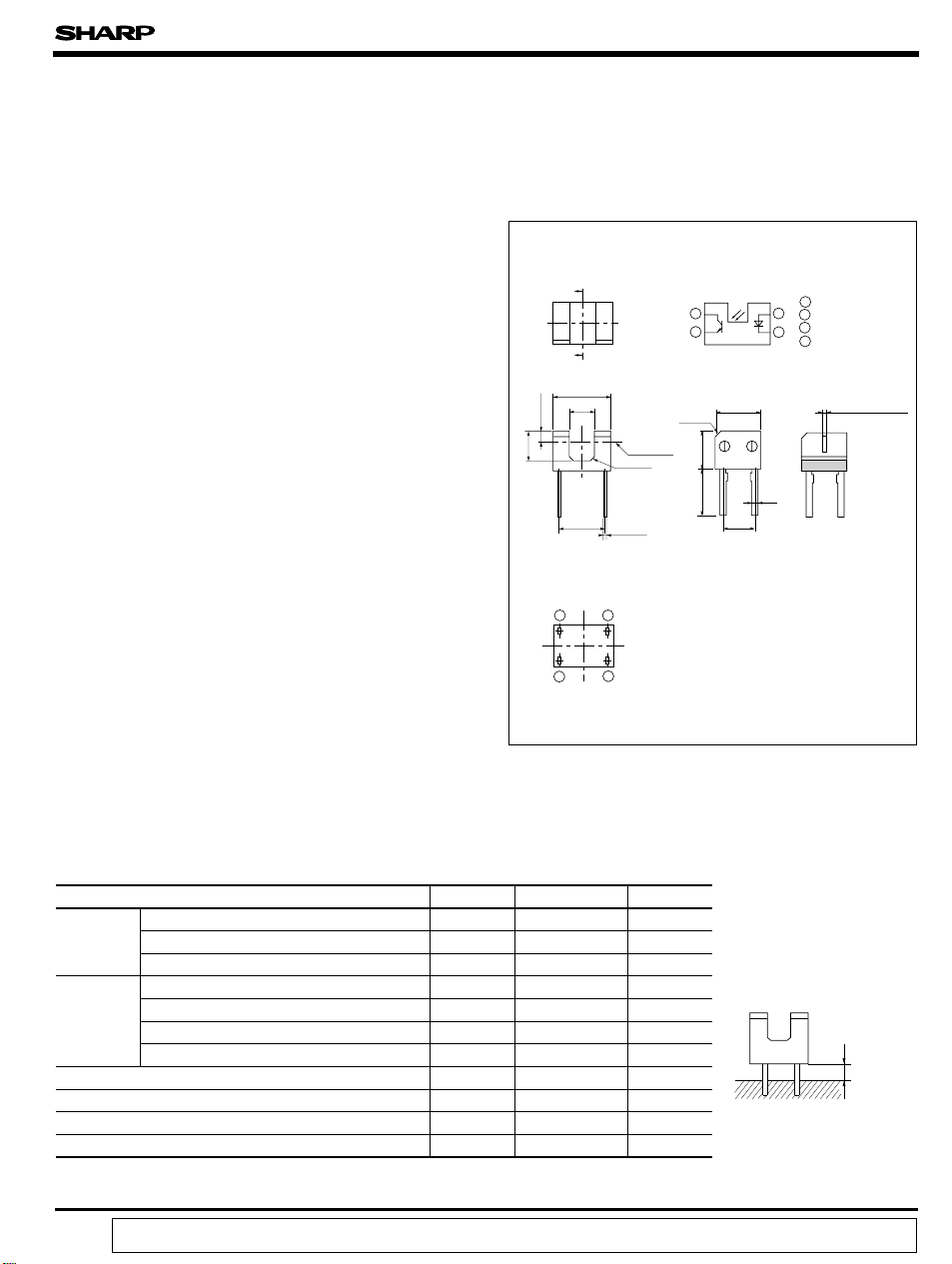
Outline Dimensions
(Unit : mm)
1. Low height type (Height : 3.1 mm)
2. Wide gap type (Gap : 2.0 mm)
3. Detector side slit width : (0.3) mm
■
Applications
1. FDDs
2. Cameras
3. Camera-integral VCRs
Top View
aa
4.5
2.0
(0.85)
2.3
❈ 3.55
3
2
4
1
Internal connection diagram
(C0.4)
Optical
center
(C0.3)
+
0.2
0.15
-
0.1
1 Anode
12
2 Collector
3 Emitter
S
3.4
4 Z
❈ 2.54
0.4
4
4 Cathode
a-a section
(0.3) Slit width
3
3.1
3.6± 0.5
* Tolerance : ± 0.2
* ( ) : Reference dimensions
* The dimensions indicated by ❈ refer
to those measured from the lead base.
■
Absolute Maximum Ratings
(Ta=25˚C)
Parameter Symbol Rating Unit
Forward current
Input
Reverse voltage
Power dissipation
Collector-emitter voltage
Output
Emitter-collector voltage
Collector current
Collector power dissipation
Total power dissipation
Operating temperature
Storage temperature
*1
Soldering temperature
*1 For 5 seconds
“ In the absence of confirmation by device specification sheets, SHARP takes no responsibility for any defects that occur in equipment using any of SHARP's devices, shown in catalogs,
data books, etc. Contact SHARP in order to obtain the latest version of the device specification sheets before using any SHARP's device.”
I
F
V
R
P
V
CEO
V
ECO
I
C
P
C
P
tot
T
opr
T
stg
T
sol
50 mA
6V
75 mW
35 V
6V
20 mA
75 mW
100 mW
-25to+85
- 40 to + 100
˚C
˚C
260 ˚C
Soldering area
1mm or more
GP1S93
■
Electro-optical Characteristics
Parameter Symbol Conditions MIN. TYP. MAX. Unit
Input
Output
Forward voltage
Reverse current
Dark current
Collector current I
Transfer
characteristics
Collector-emitter saturation voltage
Response time
Rise time
Fall time
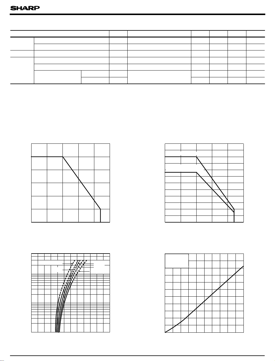
Fig. 1 Forward Current vs. Ambient
Temperature
60
50
)
mA
(
40
F
30
20
Forward current I
10
V
IF= 20mA - 1.2 1.4 V
F
VR=3V - - 10
I
R
I
VI
VCE= 20V - -
CEO
= 5mA, VCE=5V -
I
F
C
)
= 10mA, IC=40µA - - 0.4 V
CE(sat
F
t
r
IC= 0.1mA, VCE= 5V, RL=1kΩ
t
f
Fig. 2 Power Dissipation vs.
Ambient Temperature
120
Total power dissipation
100
Input side power dissipation and
output side collector power dissipation
80
60
40
Power dissipation P (mW)
20
(Ta=25˚C)
-7
1x 10
100 400
- 50 150 µ s
- 50 150 µ s
µA
A
µA
0
- 25 0 25 50 75 100
Ambient temperature Ta (˚C) Ambient temperature Ta (˚C)
500
= 75˚C
T
200
)
100
mA
(
F
Forward current I
a
50˚C
50
20
10
5
2
1
0 0.5 1 1.5 2
Forward voltage VF (V
)
85
25˚C
0˚C
-25˚C
2.5 3
0
- 25 0 25 50 75 100
Fig. 4 Collector Current vs. Forward CurrentFig. 3 Forward Current vs. Forward Voltage
VCE=5V
1.0
Ta =25˚C
)
0.8
mA
(
C
0.6
0.4
Collector current I
0.2
0
048121620
Forward current IF (mA
85
)
 Loading...