

GP1S29
GP1S29
Subminiature Photointerrupter
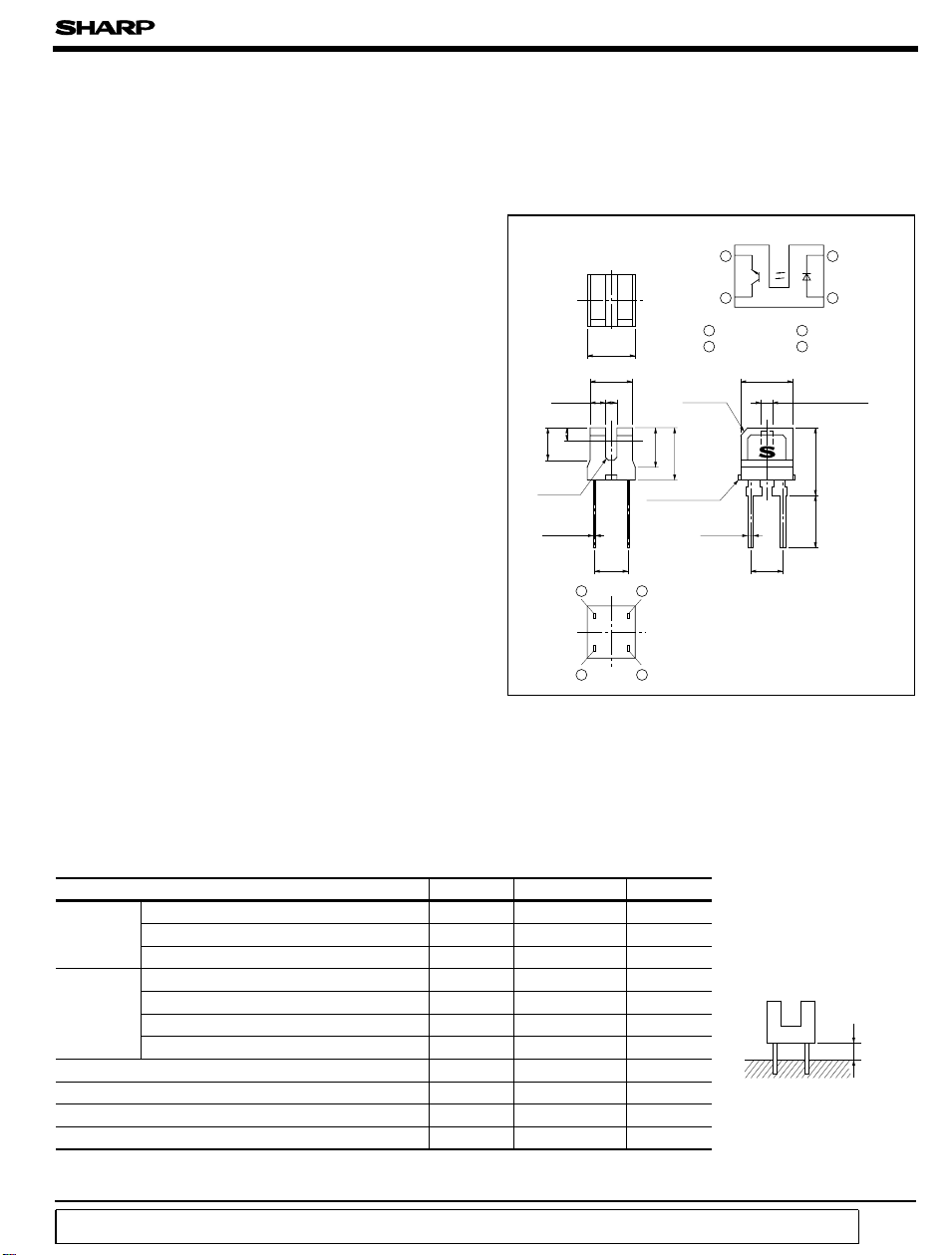
■ Features ■ Outline Dimensions
1. Ultra-compact type
2. Thin detection portion
(Thickness of detection portion: 3.2mm
)
Internal connection diagram
■ Applications
1. Cameras
2. Floppy disk drives
Note) Please use carefully not to
receive external disturbing
light because the back face of
detector element is not covered
with case.
Center of
light path
2.5
(
C0.3
4 - 0.15 4 - 0.4
(
1.15
)
1.0
(
3.6
3.2
)
0.9
)
❈
2.54
4
(
C0.8
3.0
4.0
Rest of gate
(2)
1
* Tolerance:± 0.2mm
* Burr's dimensions: 0.15MAX.
* Rest of gate: 0.3MAX.
* ( ): Reference dimensions
* The dimensions indicated by ❈ refer
23
to those measured from the lead base.
3
4
1 Anode
2 Cathode
)
4.0
❈
2.54
(
Unit : mm
2
1
3 Emitter
4 Collector
(
)
0.8
Slit width
5.1
MIN.
4.0
)
■ Absolute Maximum Ratings
(
Ta= 25˚C
)
Parameter Symbol Rating Unit
Forward current 50 mA
Input
Reverse voltage 6 V
Power dissipation
Collector-emitter voltage 35 V
Output
Emitter-collector voltage 6 V
Collector current 20 mA
Collector power dissipation
Total power dissipation
Operating temperature - 25 to + 85 ˚C
Storage temperature
*1
Soldering temperature
*1 For 5 seconds
“ In the absence of confirmation by device specification sheets, SHARP takes no responsibility for any defects that occur in equipment using any of SHARP's devices, shown in catalogs,
data books, etc. Contact SHARP in order to obtain the latest version of the device specification sheets before using any SHARP's device.”
I
F
V
R
P
V
CEO
V
ECO
I
C
P
C
P
tot
T
opr
T
stg
T
sol
75 mW
75 mW
100 mW
Soldering area
- 40 to + 100 ˚C
260 ˚C
1mm or more
GP1S29
■ Electro-optical Characteristics
Parameter Symbol Conditions MIN. TYP. MAX. Unit
Input
Output Collector dark current I
Transfercharacteristics
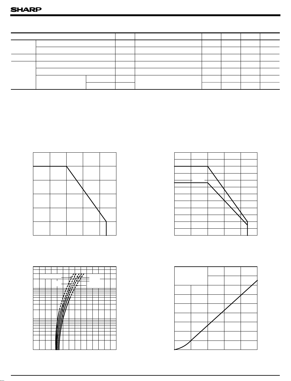
Fig. 1 Forward Current vs. Ambient
Temperature
)
mA
(
F
Forward current I
Forward voltage V
Reverse current I
Collector Current Ic
Collector-emitter saturation voltage
Response time
60
50
40
30
20
10
Rise time
Fall time - 50 150 µ s
(
Ta = 25˚C
F
R
CEO
(
V
sat
CE
t
r
t
f
IF= 20mA - 1.2 1.4 V
VR=3V - - 10 µA
VCE= 20V - - A
I
= 1.5mA, V
F
)
I
= 3mA, I = 30 µ A
FC
V
= 5V, R
CE L
I
= 100µ A
C
CE
=1kΩ
=5V
40 240
- - 0.4 V
- 50 150 µ s
1x10
- µ A
-
7
)
Fig. 2 Power Dissipation vs.
Ambient Temperature
120
P
P, P
tot
c
100
)
mW
80
(
60
40
Power dissipation P
20
0
- 25 0 25 50 75 100
Ambient temperature Ta (˚C
85
)
Fig. 3 Forward Current vs. Forward Voltage
500
Ta= 75˚C
200
)
100
mA
(
50
F
20
10
Forward current I
5
2
1
0 0.5 1 1.5 2
50˚C
Forward voltage VF (V
25˚C
0˚C
-
25˚C
2.5 3
)
3.5
0
- 25 0 25 50 75 100
Ambient temperature Ta (˚C
85
)
Fig. 4 Collector Current vs. Forward Current
1.8
VCE=5V
1.6
1.4
)
mA
1.2
(
C
1.0
0.8
0.6
Collector current I
0.4
0.2
= 25˚C
T
a
0
02
Forward current IF (mA
10468
)
 Loading...