

Page 1
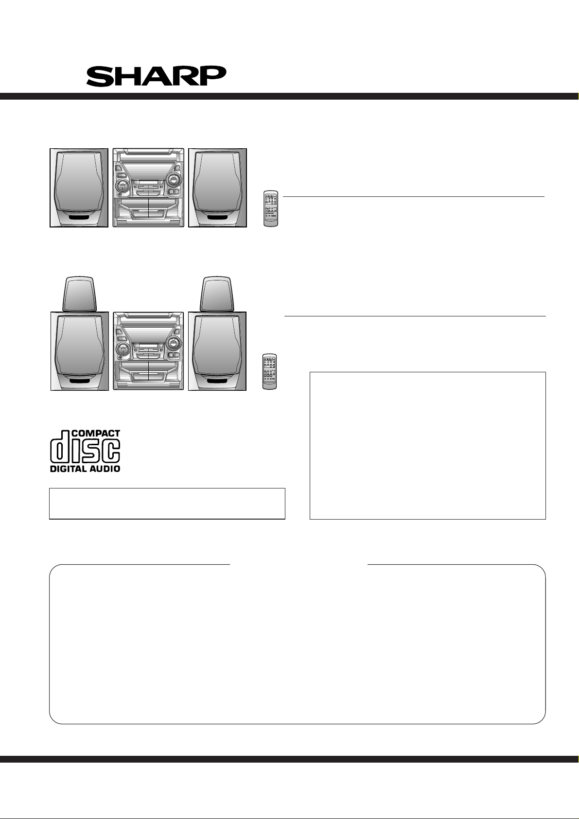
Illustration: CD-BP1300W
CD-BP1300W/BP1350W
SERVICE MANUAL
No. S6055CDP1300W
MINI COMPONENT SYSTEM
MODEL CD-BP1300W
CD-BP1300W Mini Component System consisting of
CD-BP1300W (main unit) and CP-BP1300 (speaker system).
MINI COMPONENT SYSTEM
MODEL CD-BP1350W
CD-BP1350W Mini Component System consisting of
CD-BP1350W (main unit), CP-BP1350 (front speaker) and
GBOXS0043AWM1 (surround speaker).
This Service Manual is for the CD-BP1300W/BP1350W, which is a
minor-modification model of the CD-BP1200W/BP1250W. This
Illustration: CD-BP1350W
• In the interests of user-safety the set should be restored to its
original condition and only parts identical to those specified be
used.
manual, therefore, describes only the changed points from the
service manual. Please refer to the CD-BP1200W/1250W service
manual (No.S6052CDP1200W) together with this manual.
CD-BP1200W/BP1250W
REMOVING AND REINSTALLING THE MAIN PARTS.. 11
ADJUSTMENT................................................................ 12
TROUBLESHOOTING (CD SECTION) .......................... 35
FUNCTION TABLE OF IC .............................................. 39
FL DISPLAY.................................................................... 45
CONTENTS
SAFETY PRECAUTION FOR SERVICE MANUAL ........................................................................................................... 2
VOLTAGE SELECTION..................................................................................................................................................... 2
SPECIFICATIONS ............................................................................................................................................................. 3
NAMES OF PARTS ........................................................................................................................................................... 4
OPERATION MANUAL ...................................................................................................................................................... 6
DISASSEMBLY.................................................................................................................................................................. 8
BLOCK DIAGRAM ........................................................................................................................................................... 11
SCHEMATIC DIAGRAM .................................................................................................................................................. 12
WIRING SIDE OF P.W.BOARD....................................................................................................................................... 22
NOTES ON SCHEMATIC DIAGRAM .............................................................................................................................. 30
TYPES OF TRANSISTOR AND LED................................................................................................................................30
WAVEFORMS OF CD CIRCUIT...................................................................................................................................... 31
VOLTAGE ........................................................................................................................................................................ 32
REPLACEMENT PARTS LIST/EXPLODED VIEW
Page
Page
SHARP CORPORATION
– 1 –
This document has been published to be used
for after sales service only.
The contents are subject to change without notice.
Page 2
CD-BP1300W/BP1350W
SAFETY PRECAUTION FOR SERVICE MANUAL
Precaution to be taken when replacing and servicing the Laser Pickup.
The AEL (Accessible Emission Level) of Laser Power Output for this model is specified to be lower than Class 1 Requirements.
However, the following precautions must be observed during servicing to protect your eyes against exposure to the Laser beam.
(1) When the cabinet has been removed, the power is turned on without a compact disc, and the Pickup is on a position outer than
the lead-in position, the Laser will light for several seconds to detect a disc. Do not look into the Pickup Lens.
(2) The Laser Power Output of the Pickup inside the unit and replacement service parts have already been adjusted prior to shipping.
(3) No adjustment to the Laser Power should be attempted when replacing or servicing the Pickup.
(4) Under no circumstances look directly into the Pickup Lens at any time.
(5) CAUTION - Use of controls or adjustments, or performance of procedures other than those specified herein may result in
hazardous radiation exposure.
CAUTION
This Mini Component System is classified as a CLASS
1 LASER product.
The CLASS 1 LASER PRODUCT label i s located on the
rear cover.
Use of controls, adjustments or performance of procedures other than those specified herein may result in
hazardous radiation exposure.
As the laser beam used in this compact disc player is
harmful to the eyes, do not attempt to disassemble the
cabinet. Refer servicing to qualified personnel only.
Laser Diode Properties
Material: GaAIAs
Wavelength: 780 nm
CAUTION-INVISIBLE LASER RADIATION WHEN OPEN. DO NOT STARE INTO
BEAM OR VIEW DIRECTLY WITH OPTICAL INSTRUMENTS.
VARNING-OSYNLIG LASERSTRALNING NAR DENNA DEL AR OPPNAD. STIRRA
EJ IN I STRALEN OCH BETRAKTA EJ STRALEN MED OPTISKA INSTRUMENT.
ADVERSEL-USYNLIG LASERSTRALING VED ABNING. SE IKKE IND I
STRALEN-HELLER IKKE MED OPTISKE INSTRUMENTER.
VARO! AVATTAESSA OLET ALTTIINA NAKYMATON LASERSATEILYLLE.
ALA TUIJOTA SATEESEEN ALAKA KATSO SITA OPTISEN LAITTEEN LAPI.
VARNING-OSYNLIG LASERSTRALNING NAR DENNA DEL AR OPPNAD.
STIRRA EJ IN I STRALEN OCH BETRAKTA EJ STRALEN GENOM OPTISKT
INSTRUMENT.
ADVERSEL-USYNLIG LASERSTRALING NAR DEKSEL APNES. STIRR IKKE
INN I STRALEN ELLER SE DIREKTE MED OPTISKE INSTRUMENTER.
Emission Duration: continuous
Laser Output: max. 0.6 mW
VOLTAGE SELECTION
Before operating the unit on mains, check the preset voltage. If the voltage is different from your local voltage, adjust the voltage
as follows, Turn the selector with a screwdriver until the appropriate voltage number appears in the window (110 V, 127 V,
220 V or 230 V - 240 V AC).
QACCE0007AW00
QACCA0004AW00
QACCL0002AW00/QACCZ0008AW00
QACCJ0006AW00
Figure 2 AC POWER SUPPLY CORD AND PLUG ADAPTOR
– 2 –
QPLGA0003AWZZ
QPLGA0004AWZZ
Page 3
FOR A COMPLETE DESCRIPTION OF THE OPERATION OF THIS UNIT, PLEASE REFER
TO THE OPERATION MANUAL.
CD-BP1300W/BP1350W
CD-BP1300W/BP1350W
SPECIFICATIONS
General
Power source:
Power
consumption:
Dimensions:
Weight:
AC 110/127/220/230-240 V,
50/60 Hz
47 W
Width; 270 mm (10-5/8")
Height; 300 mm (11-13/16")
Depth; 373 mm (14-1 1/16")
5.2 kg (11.4 lbs .)
Amplifier section (CD-BP1300W)
Output power:
Output terminals:
MPO; 64 W (32 W + 32 W)
(10 % T.H.D.)
RMS; 40 W (20 W + 20 W)
(10 % T.H.D.)
RMS; 28 W (14 W + 14 W)
(0.9 % T.H.D.)
Speakers; 6 ohms
Headphones ; 16 - 50 ohms
(recommended; 32 ohms)
Amplifier section (CD-BP1350W)
Output power:
Output terminals:
MPO; 64 W (32 W + 32 W)
(10 % T.H.D.)
RMS; 40 W (20 W + 20 W)
(10 % T.H.D.)
RMS; 28 W (14 W + 14 W)
(0.9 % T.H.D.)
Front speakers; 8 ohms
Surround speakers; 16 ohms
Headphones; 16 - 50 ohms
(recommended; 32 ohms)
Cassette deck section
Frequency
response:
Signal/noise ratio:
Wow and flutter:
CP-BP1300
Type:
Maximum input
power:
Rated input power:
Impedance:
Dimensions:
Weight:
CP-BP1350
Type:
Maximum input
power:
Rated input power:
Impedance:
Dimensions:
Weight:
50 - 14,000 Hz (Normal tape)
55 dB (TAPE 1, playback)
50 dB (TAPE 2, recording/playback)
0.3 % (WRMS)
2-way [13 cm (5-1/4") woofer and
5 cm (2") t weeter]
40 W
20 W
6 ohms
Width; 220 mm (8-11/16")
Height; 300 mm (11-13/16")
Depth; 217 mm (8-9/16")
2.6 kg (5.7 lbs .)/each
2-way [13 cm (5-1/4") woofer and
5 cm (2") tweeter]
30 W
15 W
8 ohms
Width; 220 mm (8-11/16")
Height; 300 mm (11-13/16")
Depth; 217 mm (8-9/16")
2.6 kg (5.7 lbs.)/each
Compact disc player section
Type:
Signal readout:
D/A converter:
Frequency
response:
Dynamic range:
3-disc multi-play compact disc
player
Non-contact, 3-beam semi-conductor laser pickup
1-bit D/A converter
20 - 20,000 Hz
90 dB (1 kHz)
Tuner section
Frequency range:
FM; 88 - 108 MHz
AM; 531 - 1,602 kHz
GBOXS0043AWM1
Type:
Maximum input
power:
Rated input power:
Impedance:
Dimensions:
Weight:
Specifications for this model are subject to change without
prior notice.
– 3 –
(CD-BP1350W ONLY)
8 cm (3-3/32") full-range speaker
10 W
5 W
16 ohms
Width; 150 mm (6")
Height; 150 mm (6")
Depth; 78 mm (3")
0.4 kg (0.9 lbs.)/each
Page 4
CD-BP1300W/BP1350W
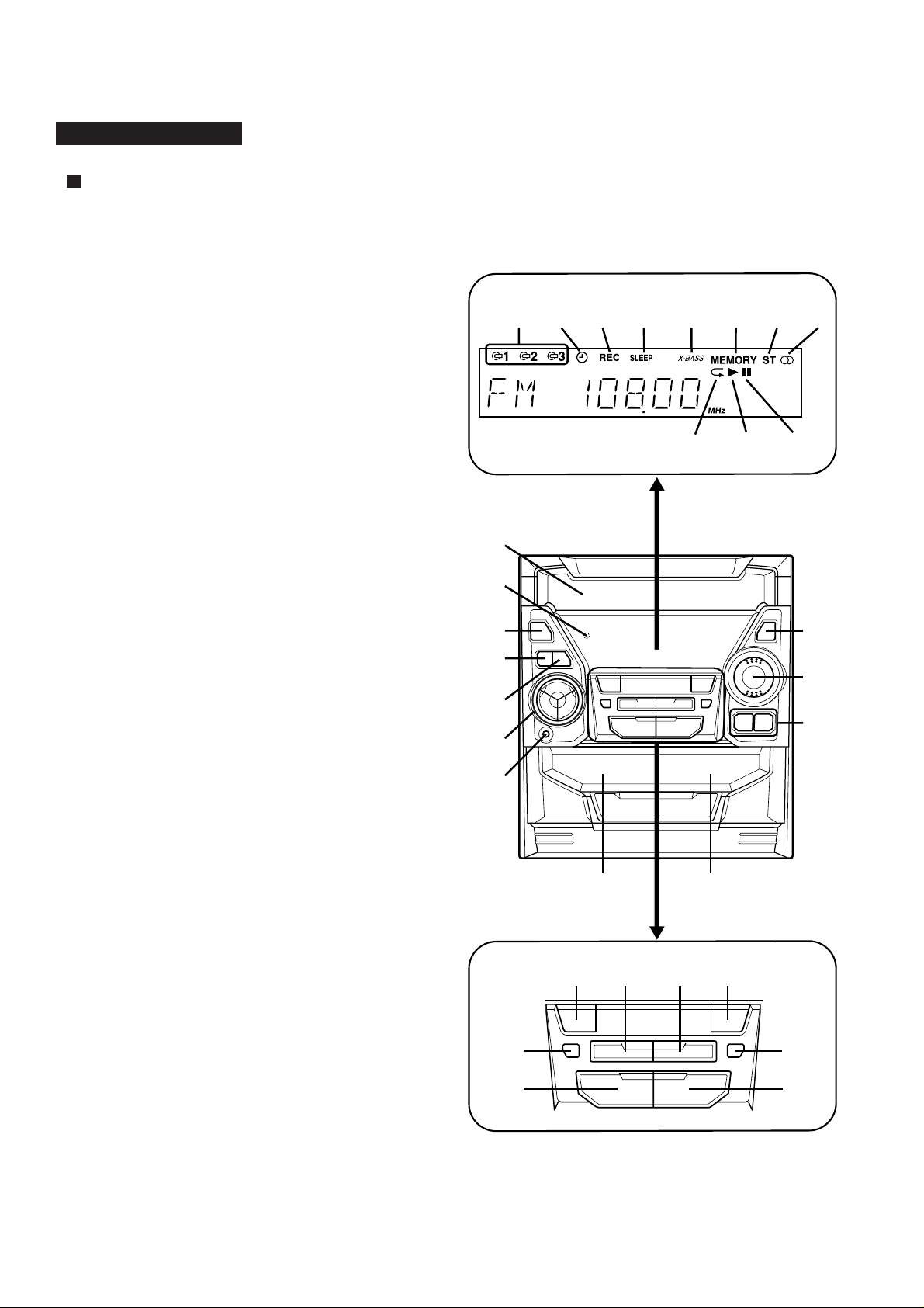
NAMES OF PARTS
CD-BP1300W/BP1350W
Front panel
1.(CD) Disc Number Indicators
2.Timer Indicator
3.Record Indicator
4.Sleep Indicator
5.Extra Bass Indicator
6.(CD/TUNER) Memory Indicator
7.FM Stereo Mode Indicator
8.FM Stereo Indicator
9.(CD) Repeat Indicator
10.(CD/TAPE) Play Indicator
11.(CD) Pause Indicator
12.(CD) Disc Tray
13.Timer Set Indicator
14.On/Stand-by Button
15.Timer/Sleep Button
16.Clock Button
17.Function Selector Buttons
18.Headphone Socket
19.Equalizer Mode Selector/Extra Bass/Demo Mode
Button
20.Volume Up/Down Buttons
21.Tuning and Time Up/Down Buttons
12345678
11109
12
13
22.(TAPE 1) Cassette Compartment
23.(TAPE 2) Cassette Compartment
24.(CD) Disc Skip Button
25.(CD) Track Down/Review Button
(TUNER) Preset Down Button
(TAPE 2) Rewind Button
26.(CD) Track Up/Cue Button
(TUNER) Preset Up Button
(TAPE 2) Fast Forward Button
27.(CD) Open/Close Button
28.Memory/Set Button
29.(CD/TAPE) Stop Button
30.(TAPE 2) Record Pause Button
31.(CD) Play/Repeat Button
(TAPE) Play Button
15
16
17
18
28
24
22
25 26 27
1914
20
21
23
30
– 4 –
29
31
Page 5
CD-BP1300W/BP1350W
Rear panel
3
4
5
1
6
7
2
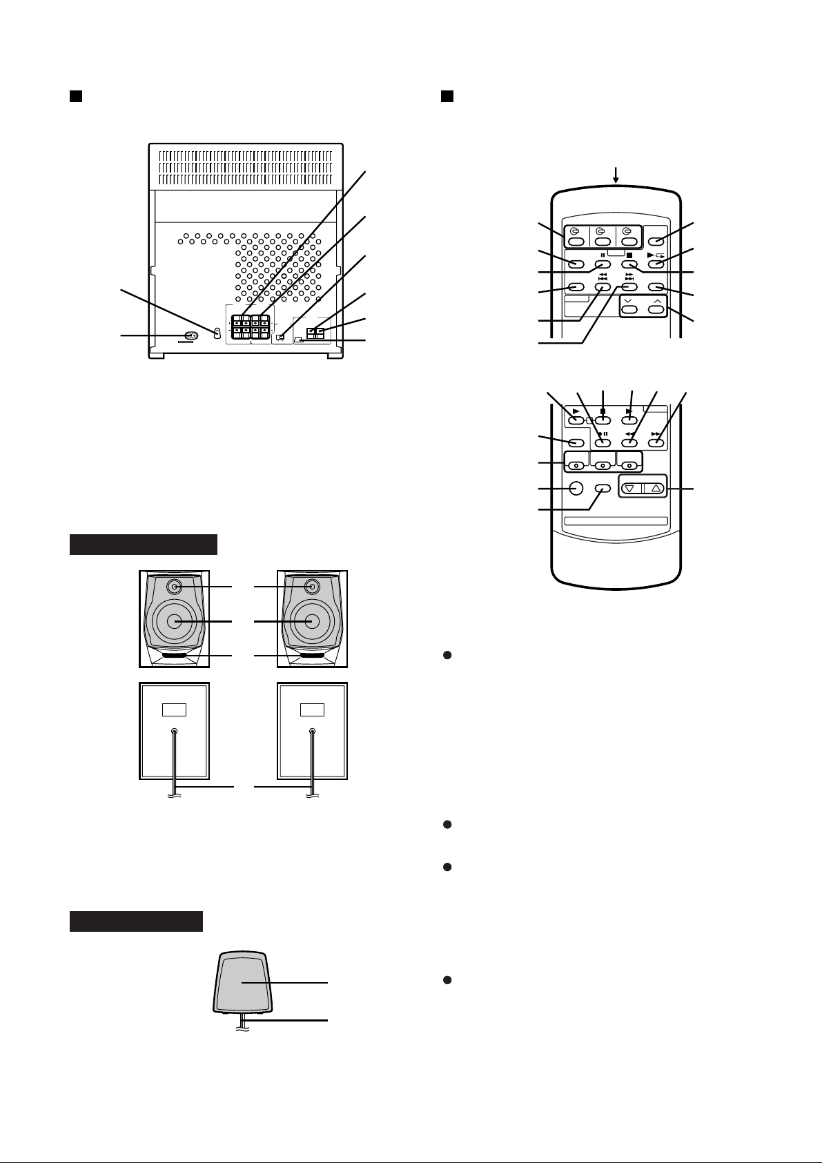
1.AC Voltage Selector
2.AC Power Input Socket
3.Surround Speaker Terminals (CD-BP1350W ONLY)
4.Front Speaker Terminals
5.Span Selector Switch
6.FM Aerial Earth Terminal
7.FM 75 Ohms Aerial Terminal
8.AM Loop Aerial Input Socket
8
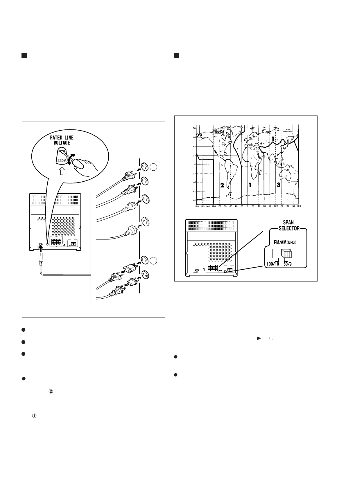
Remote control
2
3
4
5
6
7
19
20
21
22
1
8
9
10
11
12
151413 161718
23
CP-BP1300/BP1350
1.Tweeter
2.Woofer
3.Bass Reflex Duct
4.Speaker Wire
GBOXS0043AWM1
1
2
3
4
(CD-BP1350W ONLY)
1.Remote Control Transmitter LED
CD control section
2.Disc Number Select Buttons
3.Memory Button
4.Pause Button
5.Clear Button
6.Track Down/Review Button
7.Track Up/Cue Button
8.Disc Skip Button
9.Play/Repeat Button
10.Stop Button
11.Random Button
Tuner control section
12.Preset Up/Down Buttons
Tape control section
13.(TAP E 1) Play Button
14.(TAP E 2) Record Pause Button
15.(TAP E 1/2) Stop Button
16.(TAP E 2) Play Button
17.(TAP E 2) Rewind Button
18.(TAP E 2) Fast Forward Button
1.Full-Range Speaker
2.Speaker Wire
1
2
Common section
19.Equalizer Mode Selector Button
20.Function Selector Buttons
21.On/Stand-by Button
22.Extra Bass Button
23.Vo lume Up/Down Buttons
– 5 –
Page 6
CD-BP1300W/BP1350W
g
OPERATION MANUAL
Connecting the AC power lead
Check the setting of the AC voltage selector located on the
rear panel before plugging the unit int o an AC socket. If necessary, adjust the selector to correspond to the AC power
voltage used in your area.
Selector adjustment:
Turn the selector with a screwdriver until the appropriate
voltage number appears in the window (110 V, 127 V, 220 V
or 230 V - 240 V AC).
1
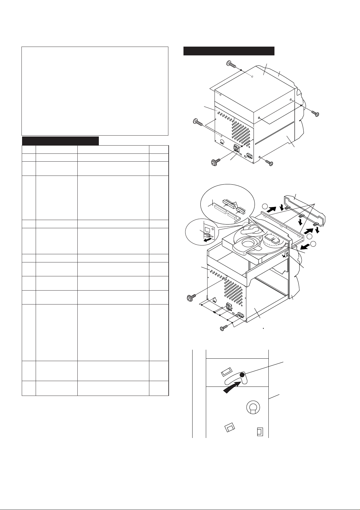
AM/FM interval (span)
The International Telecommunication Union (ITU) has
established that member countries should maintain either a
10 kHz or a 9 kHz inter val between broadcasting frequencies of any AM station. The illustration shows the 9 kHz
interval zones (regions 1 and 3), and the 10 kHz interval
zone (region 2).
Before using the unit, set the SPAN SELECTOR switch (on
the rear panel) to AM tuning interval (span) of your area.
2
To an AC socket
Notes:
Plug the AC power lead into an AC socket, after any connections.
Unplug the AC power lead from the AC socket if the unit
will not be in use for a prolonged period of time.
Never use a power lead other than the one supplied. Use
of a power lead other than the one supplied may cause
an electric shock or fire.
AC Plug Adaptor
In areas (or countries) where an AC socket as shown in
illustration is used, connect the unit using the AC plug
adaptor supplied with the unit, as illustrated. The AC plug
adaptor is not included in areas where the AC wall socket
and AC power plug can be directly connected (see illustration ).
Note for users in Australia and New Zealand:
An AC plug adaptor is not supplied if the lead has an Australian Standard plu
.
To change the tuning zone:
1
Press the ON/STA ND-BY button to enter the standby mode.
2
Set the SPAN S ELECTOR switch to "50/9" for 9 kHz
AM interval (50 kHz FM interval), and "100/10" for 10
kHz AM interval (100 kHz FM interval).
3
Whilst pressing down the / button and the
EQUALIZER/X-BASS/DEMO button, hold down the
ON/STAND-BY button for at least 1 second.
"CLEAR AL" will appear.
Caution:
The operation explained above will erase all data stored
in memory including clock and timer settings, and tuner
and CD presets.
– 6 –
Page 7
CD-BP1300W/BP1350W
SETTING THE CLOCK
In this example, the clock is set for the 24-hour (0:00) sys-
tem.
1
Press the ON/STAND-BY button to enter the stand-
by mode.2Press the CLOCK button.
3
Within 5 seconds, press the MEMORY/SET button.
4
Press the TUNING/TIME ( or ) button to select the
time display mode.
Note that this can only be set when the unit is first
installed or it has been reset.
5
Press the MEMORY/SET button.
6
Press the TUNING/TIME ( or ) button to adjust
the hour.
Press the TUNING/TIME ( or ) button once to
advance the time by 1 hour. Hold it down to advance con-
tinuously.
When the 12-hour display is selected, "AM" will change
automatically to "PM".
7
Press the MEMORY/SET button.
8
Press the TUNING/TIME ( or ) button to adjust
the minutes.
Press the TUNING/TIME ( or ) button once to
advance the time by 1 minute. Hold it down to change the
time in 5-minute intervals.
The hour setting will not advance even if minutes
advance from "59" to "00".
9
Press the MEMORY/SET button.
The clock starts operating from "0" second. (Seconds are
not displayed.) And then the clock display will disappear
after a few seconds.
To see the time display:
Press the CLOCK button.
The time display will appear for about 5 seconds.
Note:
The clock display will flash on and off at the push of the
CLOCK button when the AC power supply is restored
after a power failure occurs or after the AC power lead is
disconnected. If this happens, follow the procedure below
to change the clock time.
To change the clock time:
1 Press the CLOCK button.
2 Within 5 seconds, press the MEMORY/SET button.
3 Perform steps 6 - 9 above.
To change the time display mode:
1 Perform steps 1 - 2 in "RESETTING THE MICROCOM-
PUTER".
2 Perform steps 1 - 9 above.
(Main unit operation)
"0:00" The 24-hour display will appear.
(0:00 - 23:59)
"AM 0:00" The 12-hour display will appear.
(AM 0:00 - PM 11:59)
"AM 12:00" The 12-hour display will appear.
(AM 12:00 - PM 11:59)
ON/
STAND-BY
CLOCK
MEMORY/SET
TUNING/TIME
( )
AM 0:000:00 AM 12:00
Notes concerning use:
Replace the batteries if the operating distance is reduced
or if the operation becomes erratic.
Periodically clean the transmitter LED on the remote con-
trol and the sensor on the main unit with a soft cloth.
Exposing the sensor on the main unit to strong light may
interfere with operation. Change the lighting or the direc-
tion of the unit.
Keep the remote control away from moisture, excessive
heat, shock, and vibrations.
15
15
0.2 m - 6 m
(8" - 20')
RESETTING THE MICROCOMPUTER
Reset the microcomputer under the following condi-
tions:
To erase all of the stored memory contents (clock and
timer settings, and tuner and CD presets).
If the display is not correct.
If the operation is not correct.
1
Press the ON/STAND-BY button to enter the stand-
by mode.2Whilst pressing down the / button and the
EQUALIZER/X-BASS/DEMO button, hold down the
ON/STAND-BY button for at least 1 second.
"CLEAR AL" will appear.
Caution:
The operation explained above will erase all data stored
in memory including clock and timer settings, and tuner
and CD presets.
EQUALIZER
X-BASS/
DEMO
ON/
STAND-BY
– 7 –
Page 8
CD-BP1300W/BP1350W
DISASSEMBLY
Caution on Disassembly
Follow the below-mentioned notes when disassembling
the unit and reassembling it, to keep it safe and ensure
excellent performance:
1. Take cassette tape and compact disc out of the unit.
2. Be sure to remove the power supply plug from the wall
outlet before starting to disassemble the unit.
3. Take off nylon bands or wire holders where they need to
be removed when disassembling the unit. After servicing
the unit, be sure to rearrange the leads where they were
before disassembling.
4. Take sufficient care on static electricity of integrated
circuits and other circuits when servicing.
CD-BP1300W/BP1350W
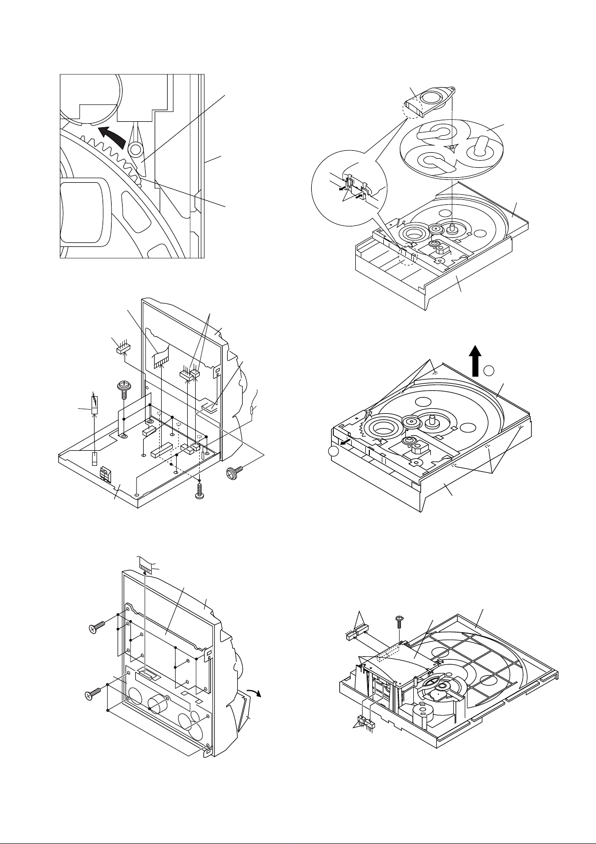
STEP REMOVAL
1 Top Cabinet 1. Screw ..................... (A1) x4 8-1
2 Side Panel 1. Screw ..................... (B1) x2 8-1
(Left/right) 2. Screw ..................... (B2) x2
3 CD Player Unit/ 1. Turn on the power supply, 8-2
CD Tray Cover
2. Screw ..................... (C1) x1
3. Hook....................... (C2) x3
4. Hook....................... (C3) x2
5. Socket .................... (C4) x2
4 Rear Panel 1. Screw ..................... (D1) x8 8-2
5
Main/Headphones 1. Screw........................
PWB 2. Socket .................... (E2) x4
6 Front Panel 1. Screw ..................... (F1) x3 9-2
7 Display PWB 1. Screw .....................
8 Tape Mechanism 1. Open the cassette holder. 9-3
9 Turntable 1. Hook....................... (J1) x2 9-4
10 Disc Tray 1.
11 CD Servo PWB 1. Screw ..................... (L1) x1 9-6
(Note 2) 2. Hook ....................... (L2) x3
12 CD Mechanism 1. Hook....................... (M1) x2 10-1
3. Flat Cable .............. (E3) x1
4. Lug Wire................. (E4) x1
2. Flat Cable .............. (G2) x1
2. Screw...................... (H1) x5
2. Cover ..................... (J2) x1
arrow direction.
2.
3.
3. Socket .................... (L3) x4
2. Hook....................... (M2) x3
Note 1:
How to open the changer manually. (Fig. 8-3)
1. In this state, turn fully the lock lever in the arrow direction
through the hole on the loading chassis bottom.
2.
While holding the lock lever, rotate the cam gear anti clockwise
until the cam gear rib engages with the clamp lever.
3. After that, push forward the CD slide holder.
Note 2:
1. After removing the connector for the optical pickup from the
connector, wrap the conductive aluminium foil around the
front end of the connector to protect the optical pickup from
electrostatic damage.
PROCEDURE
open the disc tray, take out the
CD cover, and close. (Note 1)
(E1) x8 9-2
(G1) x9
Turn fully the lock lever in the
While holding the lock lever, rotate
the cam gear until the cam gear
rib engages with the clamp lever.
Push the slide holder backward to
engage the claw with the groove
and remove it in the direction
of the arrow. ..............
(K1) x6
FIGURE
9-3
8-3
9-1
9-5
(Fig. 9-1)
CD-BP1300W/BP1350W
Top Cabinet
Front Panel
(A1)x2
ø3x12mm
Side Panel
(Left)
(B2)x1
ø3x10mm
CD Tray Cover
(C2) x3
1
1
2
CD Player
Unit
(C3)x1
Front Panel
Main PWB
Side Panel
(Right)
(B2)x1
ø3x10mm
(C3) x1
Pull
Rear
Panel
(C1)x1
ø3x12mm
(A1)x2
ø3x12mm
(B1)x2
ø3x12mm
CD Servo
PWB
Rear
Panel
(C4)x2
(D1)x8
ø3x8mm
Figure 8-1
Figure 8-2
Lock Lever
CD Player Unit
(Bottom View)
Figure 8-3
Note 3:
1. Be careful not to break the claw of the CD mechanism.
2. When fining back the cam gear assembly, let it lock by front
movement.
– 8 –
Page 9
(L3) x2
(L2) x3
(L3) x2
CD Servo
PWB
Slide Chassis
(L1)x1
ø3x8mm
Clamp Lever
CD Player Unit
(Top View)
CD-BP1300W/BP1350W
(J2) x1
Turntable
(E2)x1
(E3)x1
(E2)x1
(E1)x7
ø3x10mm
Main PWB
Figure 9-1
(F1)x3
ø3x8mm
Cam Gear Rib
(E2)x2
Front Panel
(E1)x1
ø3x10mm
Headphones
PWB
(E4)x1
(J1) x2
1
Slide Chassis
Loading Chassis
Figure 9-4
(K1) x3
2
Slide Chassis
(K1) x3
Loading Chassis
(G1)x9
ø3x10mm
Tape
Mechanism
(H1)x5
ø3x10mm
Figure 9-2
(G2)x1
Display PWB
Figure 9-3
Figure 9-5
Front Panel
Open
Cassette
Holder
Figure 9-6
– 9 –
Page 10
CD-BP1300W/BP1350W
CD
Mechanism
(M1) x1
(M2) x3
(M1) x1
Slide Chassis
Figure 10-1
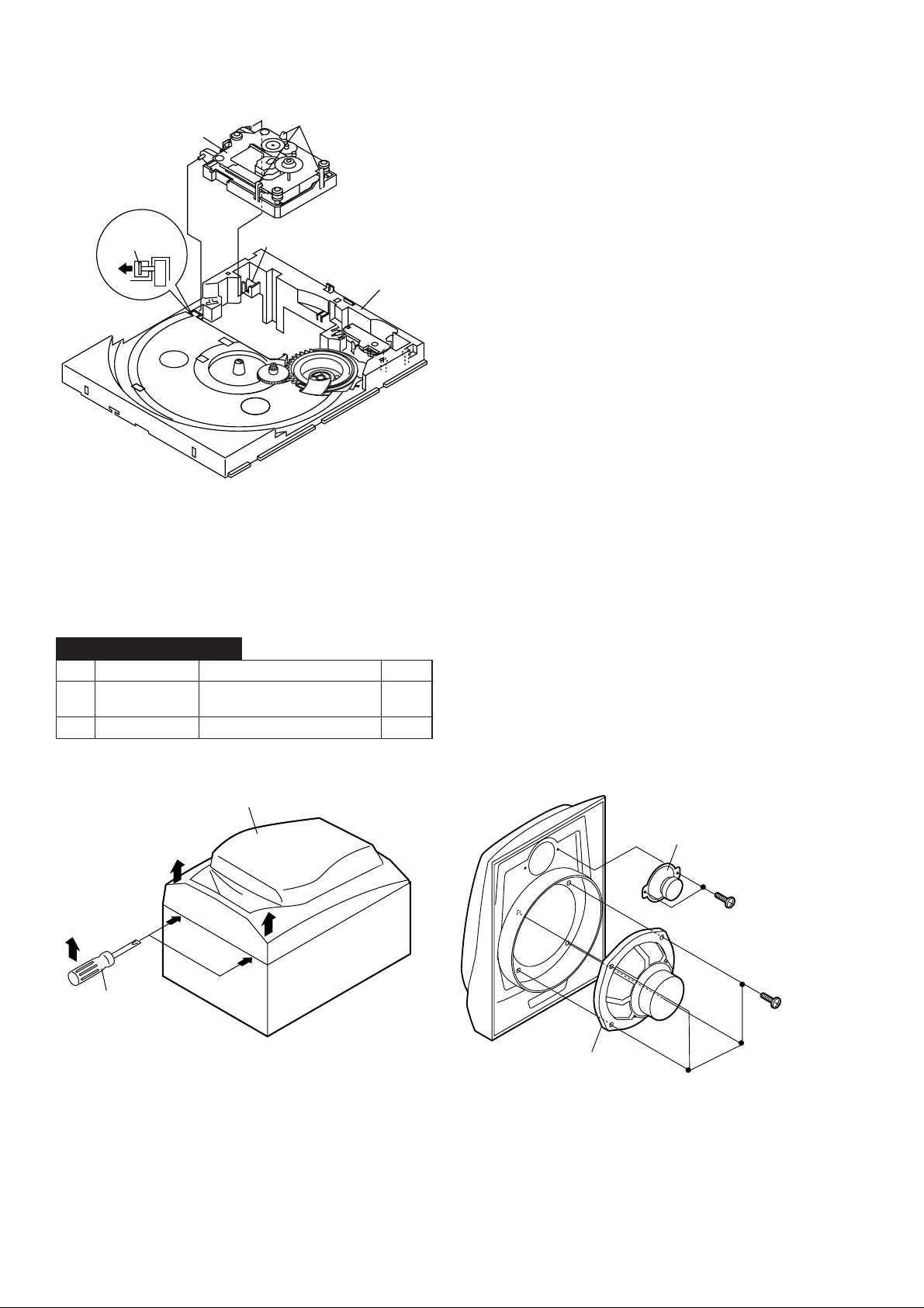
CP-BP1300/BP1350
STEP REMOVAL
1 Woofer 1. Front Panel ............ (A1) x1 10-2
2. Screw ..................... (A2) x4
2 Tweeter 1. Screw ..................... (B1) x2 10-3
Screwdriver
Driver should be
pried away from
speaker box.
PROCEDURE
(A1x1)
FIGURE
Tweeter
(B1)x2
ø3x10mm
(A2)x4
ø4x12mm
Woofer
Figure 10-2
Figure 10-3
– 10 –
Page 11
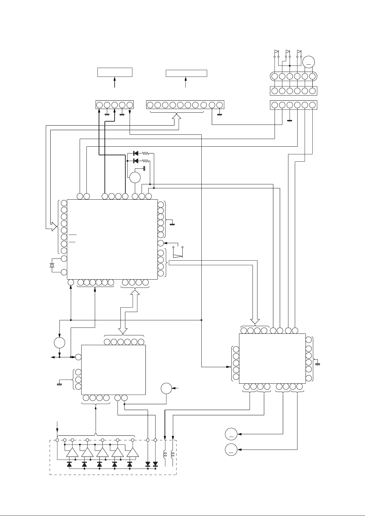
TO MAIN SECTION
(TO IC601)
TO DISPLAY SECTION
CD-BP1300W/BP1350W
SW3
SW2
DISC
CLAMP
3
NUMBER
+
5
4
M
UP/DOWN
MOTOR
-
6
T/T
M3
BI4
SW1
OPEN/
CLOSE
12
XL1
16.9344MHz
R-CH
L-CH
AGND
DGND
2
1
3
4
75
76
65
CE
CL
66
DI
67
DO
68
INT
69
WRQ
70
RES
71
72
DEF
XOUT
52
XIN
51
VDD5V
735183644 49 50 7 14 15 16
CONT7
CONT6
SERVO/SIGNAL
VVDD
ADAVDD
VDD
45 46
LVSS
LCHO
IC2
LC78641E
CONTROL
LVDD
RVDD
XVDD
47 48 32 31
RVSS
RCHO
HFL
+5V(+B3)
5
Q2
CONT4
RFEV
CNP11
CONT3
CONT5
FE
CDINT
30
CONT2
SLD0
SPD0
FD0
TD0
TE
CE
DO
5
43
SW4
PICKUP IN
DI
CLK
6
DRF
WRQ
217
74
64
40
19
13
3
33
26
25
24
23
CLAMP SW
CD RES
89
12
GND
10
CNP12
12
56
3
4
3
4
56
CNS4
CNP4
CONSTANT
VOLTAGE
+3.3V
PICKUP UNIT
+5V
Q1
+5V
30
23
11
9
FIN1
12
+3.3V
FIN2
18 19 20
17
TE
TE-
HFL
IC1
LA9235M
SERVO AMP.
PD
TIN2
TIN1
7
34
8
FE
LDD
1
2 1725 4142 3839
22
21
VCC1
+5V
18
VCC4
40
24
VCC2
23
VCC3
28
M63001FP
FOCUS/TRACKING/
SPIN/SLED DRIVER
45671516 26 27
M
M
IC3
FE-
RFEV
LASER
DRIVER
Q3
FOCUS COIL
TRACKING COIL
+3.3V
M2
SLED
MOTOR
M1
SPINDLE
MOTOR
35
29
22
21
14
8
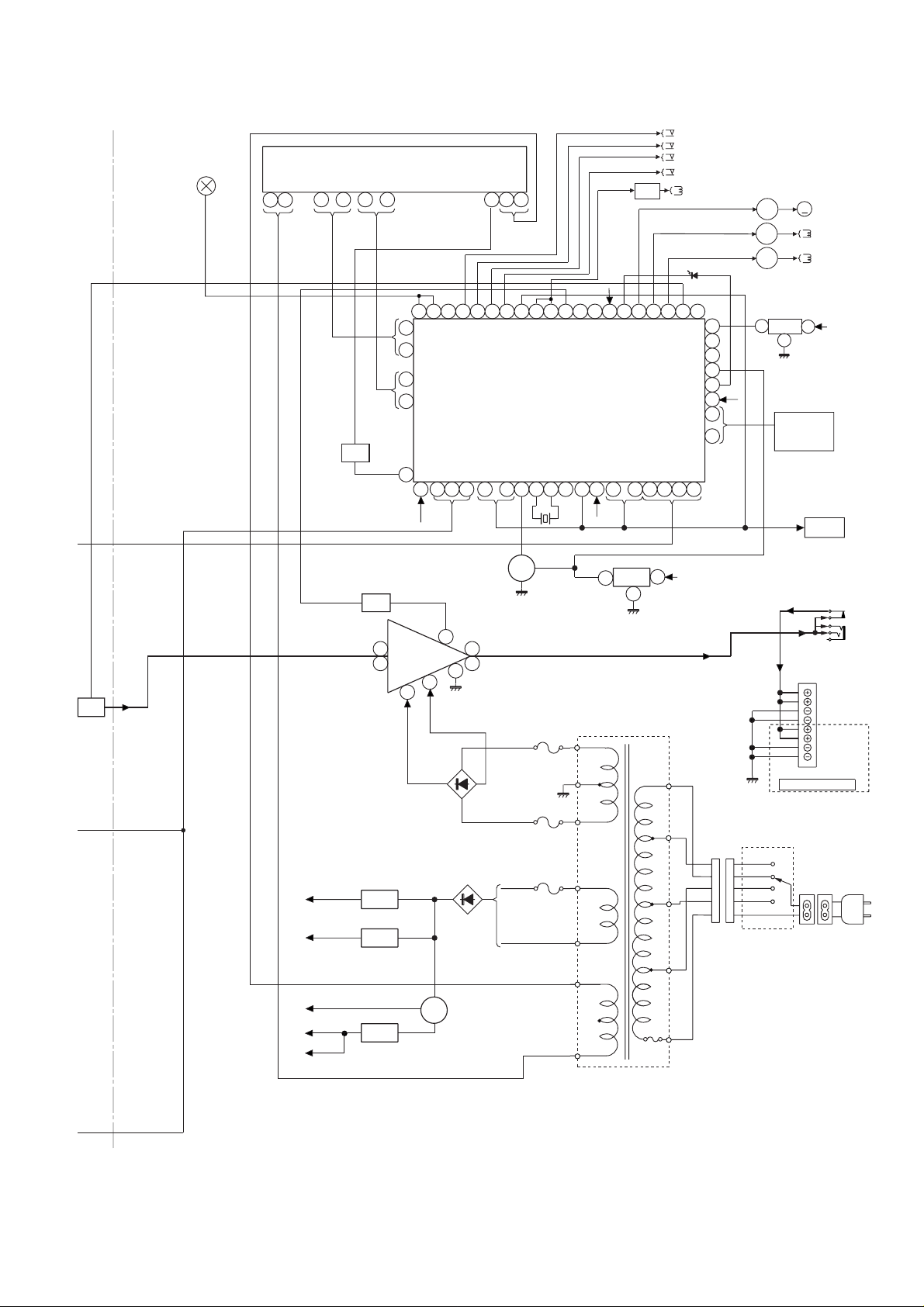
Figure 11 BLOCK DIAGRAM (1/3)
– 11 –
Page 12
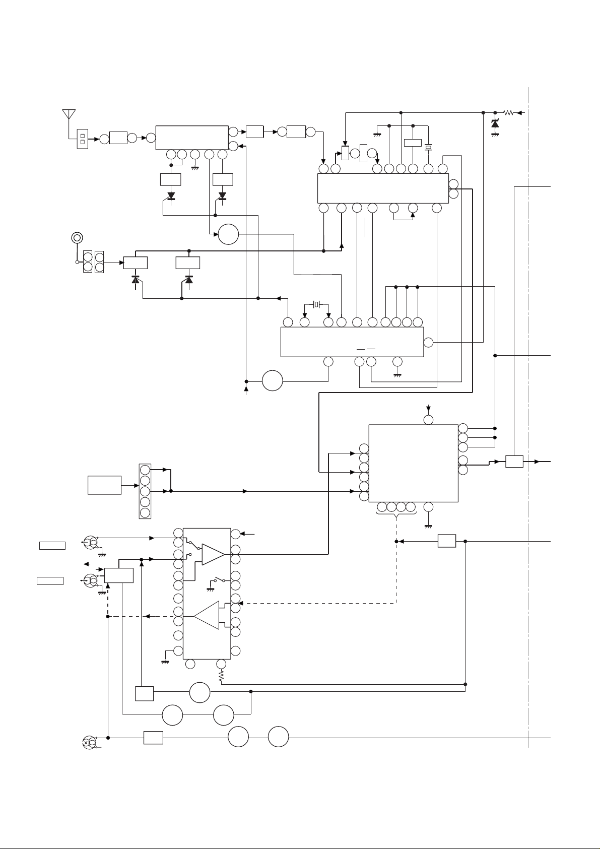
CD-BP1300W/BP1350W
FM ANTENNA
TERMINAL
SO302
AM LOOP
ANTENNA
1
2
1
CNP302
1
2
BF301
3
T303
1
FM FRONT END
3
FM
L312
RF
AM
TRACKING
IC301
TA7358AP
4
5
T306
8
7
FM
OSC
T301
AM BAND
COVERAGE
Q302
6
9
FM +B
T302
1
FM OSC
VT
SWITCHING
Q360
CF303
20
4.5MHZ
1
PLL(TUNER)
FM
3
FM MPX. /AM IF
23
AM OSC IN
X352
22
IC302
LC72131
7
21
AM MIX
IC303
LA1832S
FM IFDET/
21
AM RF IN
16
1
T351
24
AM OSC OUT
15
FM/AM
9
3
CF352
AM IF
7
STEREO
11
MO/ST
10
+B2
X351
CF351
5
4
9
FM+B
GND
FM/AM
OUT
18
CLK
DI
CE
4
5
3
8
FM
DET
16
VDD
13
1 7
MO/ST
VCO
L
14
R
15
FM/AMMPX IN
12
DO
6
17
21
PLAYBACK
HEAD
TAPE 1
REC
PLAYBACK
HEAD
TAPE 2
L-CH
R-CH
L-CH
R-CH
FROM CD
SECTION
CNP11
REC
P.B.
AC BIAS
SWITCHING
Q104~
Q107
CNS601
1
2
3
4
5
REDUCE
SWITCHING
Q108
Q109
R
L
IC101
AN7345K
PLAYBACK AND RECORD/
PLAYBACK AMP.
L(T1)
1
R(T1)
24
L(T2)
2
R(T2)
23
L NF
3
R NF
22
POP
T1/T2
6
L REC
9
REF
16
14
12
REC
NOR/
R REC
15
SWITCHING
Q103
P.B
13
4
21
+B2
L
10
TAPE
R
15
AUDIO PROCESSOR
L
11
TUNER
R
14
L
12
CD
R
13
7
8
+B2
L
PB
R
IC601
LC75341
18
17
+B2
23
3
CLK
MUTING
Q110
Q111
DI
1
CE
24
21
2
R
L
4
SYSTEM
MUTE
Q601
Q602
REC/PLAY
5
20
H/N
RECRL
7
18
L NF
8
R NF
17
ALC
10
T1/T2 HIGH
19
ERASE
HEAD
BIAS
OSC
Q114
L104
Q101
SWITCHING
Q102
Q112
SWITCHING
BIAS
Q113
Figure 12 BLOCK DIAGRAM (2/3)
– 12 –
BAIS
Page 13
+B2
SW802
SPAN SELETOR
CD-BP1300W/BP1350W
R. PLAY
F. PLAY
Q702
Q703
212322
T2 PLAY
T1 PLAY
SYS. STOP
AVDD
CEDICL
SOLENOID
LED722
40
39
38
37
36
35
34
33
~
31
DO
24
+B4
MOTOR
DRIVER
Q706
Q705
Q704
1
RX701
TAPE
MOTOR
M
3
+B
2
KEY
SW701-SW703
SW709-SW721
SW723-SW725
FL701
FL DISPLAY
~~
11
30
21
10
4
60
59575655545352
71
333231
5051
49484746 44434241
+B5
45
VDD
78
IC701
IX0337AW
SYSTEM
MICROCOMPUTER
RESET
~
11
10
12139
1516
VDD
17
20
~
Q701
80
~~
99
100
VDD
41
65
7
SYSTEM
MUTE
Q601
Q602
REC/PLAY
+B2
+B3
SP. DET.
A10V
+5VCD
Q901
Q902
IC901
R
STK40202
15
POWER AMP.
L
1
+Vcc
KIA7810AP
VOLTAGE
REGULATOR
IC801
IC802
KIA7805P
VOLTAGE
REGULATOR
+B5
8
+B1
9
3
13
-B1
D814
D810-D812
10
7
R-OUT
L-OUT
XL701
4.1943MHz
Q707
F803
T3.15A L 250V
F802
T3.15A L 250V
F801
T2A L 250V
+B5
IC704
PT801
1
+B5
2
3
KIA7042AP
RESET
POWER TRANSFORMER
HEADPHONES
SO901
SPEAKER
TERMINAL
CD-BP1350W ONLY
SW801
VOLTAGE SELECTOR
220V
230-240V
110V
127V
TO CD
SECTION
JK901
FRONT
SPEAKER
SURROUND
SPEAKER
SO801
AC INPUT
SOCKET
AC POWER
SUPPLY CORD
AC 110/127/220/
230-240V, 50/60Hz
BAIS
+B4
+B5
+B6
M_10V
UN SW 5V
SW 5V
IC803
AN78L05
CONSTANT
VOLTAGE REGULATOR
Figure 13 BLOCK DIAGRAM (3/3)
Q805
T.F.
– 13 –
Page 14
CD-BP1300W/BP1350W
R
.
0
R
6
1
2
A
CD SERVO PWB-B
C54
47/10
R55
68K
+B
TIN1
FIN1
FIN2
TIN2
C7
10/16
+B
R50
47
C23
0.047
IC1
LA9235M
FIN1
FIN2
0.022
TIN1
TIN2
C6
100/6.3
REF1
VREF
C8
LDD
GND
LDON
AGON
EFBL
TEST0
TES1
C55
0.01
R25
10K
SERVO AMP.
REF
AGCON
PH/BH
30
ODRV
29
28
REF
PH
27
26
25
DH
24
23
22
REF
21
LPF
20
REF
LPF
19
REF
18
17
16
1
REF
2
REF
3
REF
4
REF
5
REF
6
7
APC
8
9
10
ODRV
11
AGCON
12
13
14
15
ODRV
REF
REF
REF
REF
LPF
REF
VCC
RFSW
120K
RF-
RF
NC
PH
BH
RFEV
FEFE
TETE
HFL
TEST
C11
0.47/6.3
C12
0.022
R42
C18
R7
3P
6.8K
(CH)
R6
R5
27K
39K
5
C13
0.01
C14
0.33
R3
47K
R4
10K
R10
27K
C20
0.1
R8
330
C17
0.0047
C42
68P
(CH)
C82
0.022
4
D93
DS1SS133
C25
0.022
C41
100/6.3
C24
2.2/50
C22
100P
R15
10K
1
C
R
1
R80
1M
C26
0.047
C28
47/10
EFBL
CNS1A
CNS1B
Vcc
7
7
7
Vref
6
E
B
5
A
4
B
3
F
2
C
1
7
6
6
6
5
4
3
2
1
R51 68K
5
5
R52 68K
4
4
R53 68K
3
3
R54 68K
2
2
1
1
CNP1
R56
68K
C
+B
C51
C53
47/10
0.001
R47
D
Q3
KTA1266GR
LASER DRIVER
3.3
E
F
ACTUATOR
PICKUP UNIT
G
CD MOTOR PWB-C
SPINDLE
MOTOR
SLED
MOTOR
PICKUP IN
H
SW4
13
C52
0.01
+B
TDO
TR+
FO+
FOTR-
M1
M2
TRTR+
FO+
FOGND
+
M
+
M
-
PD
VR
LD
CNP3A
1
1
2
2
3
3
4
4
5
5
6
6
7
7
CNS2B
CNS3B
6
6
5
5
4
4
3
3
2
1
1
1
2
3
4
5
6
7
88
CNS2A
CNS3A
6
5
4
3
22
1
TR-
1
TR+
2
FO+
3
FO-
4
GND
5
PD
6
VR
7
LD
88
CNP2
+B
R48
6.8K
100/6.3
SP-
6
SP+
5
SL+
4
SL-
3
PUIN
2
GND(D)
1
CNP3
+B
TO
FDO
FD
FO
C46
0.022
FO+
FO-
TR+
TR-
GND
SL-
SL+
SLDO
VCC1
STANDBY
Vref
MUTE
C50
C49
100/6.3
-
1
2
3
4
5
6
7
8
9
10
11
12
13
14
15
16
17
18
19
20
21
-
+
+
-
-
+
+
IC3
M63001FP
FOCUS/TRACKING/
-
-
+
+
+
-
SPIN/SLED DRIVER
+B
+
-
-
+
+
-
LD_M+
42
+
LD_M-
-
41
VCC4
+
40
-
LOADING M+
39
LOADING M-
38
37
36
35
34
33
GND
32
31
30
29
VCC3
28
SP-
27
SP+
26
SPO
-
25
+
VCC2(SPN)
+
24
-
23
+
-
22
SPDO
C47
100/6.3
+B
+B
• NOTES ON SCHEMATIC DIAGRAM can be found on page 30.
1
23456
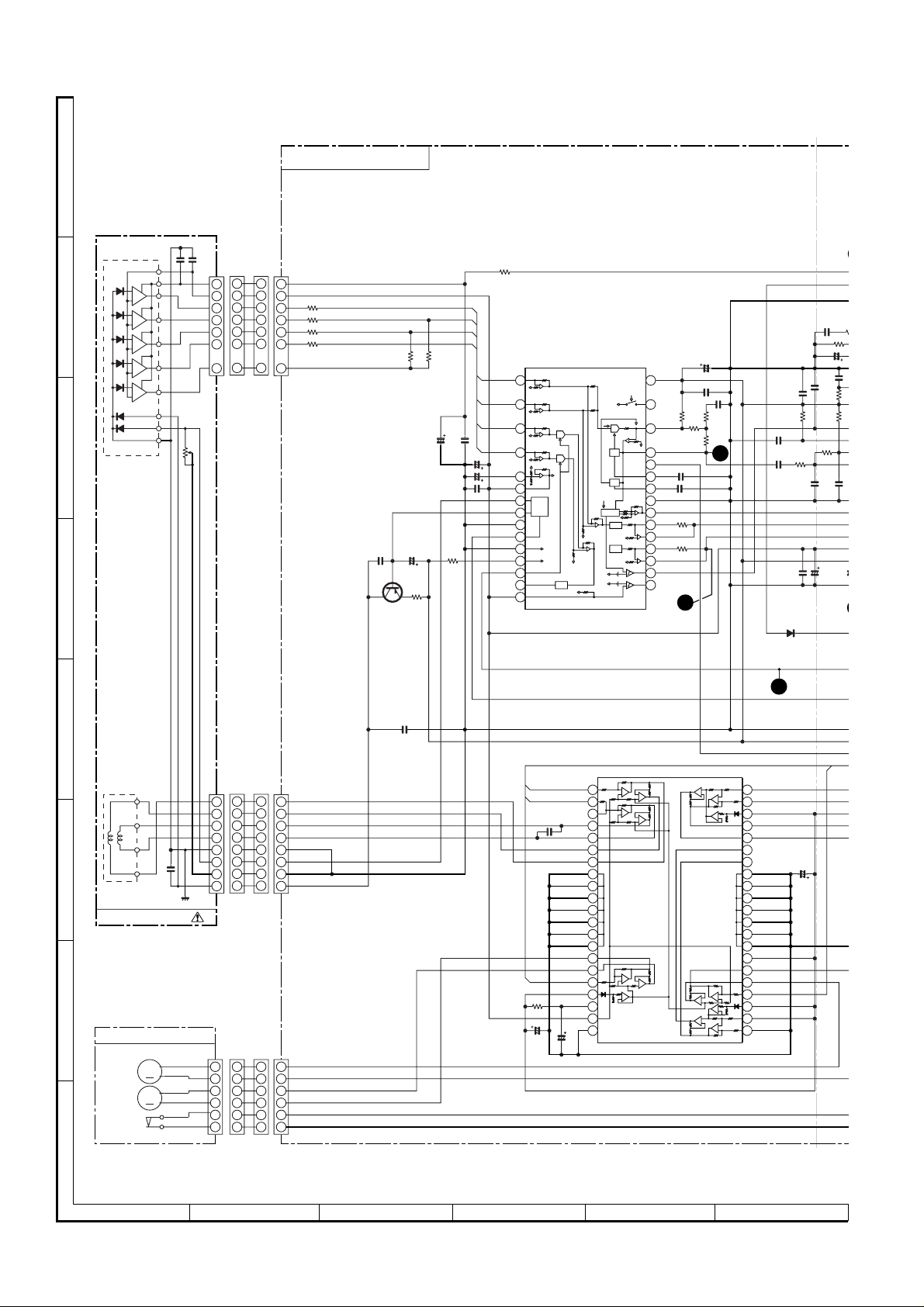
Figure 14 SCHEMATIC DIAGRAM (1/10)
– 14 –
Page 15

CD-BP1300W/BP1350W
R10
27K
C20
0.1
17
047
C82
0.022
D93
S1SS133
3
G M+
G M-
R8
330
C42
68P
(CH)
C47
100/6.3
C25
100/6.3
0.022
C41
+B
C23
0.047
C24
2.2/50
C22
100P
R15
10K
CD SIGNAL
R94
10K
R95
DEFECT
EFMO
JITER
DEFECT
CONTROL
A/DSW
D/A
SLDO
R39
470
+B
80
FG(D_Vref)
+B
R22
470
Q2
KRC102M
10K
FSEQ
79 78
FRAME SYNC
DEFECT,PROTECT
EFM DECODE
CLV
CONTROL
SW
AUTO
ADJUST
LASER
27
28
+B
D22
DS1SS133
1
8
7
R12
680
PD01
R13
680
C81
0.022
PCKIST
R14
1.2K
SLCIST
EFMIN
0.1
PH(RFENV)
ADAVDD
C29
0.022
ADAVSS
PHREF
BHREF
R44
1K
TDO
FDO
PD02
VVSS
VVDD
SLCO
JITTV
JITTC
VREF
TBLO
TDO
FDO
R35
1K
1
2
3
PLL
VCEC
4
5
FR
6
HFL
7
8
SLICE
LEVEL
9
CONTROL
10
11
12
BH
13
14
FE
15
TE
16
17
18
+
-
19
20
21
S/H
22
23
24
26
25
SPDO
1
R38
270
SLDO
SPDO
6
R21
470
D21
DS1SS133
R79
1.5M
C21
0.1
R11
12K
R80
1M
C27
C26
0.047
C28
47/10
2
EFBL
DISC_NO
CONT7
V/vP
77
76
GENERAL
PROCESSEROR
CONT2
CONT1
30
29
R40 1.2K
32
O/C
R67 1K
R68 1K
CONT6
VSS
74
75
SERVO
GENERAL
CONT4
CONT3
32
31
R46 1K
R45 1.2K
C71 100P
C72 0.01
C73 100P
C74 100P
C75 100P
C76 100P
C77 100P
C78 100P
+B
C80
0.022
VDD5V
73
SERVO/SIGNAL
CORRECT
CONT5
33
35
34
PCK
R17 1K
+B
R16
10K
DEF
RES
72
71
IC2
LC78641E
CONTROL
ERROR
AUDIO
OUT
37
36
VDD
C2F
DOUT
100/6.3
WRQ
70
69 68
INTERPOLATION
MUTE
ATTENUATION
DEEMPHASIS
FSX
39
38
C30
0.022
C31
SERIAL
EXTERNAL
DIGITAL
1BIT
COMMAND
INTERFACE
OUT
AUDIO IN
FILTER
DAC
EFLG
40
DIDOINT
67
TEST
CL
66
SUBCODE
DECODE
CRC
9
CE
65
CLOCK
GENERATOR
LPF
R71 1K
R72 1K
R73 1K
R74 1K
R75 1K
R76 1K
R77 1K
R78 1K
L62
2.2µH
64
63
62
61
60
59
58
57
56
55
54
53
52
51
50
49
48
47
46
45
44
43
42
41
+B
SBCK
PW
SBSY
SFSY
16M
DATA
DATACK
LRSY
ASDFIN
ASDACK
ASLRCK
XVSS
XOUT
XIN
XVDD
RVDD
RCHO
RVSS
LVSS
LCHO
LVDD
MUTER
MUTEL
EMPH
L61
0.82µH
16.9344MHz
R20
220
+B
+B
C38
10/16
C39
+B
10/16
47
R19
+B
CONSTANT VOLTAGE
Q1
KTC3203 Y
+B
ZD61
DZ3.9BSB
C34
0.022
R82
2.2K
R81
2.2K
C44
0.022
C45
100/6.3
12
11
10
XL1
330/6.3
DRF
RES
WRQ
INT
DO
DI
CL
CE
+B
R-CH
1
+B
AGND
DGND
INT
WRQ
DRF
CE
DO
DI
CL
RES
L-CH
+B
2
P18 1-A
CNS601
3
FROM MAIN PWB
4
+5V
5
CNP11
CDINT
1
WRQ
2
DRF
3
CE
CNP12
4
5
6
7
8
9
10
P17 12-B
DO
CNS702
DI
FROM DISPLAY PWB
CLK
CD RES
CLAMP SW
GND
C40
10K
R84
0.0015
C43
10K
R83
0.0015
C56
C83
0.022
+B
220
R58
C64
0.47/6.3
+B
3
DO
PN)
+B
+B
• The numbers 1 to 13 are waveform numbers shown in page 31.
7
8 9 10 11 12
Figure 15 SCHEMATIC DIAGRAM (2/10)
– 15 –
GND(D)
DISC_NO
CNS4
O/C
M+
M-
CNP4
BI4
1
1
1
2
2
2
3
3
3
4
4
4
5665
5
6
SW1
OPEN/
CLOSE
SW2
CLAMP
SW3
DISC
NUMBER
+
M3
M
T/T
-
UP/DOWN
LOADING
CD LOADING
MOTOR PWB-E
Page 16

CD-BP1300W/BP1350W
F
0
0
0
0
0
0
0
0
0
9
Q
C
A
B
C708
1/50
R743
FL701
F
F
2
C705
100/10
33
P16
P15
3 4 517 8 96
P14
P20
P13
FL DISPLAY
P11
12 13 14 1511 17 18 1910 16
P18
P19
P12P18GP2P37G6GP4P55GP6P7P8P9P10
22 23 24 2521 27 28 2920 26 30 32331
F9G4G3G2G1GP17
KR
2
1
82 83 84 8581 87 88 8986 90 92 93 94 9591 97 98 9996
80
VLOAD
R737 1K
R736 1K
R735 1K
R734 1K
R733 1K
79
P9
78
P10
77
P11
76
P14
75
P20
74
P13
73
P16
72
P15
71
DIST0
70
DIST1
69
DIST2
68
DIST3
67
66
65
64
63
62
61
SPN
60
DISTOUT/SWOUT
59
KARAOKE LATCH
58
MIC IN
57
FPB
56
FPA
55
54
53
52
51
T1
R792 1K
R732 1K
+B
C
D714 DS1SS133
D
+B
R751 10K
R750 10K
R749 10K
R748 10K
R753 10K
D701
DS1SS133
R742 1K
E
P1P2P3P4P5P6P7
P8
80
P19
P12
P18
P17
5G6G7G8G1G2G3G4G9G
1
IC701
IX0337AW
SYSTEM
MICROCOMPUTER
PLAYSW_B
T2
54
PLAYSW_A
T1
53
SW
CD CLAMP
52
51
T2 RUN
RUN
POWER
R778 1K
T_MOTOR
TIMER LED
VDD
ACRLY_CONT
R728 2.2K
R729 2.2K
T_SOL_A
R727 2.2K
VSS
S MUTE
T_SOL_B
R726 2.2K
LED722
4204SRT
USE
NO
REMOCON
R724 1K
VDD
SP_RLY
R722 10K
-20dBATT
S-BUSY
T_T1/T2
REC/PLAY
RESOUT
CD CLK
M-BUSY/TUNSM
AVDD
KEY0
SYS STOP
AVref
R721 1K
100
T-BIAS
DRF
WRQ
RESET
X2
X1
VPP/IC
XT2
CDINT
VDD
CD DI
CD DO
CD CE
CE
CLK
DI
DO
AVSS
KEY2
KEY1
32333435 31373839 364042434445 41474849 4650
R719 1K
R720 1K
1
2
3
R7
4
R7
5
R7
6
R7
7
R7
8
R7
9
R7
10
11
12
XL7
13
4.1
14
R7
15
16
R71
17
R71
18
R71
19
R71
20
R71
21
R71
22
R71
23
R71
24
25
26
27
28
29
30
R755
4.7K
F
TAPE MECHANISM PWB-D
TAPE
MOTOR
+
M
- -
T2 PLAY
G
SOLENOID
SOLENOID
R.PLAY
T1 PLAY
F.PLAY
PH
PH
FFC13
1
1
1
+5V
2
T2 RUN
3
+M TR
4
1
2
3
4
5
6
7
8
9
10
13
11
12
13
SOL2
5
SOL1
6
7
T1 RUN
8
9
T1 PLAY
10
GND
11
12
F_REC
13
13
CNS703
C710
47/25
+B
D702
DS1SS133
H
• NOTES ON SCHEMATIC DIAGRAM can be found on page 30.
1
23456
Figure 16 SCHEMATIC DIAGRAM (3/10)
+B
D703
DS1SS133
– 16 –
R756
68K
C712
10/16
D704
R757
68K
C711
10/16
R761
1K
DS1SS133
Q704
KTA1271 Y
0V
Q705
KTA1271 Y
0V
R758
12V
10K
R762
47K
12V
Q703
12V
12V
R759
10K
R760
1K
KTC3199 GR
D705
DS1SS133
+B
R766
10K
+B
R767
Q706
10K
R763
47K
KTA1273 Y
Q702
KTC3199 GR
R768
10K
+B
R775
10K
R776
10K
R777
10K
+B
Page 17

R
1
01
PLAY
P5
15 17 18 1916
P17
P18
P19
P12
P18GP2P37G6GP4
22 23 24 2521 27 28 2920 26 30 32 3331
CD-BP1300W/BP1350W
FF9G4G3G2G1G
85 87 88 8986 90 92 93 94 9591 97 98 9996
P1P2P3
P8
P19
P12
P18
P17
5G6G7G8G1G2G3G4G9G
VDD
1
IC701
IX0337AW
SYSTEM
CROCOMPUTER
UT
PLAYSW_B
T2
54
CH
PLAYSW_A
T1
53
SW
CD CLAMP
52
51
T2 RUN
USE
SYS STOP
NO
REMOCON
VSS
S MUTE
T_SOL_A
T_MOTOR
TIMER LED
VDD
R727 2.2K
R728 2.2K
R729 2.2K
T_SOL_B
R726 2.2K
R724 1K
SP_RLY
R722 10K
-20dBATT
S-BUSY
T-BIAS
T_T1/T2
REC/PLAY
RESOUT
DRF
WRQ
RESET
VPP/IC
CDINT
VDD
CD CLK
CD DI
CD DO
CD CE
CLK
AVSS
M-BUSY/TUNSM
AVDD
KEY1
KEY0
AVref
32333435 31373839 364042434445 4146
R720 1K
R721 1K
100
1
2
3
4
5
6
7
8
9
10
X2
11
X1
12
13
XT2
14
15
16
17
18
19
20
CE
21
22
DI
23
DO
24
25
26
27
28
29
30
KEY2
R719 1K
Q701
KRC107 M
1
R745
100K
R702 1K
R703 1K
R704 1K
R705 1K
R706 1K
R707 1K
R708 1K
XL701
4.1943MHz
R709 1K
R710 1K
R711 1K
R712 1K
R713 1K
R714 1K
R715 1K
R716 1K
R717 1K
32
R744
1K
C703
15P
C707
1/50
C701
0.022
C704
18P
+B
R725
1K
C702
220/10
R769
10K
+B
BI702
1
2
3
4
5
6
7
8
9
10
1
2
3
4
5
6
7
8
9
+B
10
11
12
13
14
15
16
17
+B
18
19
20
21
CNS701
CD INT
WRQ(DSP)
DRF
CD CE
CD DO
CD DI
CD CLK
RES OUT
CLAMP SW
CD_GND
CE
DO
DI
CLK
T_BIAS
T_T1/T2
REC/PLAY
M_GND
M_10V
S MUTE
VF1
-VP
VF2
AC_RLY CONT
UN_SW 5V
D_GND
SW_5V
POWER
SPAN
SW OUT
CNS702
10
21
1
2
3
4
5
6
7
8
9
1
CD SERVO PWB
FFC21
P15 12-F
TO
CNP12
TO MAIN PWB
P17 12-D
CNP701
R770
47K
SW718
REWIND
RD06
2.7K
5V BACKUP
D708
DS1SS133
Q707
KRC102 M
2
1
RD17
2.2K
SW719
FAST
FORWARD
RD08
56K
+B
3
D709
DS1SS133
RD18
2.7K
RD26
6.8K
C715
3.3/50
SW709
DISC
SKIP
R771
SW720
PLAY
100K
RD09
100K
R772
4.7K
IC704
KIA7042AP
RESET
3
2
C716
0.022
RD19
RD20
3.9K
5.6K
SW721
STOP
SW710
OPEN/
CLOSE
D710
DS1SS133
D711
RD21
10K
C717
10/50
SW723
REC/
PAUSE
RD22
15K
DS1SS133
RX701
REMOTE
SENSOR
21
SW724
TUNING/
TIME UP
3
RD23
33K
C718
0.022
RD24
100K
R773
100
C719
47/16
SW725
TUNER/
BAND
1
R755
LED722
4204SRT
R775
10K
R776
10K
R777
10K
+B
768
0K
4.7K
+B
+B
C713
0.1/50
RD13
680
SW714
CD
RD25
RD10
680
820
SW711
X-BASS/
DEMO
RD01
680
SW701
ON STAND-BY
SW715
TAPE
RD02
820K
SW702
CLOCK
RD14
820
RD11
1K
RD15
1K
SW716
TUNING/
TIME
DOWN
SW712
VOLUME
UP
RD03
1K
SW703
TIMER/
SLEEP
L701
100µH
RD12
1.5K
SW717
MEMORY/
SET
SW713
VOLUME
DOWN
RD04
1.5K
D707
DS1SS133
C714
0.01
RD16
1.5K
RD05
2.2K
DISPLAY PWB-A2
7
8 9 10 11 12
Figure 17 SCHEMATIC DIAGRAM (4/10)
– 17 –
Page 18

CD-BP1300W/BP1350W
O
/
1
/
1
C
0
1
0
2
9
5
C133 0 0033
9
R
2
8
5
C132
A
SERVO PWB
B
C
POWER SECTION
D
E
F
G
CNP11
TO CD
P15 12-D
FROM
P20 1-D
P20 1-G
P20 1-E
1
2
3
4
5
R-CH
L-CH
ERASEHEAD
R-CH
L-CH
R-CH
1
A_GND
2
L-CH
3
CD_GND
4
+5v
5
BI601CNS601
L
1
GND
2
R
3
+5V
4
GND
(CD_GND)
5
PLAYBACK
HEAD
TAPE1
TAPE2
RECORD/
PLAYBACKHEAD
(A_GND)
+B
FM SIGNAL
CD SIGNAL
PLAYBACK SIGNAL
RECORD SIGNAL
TAPE1_R
1
A_GND
2
3
TAPE1_L
1
ERASE
2
A_GND
3
TAPE2_R2
4
TAPE2_R1
5
TAPE2_L1
6
TAPE2_L2
R602
330
R601
330
R603
2.7K
R604
2.7K
CNP101
1
2
3
CNP102
1
2
3
4
5
6
7
Q601
KTC3199 GR
Q602
KTC3199 GR
R610
8.2K
C102
0.001
C103
0.001
C104
180P
C105
180P
R609
8.2K
R607
2.2K
C601
0.001
C602
0.001
R608
2.2K
C603
22/25
Q104
2SC1845 F
Q107
2SC1845 F
Q105
2SC1845 F
R101
10K
C101
0.047
Q101
KTA1266 GR
R106
2.2K
R108
3.3K
Q106
2SC1845 F
R109
3.3K
R107
2.2K
R625
22K
R102
10K
R103
4.7K
AUDIO PROCESSOR
R615
3.9K
R617
3.3K
C633
0.0033
2
1
1
2
KRC104 M
R137
10K
R104
1K
R105
1K
R110
47K
R112
4.7K
R111
4.7K
Q109
47K
KTC3199 GR
R113
IC601
LC75341
R157
100
Q102
KRC104 M
3
3
Q103
Q108
KTC3199 GR
C106
0.001
C107
0.001
C607 10/50
C609
0.1(ML)
C611
0.1(ML)
C613 0.0027
C617 1/50
C629 1/50
C623 1/50
C625 1/50
C627 1/50
C108
100/16
R114
1K
C112
330P
R115
1K
DI
1
CE
2
INTERFACE
VSS
3
LOUT
4
-
+
LBASS
5
LTRE
6
LIN
7
LSEL0
8
L4
9
L3
10
L2
11
L1
12
R116
56
C116
100/25
C122
47/25
C118
0.033
R118
C114
100K
330P
222324 21 20
R
L
112K
++
Hich=T1
+
112K
-
2 3 4 51 7 86
C113
330P
C115
R119
R121
330P
100K
3.9K
C121
560P
C119
0.033
C123
47/25
C117
100/25
R117
56
R138
10K
-
CCB
-
+
+
AUX
DECK
TUN
CD
R124
33K
R122
5.6K
C120
560P
R120
3.9K
R123
5.6K
R125
33K
-
+
C137
0.022
+
-
-
+
-
+
C144
C143
-
+
0.0022
R126 68K
IC101
AN7345K
C139
3.3/50
0.0022
CLK
VDD
VREF
ROUT
RBASS
RTRE
RIN
RSEL0
R130 2.7K
R128
R127
R129 2.7K
R4
R3
R2
R1
6.8K
6.8K
24
23
C606 2
22
C608 1
21
C612
20
0.1(ML)
19
C614
18
C618
17
C630
16
C624 1
15
C626
14
C628 1
13
Q110
KTC319
0V
0V
C126 270P
Hich=CHR
C127
270P
+B
0.7V
R134 100
R132 1.5K
C130
0.022
C12
22/2
171819
-
+
-
C12
22/2
R133
100
C131 0.022
R131 1.5K
H
• NOTES ON SCHEMATIC DIAGRAM can be found on page 30.
1
23456
Figure 18 SCHEMATIC DIAGRAM (5/10)
– 18 –
Page 19

CD-BP1300W/BP1350W
/
MAIN PWB-A1(1/3)
VDD
VREF
ROUT
RBASS
RTRE
RIN
RSEL0
CLK
R4
R3
R2
R1
24
23
C606 22/50
22
C608 10/50
21
C612
20
0.1(ML)
19
C614 0.0027
18
C618 1/50
17
C630 1/50
16
C624 1/50
15
C626 1/50
14
C628 1/50
13
Q110
KTC3199 GR
0V
0V
+B
0.7V
C610
0.1(ML)
R142
220K
R140
10K
C604
100/16
C605
0.022
R616
3.9K
R618
3.3K
C634
0.0033
REC_R
+B
R141
10K
0.7V
Q111
KTC3199 GR
(D_GND)
GND
(A_GND)
GND
+B
REC_L
R143
220K
0V
0V
+B
A_10V
+B
CE
DI
CLK
TUN_R
TUN_L
DO
CE
DO
CLK
T_BIAS
T_T1/T2
REC/PLAY
+B
M_GND
M_10V
SMUTE
VF1
-VP
VF2
UN_SW5V
D_GND
SW_5V
POWER
SPN
SWOUT
6
7
8
TO
9
TUNER
SECTION
10
P23 12-H
11
12
13
14
FFC21
1
2
CNP701
3
4
5
6
7
8
9
10
11
12
13
14
15
16
17
18
19
20
21
CNS701
TO DISPLAY
PWB
P17 12-D
DI
R136
10K
C132
0.0033
R130 2.7K
R128
6.8K
01
7345K
9
50
R127
6.8K
R129 2.7K
R134 100
R132 1.5K
C130
0.022
C128
C126 270P
22/25
56K
+
Hich=CHROME
+
56K
-
7 8 9
C129
22/25
R133
100
C127
270P
C131 0.022
C133 0.0033
R131 1.5K
7
C134
C135
47/25
R135
10K
47/25
ALC
Nor/CrO2
ALC
1110
C136
RIPPLE
C138
220/10
22/25
R139
220
1314151718 16
Vcc
C145 0.001
GND
12
8 9 10 11 12
+B
IC101: PLAYBACK AND
RECORD/PLAYBACK.AMP.
+B
11.7V
Q112
KTA1266 GR
R146
82
(1/2W)
R147
47K
R148
22K
C148
0.047
0V
+B
11.6V
Q114
KTC3203 Y
C140
0.0082(PP)
C141
0.039
(ML)
R144
47K
R145
4.7K
11.6V
0V
2
Q113
KRC104 M
0V
L104
330µH
SW802
SPAN
SELECTOR
50/9kHz
100/10kHz
1
3
0V
0V
R149
4.7
0V
C142
47/25
+B
-VP
A_10V
VF2
VF1
M_10V
15 17 18 1916
FROM POWER SECTION
P20 1-G
(D_GND)
GND
SW_5V
POWER
22 23 242120
(M_GND)
UN_SW_5V
GND
Figure 19 SCHEMATIC DIAGRAM (6/10)
– 19 –
Page 20

CD-BP1300W/BP1350W
D
N
1
4
A
B
C
D
FROM
MAIN SECTION
P18 1-C
P19 11-H
MAIN PWB-A1(2/3)
R947
1K
C941
10/50
L
1
A_GND
2
R
3
POWER
22
R951
47K
2 3 4 51 7 8 96
R935
C931
1K
220P
R931
1K
C935
10/50
R941
39K
R952
33K
C943
100/16
+
Ch1
-
R937
22K
C937
100/50
R939 100(1/4W)
Fuseible
C933
3P
R933 56K
+B
Q902
KTA1268 GR
R945
10K
R944
1K
R940
10K
Q901
KTC3199 GR
R953
1K
STK402-020
POWER AMP.
Ch1
Out
R955
0.1
(1W)
R943
47K
Q903
KTC3200 GR
Q904
KTC3199 GR
IC901
+Vcc
+B
C939
10/50
+B
C947
0.022
+B
C948
0.022
C940
10/50
-Vcc
C938
100/50
R938
100
(1/4W)
Fuseible
-B
Ch2
Out
R954
0.1
(1W)
Ch2
12 13
C936
+
-
R93 21K
10/50
14
R934
R942
39K
C932
220P
56K
151110
R936
C934
1K
3P
R948
1K
C942
10/50
C949
0.001
-B
R811
22K
+B
R812
22K
C815
2200/50
C814
2200/50
C920
0.1
(ML)
C918
0.1
(ML)
R910
4.7
-B
+B
E
F
G
FROM
MAIN SECTION
P18 1-C
FROM
MAIN SECTION
P19 10-H
D
+B
-B
D810
1N4004S
D812
1N4004S
R810
R809
220
12K
ZD802
DZ6.2ASA
R808
220
C810
D
1
D8
1N
100/35
FM SIGNAL
+B
C827
0.047
+B
4
5
15
16
17
18
19
20
21
23
24
+5V(CD +B)
GND(CD_GND)
A_10V
VF1
-VP
VF2
M_10V
GND(D_GND)
SW_5V
UN_SW_5V
GND(M_GND)
+B
+B
C825 0.047(ML)
+B
+B
+B
IC803
AN78L05
CONSTANT VOLTAGE
REGULATOR
3
1
2
D816
DS1SS133
C824 47/25
+B
+B
R817
10K
C823
47/25
+B
R813
22K
R815
3
22K
C820
C822
47/25
2
0.022
Q805
KTD2026
R814
33
C826
22/25
IC801
KIA7810AP
VOLTAGE
REGULATOR
3
C819
0.1
1
C821
0.1
(ML)
+B
+B
1
2
C818
0.1
(ML)
(ML)
IC802
KIA7805P
VOLTAGE
REGULATOR
+B
C811
3300/25
H
• NOTES ON SCHEMATIC DIAGRAM can be found on page 30.
1
23456
Figure 20 SCHEMATIC DIAGRAM (7/10)
– 20 –
Page 21

C920
C918
R910
CD-BP1300W/BP1350W
C923
0.001
D901
DS1SS133
D902
DS1SS133
C919
0.1
C917
R909
0.1
4.7
(ML)
(ML)
L OUT
R OUT
L902
0.29µH
L901
0.29µH
0.1
(ML)
0.1
(ML)
4.7
HEADPHONES PWB-A3
FW901
1
1
5
5
L903
100µH
CD-BP1350W
ONLY
R908
330
R907
330
C916
22/50
C915
22/50
JK901
HEADPHONES
L-ch
L-ch
R-ch
R-ch
L-ch
L-ch
SURROUND
SPEAKER
0
11
0/25
+B
+B
D810
1N4004S
-B
-B
D812
1N4004S
R810
12K
R809
220
C810
ZD802
DZ6.2ASA
R808
220
D814
D3SBA60F
D811
1N4004S
D813
1N4004S
100/35
C809
Q804
KTA1266 GR
47/50
C808
-B
C813
0.047
(ML)
47/50
C812
0.047
(ML)
ZD801
DZ300BSB
R807
2.2K
C816
0.047
(ML)
C817
0.047
(ML)
C805
47/50
C807 100/50
D807
1N4004S
F803
T3.15A L 250V
F802
T3.15A L 250V
F801
T2A L 250V
D809
501N4004S
C806
100/50
D808
1N4004S
CNP802
1
1
2
2
3
3
4
4
5
5
6
6
7
7
POWER TRANSFORMER
PT801
R-ch
R-ch
SO901
SPEAKER
TERMINAL
T.F.
FRONT
SPEAKER
5
4
3
2
1
5
4
3
2
1
CNP801
230-240V
SW801
VOLTAGE SELECTOR
220V
110V
127V
SO801
AC INPUT
SOCKET
1
2
AC POWER
SUPPLY CODE
AC 110/127/220/
230-240V 50/60Hz
7
8 9 10 11 12
Figure 21 SCHEMATIC DIAGRAM (8/10)
– 21 –
Page 22

CD-BP1300W/BP1350W
22K
MAIN PWB-A1(3/3)
A
B
C
AM LOOP
ANTENNA
D
FM TERMINAL
E
F
G
1
2
SO302
FM 75 ohms
GND
D304
DS1SS133
BAND PASS FILTER
CNP302
1
2
1
2
C301
0.01
D303
C338 0.001
DS1SS133
D301 DS1SS133
D302 DS1SS133
BF301
1
3
2
C303
10P(CH)
C304
C309
0.001
C308 4.7P
L312
D305 DS1SS133
FM RF
R314
22
C314
0.0047
C302
0.001
C323
0.022
+B
IC301
TA7358AP
FM FRONT END
2 3 4 51 7 8 96
0.01
C305
4.7P(CH)
VD302
R311 100K
C315
0.0047
C316
0.022
AM BAND
COVERAGE fL
AM OSC.
C310
15P(CH)
KDV147B
C312
0.022
R313
33K
C317
0.001
R325
47K
R327
33
T306
T301
FM OSC.
R302
10
C311
18P
AM TRACKING fL
T303
C330
15P
(UJ)
C335
560P
C334
27P
(UJ)
C306
0.022
C324
8.2P(UJ)
T302
FM IF
R322
C318
680
100P
Q302
KTC3194 Y
VD301
SVC348S/-T
R323
68K
C307
10/16
VD303
SVC211SPA-C
R309
10K
C313
22P
(CH)
FM BAND
COVERAGE IF
123
C332
0.022
CF303
FM IF
R316
4.7K
C331
0.047
R336
10K
+B
R365
+B
+B
X352
C397
0.022
4.5MHz
R375
470
10K
R358
3.9K
2 4
AM OSC OUT
R351
5.6K
FM IF IN
1
C352 10/16
C351 0.022
C394
47/16
R381
10K
C393
1/50
2
0
2
1
2 2
VSS
AOUT
X OUT
X IN
21
3
R374 1K
C361
0.022
C362
3.3/50
23
22
FM AFC
AM OSC IN
REG
AM MIX OUT
32
C350 0.022
T351
C392
0.001
C380
10/16
R380
1.5K
19
CL
DI
5
4
R372 1K
R373 1K
AIN
IC302
LC72131
PLL(TUNER)
CE
C363 0.022
2
1
AM RF IN
AM
R379
18
PD
DO
6
R378 1K
C342
0.022
+B
R382
150
C381
12P
(CH)
C382
15P(CH)
C384
0.001
H
• NOTES ON SCHEMATIC DIAGRAM can be found on page 30.
1
23456
Figure 22 SCHEMATIC DIAGRAM (9/10)
+B
– 22 –
Page 23

342
.022
CD-BP1300W/BP1350W
FM SIGNAL
AM SIGNAL
TP
456kHz
17
MPX VCO
R357
470K
R356
1K
C368
1/50
C369
27P(UJ)
16
MPX IN
R365
10K
C361
0.022
C362
3.3/50
R358
3.9K
+B
C365 0.022
C364 10/16
C363 0.022
R350
2.7K
C366 0.001
C367
1/50
X351
20
18
19
VSM
FM/AM OUT
AM LOW CUT
FM IF DET./FM MPX./AM IF
IC303
LA1832S
R351
2 4
AM OSC OUT
5.6K
23
AM OSC IN
22
FM AFC
21
AM RF IN
C373
0.015
C371
1/50
C374 0.015
C372
1/50
14
13
15
L-CH OUT
R-CH OUT
MO/ST
R364
R361
10K
R362
10K
10K
R363
10K
R382
150
81
P
H)
382
5P(CH)
4
01
+B
X352
C397
0.022
4.5MHz
R375
470
FM IF IN
1
C350 0.022
C352 10/16
C351 0.022
C394
47/16
R381
10K
C393
1/50
20
21
2 2
IC302
VSS
AOUT
LC72131
X OUT
PLL(TUNER)
X IN
CE
21
3
R374 1K
REG
AM MIX OUT
T351
C392
0.001
C380
10/16
R380
1.5K
19
CL
DI
5
4
R372 1K
R373 1K
AM IF
R379
18
17
PD
AIN
DO
R378 1K
AM IF IN
R352
1K
1
3
2
C387 0.022
L351
100µH
2.2K
C385
0.01
15
14
16
VDD
FM IN
AM IN
FM/AM
IF
CONT
FM/AM
9
876
GND
SD
6
5432
CF352 AM IF
C353 0.022
R377
47K
C386
12
13
330P
SD
IF IN
ST IND
MO/ST
R376
11
10
1K
STEREO
FM DET
87
R353
270
C354 0.022
CF351
R393
1K
+B
R386
22K
VCC
IF OUT
11
10
9
C357
2.2/50
C356
0.001
C355
22P
C399 0.022
C398 100/10
+B
R387 5.6K
R395
47K
R360
4.7K
PHASE
+B
C358
1/50
R355
3.3K
PHASE
12
R388
3.9K
(FM/AM)
C370 1/50
R359
1.8K
L352
100µH
+B
Q360
KTA1266 GR
R385
5.6K
R384
5.6K
ZD351
MTZJ5.1B
C396
C395
R392
270
R391
270
R383
5.6K
C391
47/16
100/10
0.022
+B
+B
+B
CLK
GND
A_10V
8
7
TO MAIN SECTION
7
8 9 10 11 12
TUN_R
A GND
12 13 14 1110
P19 12-B
TUN_L
DO
CE
DI
9
GND
6
D GND
Figure 23 SCHEMATIC DIAGRAM (10/10)
– 23 –
Page 24

CD-BP1300W/BP1350W
C396
X351
7
3
C
A
A
B
P29 8-C
FROM
POWER
TRANSFORMER
C
FROM
TAPE 1
D
E
F
G
PLAYBACK HEAD
P29 10-E
TAPE 2
RECORD/
PLAYBACK/
ERASE HEAD
P29 11-E
COLOR TABLE
BROWN
BR
OR
YL
GR
BL
VL
GY
BK
PK
RED
ORANGE
YELLOW
GREEN
BLUE
VIOLET
GRAY
WHITE
BLACK
PINK
RD(R)
WH(W)
(230)
MAIN PWB-A1
LG901
Q902
BCE
R944
C815
R811
C817
D814
T3.15A L 250V
C923
Q112
E
C
B
R146
R149
BCE
C140
R148
C148
Q106
B
BCE
BCE
Q105
BCE
Q107
C116
R122
C144
C130
R134
R132
R136
R142
C932
R932
R945
R938
R936
C938
C940
C816
F802
F803
T3.15A L 250V
D902
D901
Q113
123
C142
L104
Q114
C141
C104
C105
CE
Q104
CNP102
C114
R120
C118
R118
C120
C122
R126
C126
R128
C128
C132
C134
E
C
B
R140
Q110
LG101
R812
C106
C112
R108
R137
R106
R107
R109
C936
R940
R144
R147
R124
R130
R942
R948
15
C948
R103
1
2
3
4
5
6
7
R116
C136
C949
ECB
R934
R157
C108
R112
R110
24
23
22
21
20
19
18
17
16
15
14
13
R943
Q903
C934
C939
C947
1
2
3
4
CNP802
5
6
7
T2.0A L 250V
Q101
B
C
E
Q103
R138
R111
Q108
B
C
E
C107
R114
R104
R117
C115
IC101
C133
C145
R139
1011121314
C814
D812
R113
1
2
3
4
5
6
7
8
9
10
11
12
C138
F801
C101
R101
B
C
E
R133
C942
IC901
R954
C937
C917
R909
D810
3
2
1
C103
R121
Q111
R141
Q102
R115
C102
R105
C113
C121
E
C
B
R937
D813
3
2
1
3
2
Q109
1
C123
C129
R955
D811
C127
R127
C135
R939
3456789
R933
C919
C813
R102
CNP101
R119
2 1
C931
R935
R910
R123
R931
C812
R125
C119
C137
R129
R131
C131
R135
R947
C933
C117
C139
C935
R941
C941
C920
FW901
C143
R143
C918
5
LG902
IC802
23
C822
R817
C823
C821
1
C606
5
GY
WH
GY
BI601
WH
RD
1
C634
C618
C630
IC801
1
C819
R813
R814
C820
C811
ZD801
CNP701
1 3 5 7 9 1113151719
2 4 6 8 1012 14 16 18 20
C605
C604
R601
C608
R610
24
23
C610
22
C612
21
20
R616
19
18
C614
17
16
15
14
C626
13
C624
C628
R618
23
R818
C805
C827
C826
C807
R602
IC601
R617
1
C818
R810
D807
C808
1
2
3
4
5
6
7
8
9
10
11
12
C627
D816
D809
D808
C607
C613
C633
R815
E
C
Q805
B
C825
C810
BCE
R608
C603
B
C602
C
E
R604
Q602
R615
C617
C629
C623
C824
C809
R807
C806
R808
R809
IC803
1
2
R607
C601
R603
C609
C611
C625
3
Q804
R625
B
C
E
ZD802
E
21
R609
Q904
CB
R953
Q601
R952
R951
Q901
ECB
C943
C374
C373
R363
R362
R364
C372
R361
ZD351
TR
C358
C3
C355
R
H
JK901
HEADPHONES
1
HEADPHONES PWB-A3
R908
R907
23456
L903
FW901.
5
1
C921
C922
Figure 24 WIRING SIDE OF P.W.BOARD (1/6)
– 24 –
CNS601
RD
WHGYWH
12345
CNP11
TO CD SERVO
PWB P28 4-A
GY
121
FFC21
CNS701
TO DISPLAY PWB
P30 8-G
Page 25

LG902
R618
IC801
23
1
R818
9
13
R814
C827
C818
R815
E
C
Q805
B
C826
C824
C825
D816
R810
C810
C809
D807
C805
ZD801
BCE
R807
D808
C808
C806
D809
C807
R809
CNP701
1 3 5 7 9 1113151719
2 4 6 8 1012 14 16 18 20
R608
IC601
R617
1
2
3
4
5
6
7
8
9
10
11
12
C627
C607
C613
C633
C602
R604
R615
C623
C603
Q602
C617
B
C
E
C629
R601
0
24
23
22
21
20
19
18
17
16
15
14
13
R602
C628
IC803
R808
R607
C601
C609
C611
1
2
3
Q804
R603
C625
ZD802
21
R625
B
C
E
Q904
E
R609
CB
R953
Q601
R952
R951
Q901
ECB
C943
C374
C373
R363
R364
TRANSFORMER
C372
R362
R361
C358
C370
ZD351
P29 8-F
FROM
POWER
X351
C355
R355
C356
L352
C396
C368
R395
R356
C371
13 14 15 17 18 1916
C399
12 11 10
C357
R353
C395
R357
C354
CF351
C398
R392
R391
R385
R376
R388
C369
C366
IC303
C353
R383
C391
T351
R386
R360
R359
C351
E
C
B
C365
R350
C367
R351
R352
C350
R384
22 23 242120
3451789 6
Q360
R387
CD-BP1350W ONLY
C364
C363
C342
C361
R358
VD302
R311
R365
23
2
CF303
VD303
C352
C313
T301
1
2
CF352
3
R382
C385
R393
R375
R377
L351
1312 14 15 17 18 1916
C387
IC302
11 10
C386
R372
R378
5
C916
1
R309
C324
C318
C362
R313
C309
C311
C380
R379
R373
R374
4
CNP801
C915
T306
C334
T302
C312
E
CB
C393
R380
3451789 6
C316
Q302
R327
C392
2
X352
C335
C332
R323
D305
222120
3
C310
R325
R316
C308
R302
R336
C314
C315
R381
2
R322
C394
C381
C382
L901
L902
C317
L312
R314
C384
C302
1
VD301
1
2
3
4
5
6
7
IC301
8
9
C303
C307
230-240V
C331
C330
T303
C305
C306
110V
BF301
231
C304
C338
C323
220V
127V
D302
D301
CNP302
D303
SW801
VOLTAGE
SELECTOR
CD-BP1350W ONLY
100/10 kHz
2
1
C301
D304
SO801
AC INPUT
SOCKET
AC110/127/220/
230-240V 50/60Hz
SO901
SPEAKER
TERMINAL
R-CH
GND
R-CH
GND
SW802
SPAN
SELECTOR
50/9 kHz
AM LOOP
ANTENNA
2
1
GND
TERMINAL
R-CH
L-CH
GND
L-CH
R-CH
L-CH
GND
L-CH
SO302
SURROUND
SPEAKER
FRONT
SPEAKER
FM
121
FFC21
CNS701
TO DISPLAY PWB
P30 8-G
7
8 9 10 11 12
Figure 25 WIRING SIDE OF P.W.BOARD (2/6)
– 25 –
Page 26

CD-BP1300W/BP1350W
W
F
R
1
A
B
C
D
E
WH(W)
F
COLOR TABLE
BROWN
BR
RD(R)
OR
YL
GR
BL
VL
GY
RED
ORANGE
YELLOW
GREEN
BLUE
VIOLET
GRAY
WHITE
BLACK
BK
PK
PINK
DISPLAY PWB-A2
SW711
X-BASS/
B
C
Q705
E
DEMO
RD10
RD11
Q704
R767
SW724
TUNING/
TIME UP
B
C
E
RD25
SW712
VOLUME
UP
Q706
B
C
E
R766
RD12
SW713
VOLUME
DOWN
R768
RD23
C707
C702
TUNING/
TIME DOWN
Q701
SW716
123
C718
RX701
REMOTE
SENSOR
231
C719
R773
RD22
R765
R724
RD21
RD09
R710
OPEN/CLOSE
SW723
REC/
PAUSE
RD20
1
R745
R744
R711
R712
R713
R707
SW710
R718
RD08
RD26
CNS703
1135791113
12108642
R706
R708
272829 26303233 31
R705
C710
13
R703
R709
R704
RD18
RD19
RD07
R702
SW720
PLAY
22232425 2
C701
RD06
RD17
FO
R714
S
FFC13
G
TO TAPE
MECHANISM PWB
P29 9-A
H
1
23456
Figure 26 WIRING SIDE OF P.W.BOARD (3/6)
– 26 –
Page 27

TO CD SERVO PWB
P28 5-A
CNP12
123456789
RDWHGRWHGRWHGRWHGR
10
WH
CD-BP1300W/BP1350W
CNS702
R702
07
222324 21 20
C701
RD06
SW719
RD17
FAST
FORWARD
R714
2468
1
FL701
100
1
XL701
C703
R715
CNS701
3579
12131415 11171819 1016
80
81
85
75
90
15
R716
IC701
20
25
30
RD05
R717
70
65
35
95
5
10
C704
R769
10 12 14 161820
11 13 15 17 19 21
60
40
31
55
45
SW718
REWIND
R742
51
50
R726
789 6
R733
R727
R734
R728
345
R735
R729
R755
D714
R736
R778
R719
2
D701
R737
R725
1
R753
R748
R758
R749
R751
R750
SW709
DISC SKIP
R722
R775
R721
R776
R777
R720
RD16
C705
R743
B
C
Q703
E
R759
R732
SW717
MEMORY SET
RD15
D702
D703
Q702
R762
R756
LED722
C717
C712
ECB
R757
R761
C711
BI702
101
C708
C713
IC704
RD14
C715
R772
1 2 3
R760
R763
SW725
TUNER/
BAND
D708
C716
C714
123
Q707
RD24
D709
R771
SW702
CLOCK
R792
SW714
CD
R770
D704
D705
D707
ON STAND-BY
RD01
RD02
RD03
L701
D711
SW701
SW703
TIMER/
SLEEP
RD04
D710
RD13
SW715
TAPE
SW720
PLAY
SW721
STOP
1
21
FFC21
CNP701
TO MAIN PWB
P24 5-H
7
8 9 10 11 12
Figure 27 WIRING SIDE OF P.W.BOARD (4/6)
– 27 –
Page 28

CD-BP1300W/BP1350W
P24 4 - H
TO MAIN PWB
5
R25
IC1
25
20
CNS601
C45
C44
30
R4
R44
R17
R16
C83
12 45312453679108
CNP11
R42
R5
R6
C14
C13
R3
C28
R35
123
Q2
R7
C18
C26
C27
R39
D21
D22
R46
R8
C20
C29
R10
C41
R38
R22
C11
R58
C17
C22
R21
C12
C42
R15
C82
R40
R95
CD SERVO PWB-B
A
B
13
4
C
R50
8
7
6
5
4
3
2
1
7
6
5
4
3
2
1
CNP1
C52
R47
ECB
CNP2
C53
Q3
C55
R52
R55
C7
R53
R56
C51
1
5
C8
10
15 16
C54
C6
R51
R54
2
R96
1
C46
C49
D
21 22
R48
42
C47
40
5
35
10
30
15
IC3
25
20
C50
CNP3
P27 10 - A
TO DISPLAY PWB
CNS702
C64
ZD61
BCE
Q1
R14
R80
C25
R11
C81
15
20
24
25
30
R45
C30
C31
R94
123456123456
CNP4
CNP12
L62
C21
10
35
40 41
R13
R79
IC2
C56
R19
45
R78
R71
R74
R77
R75
R73
R76
R72
C73
C76
C74
C38
C75
C80
C34
65
64
R20
L61
XL1
R82
C77
C40
C72
R67
R68
R84
8
7
3
12
11
10
C71
C78
C24
R12
C23
1
80
5
75
70
60
55
50
9
C39
R81
R83
C43
1 6
E
CNS3A
6
GR
GR
WH
WH
6
6
CNP3A
SW4
PICKUP IN
SPINDLE MOTOR
12345
RD
WH
12345
CD MOTOR
PWB-C
12345
-
M1
M2
SLED MOTOR
+
PICKUP UNIT(306)
CNS3B
F
CNS1A
1
2
3
4
5
6
7
1
2
3
4
5
6
7
8
WH
WH
WH
RD
BL
BL
BL
RD
WH
GY
WH
GY
WH
GY
WH
G
CNS1B
1
2
3
4
5
6
7
1
2
3
4
5
6
7
8
CNS2B
17
8
1
+
-
H
• The numbers 1 to 13 are waveform numbers shown in page 31.
1
23456
Figure 28 WIRING SIDE OF P.W.BOARD (5/6)
– 28 –
Page 29

TAPE MECHANISM
ASSEMBLY
P26 5 - G
TO DISPLAY PWB
CNS703
CD-BP1300W/BP1350W
SOLENOID
FC702
SW
PH
TO MAIN PWB
1 2 3 4 5 6 7
YLBKYLBRBRWHWH
TRANSFORMER
1
1
2
P24 2-C
CNP802
PT801
POWER
3
56789
4
101112
13
13
SW
1
4
B
A
+
-
TAPE 1
PLAYBACK HEAD
WH
PK
BK
GR
WH
BK
PK
23
1
TAPE MECHANISM PWB-D
PH
TAPE
MOTOR
SOLENOID
ERASE HEAD
BL
YL
TAPE 2
RECORD/PLAYBACK
WH
GR
WH
BK
WH
RD
BK
BK
GR
SW
HEAD
YL
WH
BL
RD
1 2 3 4 5 6 7
BK
WH
SW3
DISC
NUMBER
456
WH
BI4
BK
WH
123
RD
CNS4
16
BR
YL
RD
OR
BL
12345
CNP801
P25 9-A
TO MAIN PWB
T/T UP/DOWN
+
M3
MOTOR
CNP101
P24 2-D
TO MAIN PWB
CD LOADING MOTOR
PWB-E
–
SW1
OPEN/
CLOSE
SW2
CLAMP
CNP102
P24 2-E
TO MAIN PWB
COLOR TABLE
BR
RD(R)
OR
YL
GR
BL
VL
GY
WH(W)
BK
PK
BROWN
RED
ORANGE
YELLOW
GREEN
BLUE
VIOLET
GRAY
WHITE
BLACK
PINK
7
8 9 10 11 12
Figure 29 WIRING SIDE OF P.W.BOARD (6/6)
– 29 –
Page 30

CD-BP1300W/BP1350W
NOTES ON SCHEMATIC DIAGRAM
• Resistor:
To differentiate the units of resistors, such symbol as K and
M are used: the symbol K means 1000 ohm and the symbol
M means 1000 kohm and the resistor without any symbol is
ohm-type resistor. Besides, the one with “Fusible” is a fuse
type.
• Capacitor:
To indicate the unit of capacitor, a symbol P is used: this
symbol P means micro-micro-farad and the unit of the
capacitor without such a symbol is microfarad. As to
electrolytic capacitor, the expression “capacitance/withstand
voltage” is used.
(CH), (TH), (RH), (UJ): Temperature compensation
(ML): Mylar type
(P.P.): Polypropylene type
• Schematic diagram and Wiring Side of P.W.Board for this
model are subject to change for improvement without prior
notice.
REF. NO DESCRIPTION POSITION POSITIONREF. NO DESCRIPTION
SW1 OPEN/CLOSE ON—OFF
SW2 CLAMP ON—OFF
SW3 DISC NUMBER ON—OFF
SW4 PICKUP IN ON—OFF
SW701 ON/STAND-BY ON—OFF
SW702 CLOCK ON—OFF
SW703 TIMER/SLEEP ON—OFF
SW709 DISC SKIP ON—OFF
SW710 OPEN/CLOSE ON—OFF
SW711 EQUALIZER/X-BASS/DEMO ON—OFF
SW712 VOLUME UP ON—OFF
SW713 VOLUME DOWN ON—OFF
SW714 CD ON—OFF
• The indicated voltage in each section is the one measured
by Digital Multimeter between such a section and the chassis with no signal given.
1. In the tuner section,
( ) indicates AM
< > indicates FM stereo
2. In the main section, a tape is being played back.
3. In the deck section, a tape is being played back.
( ) indicates the record state.
4. In the power section, a tape is being played back.
5. In the CD section, the CD is stopped.
• Parts marked with “ ” ( ) are important for
maintaining the safety of the set. Be sure to replace these
parts with specified ones for maintaining the safety and
performance of the set.
SW715 TAPE ON—OFF
SW716 TUNING /TIME DOWN ON—OFF
SW717 MEMORY/SET ON—OFF
SW718 REWIND ON—OFF
SW719 FAST FORWARD ON—OFF
SW720 PLAY/REPEAT ON—OFF
SW721 STOP ON—OFF
SW723 REC/PAUSE ON—OFF
SW724 TUNING/TIME UP ON—OFF
SW725 TUNER (BAND) ON—OFF
SW801 VOLTAGE SELECTOR
SW802 SPAN SELECTOR
110V/127V/220V
230-240V
50/9kHz-100/10kHz
/
FRONT
VIEW
E C B
(S) (G) (D)
(1) (2) (3)
2SC1845 F
KTA1266 GR
KTA1268 GR
KTA1271 Y
KTA1273 Y
KTC3203 Y
KTC3194 Y
FRONT
VIEW
B C E
KTC3199 GR
KTC3200 GR
KRC102 M
KRC104 M
KRC107 M
Figure 30 TYPES OF TRANSISTOR AND LED
KTC2026
– 30 –
FRONT
VIEW
4204SRT7
Page 31

CD-BP1300W/BP1350W
5
1
3
4
4
3
1
1
2
IC2 24
IC2 23
IC2 24
IC2 72
IC1 18 ,
IC2 16
IC1 27
IC1 18 ,
IC2 16
IC2 72
IC2 24
Stopped
CH1=500mV
DC 10:1
T
FDO
1
TDO
3
Smoothing : ON CH1 : 0.000V
BW : FULL
1
T
2
3
Smoothing : ON CH1 : 0.000V
BW : FULL
2
T
1
Smoothing : ON CH1 : 0.0V
BW : FULL
T
2
CH2 : 0.0V
CH3 : 0.000V
CH4 : 0.00V
Stopped
CH1=500mV
DC 10:1
FDO
DRF
TE
CH Position To
-3div -1div 0div +1div +3div
CH2 : 0.0V
CH3 : 0.00V
CH4 : 0.00V
Stopped
CH1=10V
DC 10:1
TE
DRF
=Filter= =Offset=
CH2 : 0.00V
CH3 : 0.00V
CH4 : 0.00V
Stopped
CH1=200mV
DC 10:1
FDO
CH2=10V
DC 10:1
T
CH2=1V
DC 10:1
T
CH2=500mV
DC 10:1
CH3=500mV
DC 10:1
=Record Length=
Main : 100K
Zoom : 2K
CH3=1V
DC 10:1
=Record Length=
Main : 100K
Zoom : 2K
=Record Length=
Main : 100K
Zoom : 2K
WAVEFORMS OF CD CIRCUIT
500ms/div
(500ms/div)
NORM:20kS/s
IC2 1
7
IC2 2
8
IC2 24
10
11
12
1
9
1
4
13
IC2 37
IC2 57
IC2 58
IC2 59
IC2 24
IC1 18 ,
IC2 16
IC1 13 ,
IC2 22
CH1
v/DIV
500mV
=Trigger==Filter= =Offset=
Mode : AUTO
Type : EDGE CH1
Delay : 0.0ns
Hold off : 0.2µs
500ms/div
(500ms/div)
NORM:20kS/s
CH2
Position
0.20div
=Trigger==Filter= =Offset=
Mode : AUTO
Type : EDGE CH1
Delay : 0.0ns
Hold off : 0.2µs
Vp-p=1.0V~1.3V
0.5mV/div,0.5µsec/div
100ms/div
(100ms/div)
NORM:100kS/s
=Trigger=
Mode : NORMAL
Type : EDGE CH1
Delay : 2.924ms
Hold off : 0.2µs
1999/04/07 09:51:15
500ms/div
(500ms/div)
NORM:20kS/s
Stopped
PDO1
3
4
PDO2
T
FDO
1
Smoothing : ON CH1 : 0.000V
BW : FULL
Stopped
T
1
DOUT
=Filter= =Offset=
Smoothing : ON CH1 : 0.00V
BW : FULL
Stopped
1
LRSY
2
DATACK
T
3
DATA
Smoothing : ON CH1 : 0.00V
BW : FULL
Stopped
T
FDO
1
TE
3
EFBL
2
Smoothing : ON CH1 : 0.000V
BW : FULL
CH1=500mV
DC 10:1
CH1=2V
DC 10:1
CH1=2V
DC 10:1
CH1=500mV
DC 10:1
CH2 : 0.0V
CH3 : 0.00V
CH4 : 0.00V
T
CH2 : 0.00V
CH3 : 0.00V
CH4 : 0.00V
T
CH2=2V
DC 10:1
CH2 : 0.00V
CH3 : 0.00V
CH4 : 0.00V
T
CH2=200mV
DC 10:1
CH2 : 0.000V
CH3 : 0.00V
CH4 : 0.00V
CH3=1V
DC 10:1
=Record Length=
Main : 100K
Zoom : 2K
=Record Length=
Main : 1K
Zoom : 100
CH3=2V
DC 10:1
=Record Length=
Main : 5K
Zoom : 100
CH3=1V
DC 10:1
=Record Length=
Main : 100K
Zoom : 2k
1999/04/05 17:33:17
CH4=1V
500ms/div
(500ms/div)
DC 10:1
NORM:20kS/s
=Trigger==Filter= =Offset=
Mode : AUTO
Type : EDGE CH2
Delay : 0.0ns
Hold off : 0.2µs
1999/04/07 09:25:28
500ns/div
(500ns/div)
NORM:200MS/s
=Trigger=
Mode : NORMAL
Type : EDGE CH1
Delay : 2.887ms
Hold off : 0.2µs
1999/04/05 20:50:17
(5us/div)
NORM:100kS/s
=Trigger==Filter= =Offset=
Mode : AUTO
Type : EDGE CH3
Delay : 0.0ns
Hold off : 0.2µs
1999/04/05 20:26:47
=Trigger==Filter= =Offset=
Mode : SINGLE
Type : EDGE CH1
Delay : 0.0ns
Hold off : 0.2µs
5us/div
500ms/div
(500ms/div)
NORM:20kS/s
CH1
v/DIV
500mV
CH3
v/DIV
2 V
CH2
v/DIV
200mV
SPDO
IC2 25
6
1
=Filter= =Offset=
Smoothing : ON CH1 : 0.000V
BW : FULL
CH2 : 0.000V
CH3 : 0.00V
CH4 : 0.00V
=Record Length=
Main : 100K
Zoom : 2K
=Trigger=
Mode : NORMAL
Type : EDGE CH2
Delay : 2.924ms
Hold off : 0.2µs
– 31 –
Page 32

CD-BP1300W/BP1350W
PIN
NO.
10
11
12
13
14
15
16
17
18
19
20
21
22
23
24
25
26
27
28
29
30
PIN
NO.
10
11
12
13
14
15
16
17
18
19
20
21
22
23
24
25
26
27
28
29
30
31
32
33
34
35
36
37
38
39
40
41
42
1
2
3
4
5
6
7
8
9
1
2
3
4
5
6
7
8
9
IC1
VOLTAGE
1.6V
1.6V
1.6V
1.6V
1.6V
1.6V
0V
2.6V
0V
0V
0V
3.3V
1.6V
1.6V
1.6V
0V
0V
1.6V
1.6V
1.6V
1.6V
1.6V
0V
1.6V
0V
0V
0V
1.6V
1.6V
3.3V
IC3
VOLTAGE
1.6V
1.6V
1.8V
2.1V
2.1V
2.1V
2.1V
0V
0V
0V
0V
0V
0V
0V
2.1V
2.1V
1.6V
4.9V
3.5V
1.6V
0V
0V
4.9V
4.9V
1.6V
2.1V
2.1V
1.9V
0V
0V
0V
0V
0V
0V
0V
4.2V
0V
2.1V
2.1V
4.9V
2.1V
2.1V
PIN
NO.
10
11
12
13
14
15
16
17
18
19
20
21
22
23
24
25
26
27
28
29
30
31
32
33
34
35
36
37
38
39
40
41
42
43
44
45
46
47
48
49
50
51
52
53
54
55
56
57
58
59
60
61
62
63
64
65
66
67
68
69
70
71
72
73
74
75
76
77
78
79
80
1
2
3
4
5
6
7
8
9
IC2
VOLTAGE
0.7V
0V
0V
0V
3.3V
2.4V
0V
0V
1.6V
0V
4.7V
1.7V
0V
1.6V
1.6V
1.6V
1.6V
3.3V
0V
1.6V
1.6V
1.6V
1.6V
1.6V
1.6V
1.6V
1.6V
0V
0V
2.1V
2.1V
0V
3.3V
3.5V
3.3V
3.3V
3.3V
1.6V
1.6V
0V
0V
3.3V
3.3V
3.0V
1.5V
0V
0V
1.5V
3.0V
3.3V
1.8V
3.0V
0V
0V
0V
0V
1.7V
3.3V
0V
3.0V
1.6V
0V
2.4V
0V
0V
0V
0V
4.8V
4.9V
4.9V
4.6V
0V
4.9V
0V
0V
0V
3.2V
0V
0V
3.4V
PIN
NO.
1
2
3
4
5
6
7
8
9
10
11
12
13
14
15
16
17
18
19
20
21
22
23
24
PIN
NO.
1
2
3
4
5
6
7
8
9
PIN
NO.
1
2
3
4
5
6
7
8
9
10
11
12
13
14
15
16
17
18
19
20
21
22
IC101
VOLTAGE
0V(0V)
0V(0V)
0.5V(0.5V)
1.9V(1.9V)
0V(0V)
0V(0V)
0V(0V)
0.6V(0.6V)
3.3V(3.3V)
3.3V(3.3V)
0V(0V)
0V(0V)
6.7V(6.7V)
4.0V(4.0V)
0V(0V)
3.3V(3.3V)
0.6V(0.6V)
0V(0V)
0V(0V)
0V(0V)
1.9V(1.9V)
0.5V(0.5V)
0V(0V)
0V(0V)
IC301
VOLTAGE
0.0V (0V)
1.0V (0V)
3.6V (0.4V)
1.5V (0V)
0V (0V)
3.6V (0.4V)
2.8V (0.2V)
3.5V (0.3V)
3.6V (0.3V)
IC302
VOLTAGE
2.4V(2.4V)
0V(0V)
0V(0V)
0V(0V)
4.6V(4.7V)
4.8V(4.9V)
0.1V(9.9V)
4.2V(0V)
0V(0V)
0V(0V)
4.6V(4.9V)
2.2V(0V)
4.6V(4.9V)
0V(0V)
0V(2.4V)
2.3V(0V)
4.6V(4.9V)
0.8V(4.9V)
0.8V(4.9V)
1.1V(0V)
0V(0V)
2.5V(3.0V)
VOLTAGE
IC901
PIN
VOLTAGE
NO.
0V
1
0V
2
0V
3
23.2V
4
–21.2V
5
0V
6
0V
7
24.6V
8
–24.6V
9
0V
10
0V
11
22.5V
12
0V
13
0V
14
0V
15
IC801
PIN
VOLTAGE
NO.
21.1V
1
0V
2
5V
3
IC802
PIN
VOLTAGE
NO.
21.1V
1
0V
2
10.2V
3
Q805
PIN
VOLTAGE
NO.
10.04V
1
21.1V
2
9.57V
3
IC704
PIN
VOLTAGE
NO.
5.7V
1
0.6V
2
9.9V
3
IC601
PIN
VOLTAGE
NO.
0V
1
0V
2
0V
3
4.96V
4
4.96V
5
4.96V
6
4.96V
7
4.89V
8
4.78V
9
4.78V
10
4.78V
11
4.78V
12
4.78V
13
4.78V
14
4.78V
15
4.78V
16
5.1V
17
5.5V
18
5.0V
19
4.66V
20
5.03V
21
4.97V
22
10.0V
23
0V
24
PIN
VOLTAGE
NO. NO.
4.78V
1
0V
2
5.0V
3
0V
4
4.69V
5
4.74V
6
4.75V
7
0V
8
4.85V
9
4.30V
10
2.25V
11
1.16V
12
0V
13
0V
14
4.85V
15
4.78V
16
4.67V
17
0V
18
4.69V
19
0V
20
0V
21
0V
22
0V
23
4.82V
24
0V
25
0.3V
26
0V
27
0V
28
0V
29
0V
30
4.81V
31
4.81V
32
4.81V
33
4.9V
34
5.0V
35
4.9V
36
0V
37
0V
38
5.0V
39
0V
40
1.7V
41
9.45V
42
9.45V
43
9.45V
44
3.8V
45
4.89V
46
0V
47
4.89V
48
4.79V
49
4.78V
50
PIN
51
52
53
54
55
56
57
58
59
60
61
62
63
64
65
66
67
68
69
70
71
72
73
74
75
76
77
78
79
80
81
82
83
84
85
86
87
88
89
90
91
92
93
94
95
96
97
98
99
100
IC701
VOLTAGE
4.29V
0V
4.81V
4.81V
4.81V
4.81V
0V
0V
27.8V
–27.8V
0V
0V
0V
0V
0V
0V
–27.7V
–27.7V
–27.1V
–28.2V
–21.7V
–18.6V
–12.9V
–24.4V
–25.9V
–15.7V
–22.2V
–22.3V
–27.8V
–18.6V
–12.9V
–24.4V
–24.4V
–27.1V
–27.1V
–24.4V
–24.4V
–27.1V
–27.1V
–24.4V
–27.1V
–24.4V
–27.1V
–24.4V
–24.4V
–24.4V
–24.4V
–24.4V
–24.4V
–24.4V
PIN
NO.
1
2
3
4
5
6
7
8
9
10
11
12
13
14
15
16
17
18
19
20
21
22
23
24
IC303
VOLTAGE
2.12V
4.78V
2.12V
2.11V
0V
4.65V
4.65V
3.02V
4.78V
4.08V
1.63V
1.13V
2.08V
1.31V
1.29V
2.07V
0V
1.43V
1.99V
1.44V
2.08V
2.08V
4.48V
3.35V
– 32 –
Page 33

PARTS GUIDE
MINI COMPONENT SYSTEM
MODEL CD-BP1300W
CD-BP1300W Mini Component System consisting of
CD-BP1300W (main unit) and CP-BP1300 (speaker system).
MINI COMPONENT SYSTEM
CD-BP1300W/BP1350W
MODEL CD-BP1350W
“HOW TO ORDER REPLACEMENT PARTS”
To have your order filled promptly and correctly, please furnish the
following information.
1. MODEL NUMBER 2. REF. No.
3. PART NO. 4. DESCRIPTION
MARK: SPARE PARTS-DELIVERY SECTION
Explanation of capacitors/resistors parts codes
Capacitors
VCC ....................... Ceramic type
VCK........................ Ceramic type
VCT........................ Semiconductor type
VC • • MF ............... Cylindrical type (without lead wire)
VC • • MN............... Cylindrical type (without lead wire)
VC • • TV................ Square type (without lead wire)
VC • • TQ ............... Square type (without lead wire)
VC • • CY ............... Square type (without lead wire)
VC • • CZ ............... Square type (without lead wire)
VC • • • • • • • • • J .. The 13th character represents capacity difference.
("J" ±5%, "K" ±10%, "M" ±20%, "N" ±30%,
"C" ±0.25 pF, "D" ±0.5 pF, "Z" +80-20%.)
If there are no indications for the electrolytic capacitors, error is ±20%.
CD-BP1350W Mini Component System consisting of
CD-BP1350W (main unit), CP-BP1350 (front speaker) and
GBOXS0043AWM1 (surround speaker).
For U.S.A. only
Contact your nearest SHARP Parts Distributor to order.
For location of SHARP Parts Distributor,
Please call Toll-Free;
1-800-BE-SHARP
Resistors
VRD ....................... Carbon-film type
VRS........................ Carbon-film type
VRN ....................... Metal-film type
VR • • MF ............... Cylindrical type (without lead wire)
VR • • MN............... Cylindrical type (without lead wire)
VR • • TV................ Square type (without lead wire)
VR • • TQ ............... Square type (without lead wire)
VR • • CY ............... Square type (without lead wire)
VR • • CZ ............... Square type (without lead wire)
VR • • • • • • • • • J .. The 13th character represents error.
("J" ±5%, "F" ±1%, "D" ±0.5%.)
If there are no indications for other parts, the resistors are ±5%
carbon-film type.
NOTE:
Parts marked with “ ” are important for maintaining the safety of the set.
Be sure to replace parts with specified ones for maintaining the safety and performance of the set.
– 33 –
Page 34

CD-BP1300W/BP1350W
PARTS CODE NO. PARTS CODE
PRICE
RANK
DESCRIPTIONNO.
CD-BP1300W/BP1350W
INTEGRATED CIRCUITS
IC1 VHILA9235M/-1 J AQ Servo Amp.,LA9235M
IC2 VHILC78641E-1 J AV Servo/Signal Control,LC78641E
IC3 VHIM63001FP-1 J AX Focus/Tracking/Spin/Sled Driver,
IC101 VHIAN7345K/-1 J AM Playback and Record/Playback
IC301 VHITA7358AP-1 J AG FM Front End,TA7358AP
IC302 VHILC72131/-1 J AP PLL (Tuner),LC72131
IC303 VHILA1832S/-1 J AN FM IF Det./FM Mpx./AM IF,
IC601 VHILC75341/-1 J AM Audio Processor,LC75341
IC701 RH-IX0337AWZZ J AX System Microcomputer,
IC704 VHIKIA7042AP1 J AC Reset,KIA7042AP
IC801 VHIKIA7810AP1 J AF Voltage Regulator,KIA7810AP
IC802 VHIKIA7805P-1 J AF Voltage Regulator,KIA7805P
IC803 VHIAN78L05/-1 J AE Constant Voltage Regulator,
IC901 VHISTK40202-1 J AW Power AMP.,STK40202
M63001FP
Amp.,AN7345K
LA1832S
IX0337AW
AN78L05
TRANSISTORS
Q1 VSKTC3203Y/-1 J AC Silicon,NPN,KTC3203 Y
Q2 VSKRC102M//-1 J AC Digital,NPN,KRC102 M
Q3 VSKTA1266GR-1 J AB Silicon,PNP,KTA1266 GR
Q101 VSKTA1266GR-1 J AB Silicon,PNP,KTA1266 GR
Q102,103 VSKRC104M//-1 J AC Digital,NPN,KRC104 M
Q104~107 VS2SC1845F/-1 J AC Silicon,NPN,2SC1845 F
Q108~111 VSKTC3199GR-1 J AB Silicon,NPN,KTC3199 GR
Q112 VSKTA1266GR-1 J AB Silicon,PNP,KTA1266 GR
Q113 VSKRC104M//-1 J AC Digital,NPN,KRC104 M
Q114 VSKTC3203Y/-1 J AC Silicon,NPN,KTC3203 Y
Q302 VSKTC3194Y/-1 J AD Silicon,NPN,KTC3194 Y
Q360 VSKTA1266GR-1 J AB Silicon,PNP,KTA1266 GR
Q601,602 VSKTC3199GR-1 J AB Silicon,NPN,KTC3199 GR
Q701 VSKRC107M//-1 J AC Digital,NPN,KRC107 M
Q702,703 VSKTC3199GR-1 J AB Silicon,NPN,KTC3199 GR
Q704,705 VSKTA1271Y/-1 J AC Silicon,PNP,KTA1271 Y
Q706 VSKTA1273Y/-1 J AE Silicon,PNP,KTA1273 Y
Q707 VSKRC102M//-1 J AC Digital,NPN,KRC102 M
Q804 VSKTA1266GR-1 J AB Silicon,PNP,KTA1266 GR
Q805 VSKTC2026//-1 J AF Silicon,NPN,KTC2026
Q901 VSKTC3199GR-1 J AB Silicon,NPN,KTC3199 GR
Q902 VSKTA1268GR-1 J AC Silicon,PNP,KTA1268 GR
Q903 VSKTC3200GR-1 J AC Silicon,NPN,KTC3200 GR
Q904 VSKTC3199GR-1 J AB Silicon,NPN,KTC3199 GR
DIODES
D21,22 VHD1SS133//-1 J AA Silicon,1SS133
D301,302 VHDDS1SS133-1 J AB Silicon,DS1SS133
D303~305 VHDDS1SS133-1 J AB Silicon,DS1SS133
D701~705 VHDDS1SS133-1 J AB Silicon,DS1SS133
D707~711 VHDDS1SS133-1 J AB Silicon,DS1SS133
D714 VHDDS1SS133-1 J AB Silicon,DS1SS133
D807~813 VHD1N4004S/-1 J AB Silicon,1N4004S
D814 VHDD3SBA60F-1 J Silicon,D3SBA60F
D816 VHDDS1SS133-1 J AB Silicon,DS1SS133
D901,902 VHDDS1SS133-1 J AB Silicon,DS1SS133
LED722 VHP4204SRT7-1 J AD LED,Red,4204SRT7
ZD61 VHEDZ3R9BSB-1 J AC Zener,3.9V,DZ3.9BSB
ZD351 VHEDZ5R1BSB-1 J AC Zener,5.1V,DZ5.1BSB
ZD801 VHEDZ300BSB-1 J AB Zener,30V,DZ300BSB
ZD802 VHEDZ6R2BSA-1 J AB Zener,6.2V,DZ6.2BSA
FILTERS
BF301 RFILR0008AWZZ J AE Band Pass Filter
CF303 RFILF0124AFZZ J AD FM IF,10.7 MHz
CF351 RFILF0003AWZZ J AK FM IF
CF352 RFILA0009AWZZ J AE AM IF
TRANSFORMERS
! PT801 RTRNP0301AWZZ J Power
PRICE
RANK
T301 RCILB0065AWZZ J AC FM OSC.
T302 RCILI0017AWZZ J AB FM IF
T303 RCILA0052AWZZ J AE AM Tracking
T306 RCILB0058AWZZ J AC AM OSC.
T351 RCILI0019AWZZ J AD AM IF
DESCRIPTION
COILS
L61 VP-XHR82K0000 J AC 0.82 µH
L62 VP-DH2R2K0000 J AB 2.2 µH,Peaking
L104 VP-MK331K0000 J AB 330 µH,Choke
L312 RCILR0056AWZZ J AB FM RF
L351,352 VP-DH101K0000 J AB 100 µH,Choke
L701 VP-DH101K0000 J AB 100 µH,Choke
L901,902 RCILZ0137AFZZ J AA 0.29 µH
L903 VP-DH101K0000 J AB 100 µH,Choke
VARIABLE CAPACITORS
VD301 VHCSVC348S/-1 J AK Variable Capacitance,SVC348S
VD302,303 VHCKDV147B/-1 J AH Variable Capacitance, KDV147B
VIBRATORS
XL1 92LCRSTL1746AT J AH Crystal,16.93 MHz
X351 92LCRSTL1425A J AF Crystal,456 kHz
X352 RCRSP0002AWZZ J AH Crystal,4.5 MHz
XL701 RCRSP0003AWZZ J AH Crystal,4.1943 MHz
CAPACITORS
C6 VCEAZA0JW107M J AC 100 µF,6.3V,Electrolytic
C7 VCEAZA1CW106M J AC 10 µF,16V,Electrolytic
C8 VCKYTV1EF223Z J AA 0.022 µF,25V
C11 RC-EZY474AF0J J 0.47 µF,6.3V,Electrolytic
C12 VCKYTV1EF223Z J AA 0.022 µF,25V
C13 VCKYTV1HB103K J AA 0.01 µF,50V
C14 VCFYDA1HA334Z J 0.33 µF,50V
C17 VCKYTV1HB472K J AA 0.0047 µF,50V
C18 VCCCTV1HH3R0C J AA 3 pF (CH),50V
C20 VCTYPA1CX104K J AB 0.1 µF,16V
C21 VCTYPA1CX104K J AB 0.1 µF,16V
C22 VCKYTV1HB101K J AA 100 pF,50V
C23 VCTYPA1CX473K J AA 0.047 µF,16V
C24 VCEAZA1HW225M J AB 2.2 µF,50V,Electrolytic
C25 VCKYTV1EF223Z J AA 0.022 µF,25V
C26 VCTYPA1CX473K J AA 0.047 µF,16V
C27 VCKYBT1HF104Z J AA 0.1 µF,50V
C28 VCEAZA1AW476M J AB 47 µF,10V,Electrolytic
C29,30 VCKYTV1EF223Z J AA 0.022 µF,25V
C31 VCEAZA0JW107M J AC 100 µF,6.3V,Electrolytic
C34 VCKZPA1HF223Z J AA 0.022 µF,50V
C38,39 VCEAZA1CW106M J AC 10 µF,16V,Electrolytic
C40 VCKYTV1HB152K J AA 0.0015 µF,50V
C41 VCEAZA0JW107M J AC 100 µF,6.3V,Electrolytic
C42 VCCCTV1HH680J J AA 68 pF (CH),50V
C43 VCKYTV1HB152K J AA 0.0015 µF,50V
C44 VCKYTV1EF223Z J AA 0.022 µF,25V
C45 VCEAZA0JW107M J AC 100 µF,6.3V,Electrolytic
C46 VCKYTV1EF223Z J AA 0.022 µF,25V
C47 VCEAZA0JW107M J AC 100 µF,6.3V,Electrolytic
C49,50 VCEAZA0JW107M J AC 100 µF,6.3V,Electrolytic
C51 VCEAZA1AW476M J AB 47 µF,10V,Electrolytic
C52 VCTYPA1CX103K J AA 0.01 µF,16V
C53 VCKYTV1HB102K J AA 0.001 µF,50V
C54 VCEAZA1AW476M J AB 47 µF,10V,Electrolytic
C55 VCKYTV1HB103K J AA 0.01 µF,50V
C56 VCEAZA0JW337M J AC 330 µF,6.3V,Electrolytic
C64 RC-EZY474AF0J J 0.47 µF,6.3V,Electrolytic
C71 VCKYTV1HB101K J AA 100 pF,50V
C72 VCKYTV1HB103K J AA 0.01 µF,50V
C73~78 VCKYTV1HB101K J AA 100 pF,50V
C80~83 VCKYTV1EF223Z J AA 0.022 µF,25V
C101 VCKZPA1HF473Z J AA 0.047 µF,50V
C102,103 VCKYMN1HB102K J AA 0.001 µF,50V
C104,105 VCKYMN1HB181K J AA 180 pF,50V
C106,107 VCKYMN1HB102K J AA 0.001 µF,50V
C108 VCEAZA1CW107M J AC 100 µF,16V,Electrolytic
C112~115 VCKYMN1HB331K J AA 330 pF,50V
C116,117 VCEAZA1EW107M J AB 100 µF,25V,Electrolytic
– 1 –
Page 35

CD-BP1300W/BP1350W
NO. PARTS CODE
C118,119 VCTYPA1EX333K J AA 0.033 µF,25V
C120,121 VCKYMN1HB561K J AA 560 pF,50V
C122,123 VCEAZA1EW476M J AB 47 µF,25V,Electrolytic
C126,127 VCKYMN1HB271K J AA 270 pF,50V
C128,129 VCEAZA1EW226M J AB 22 µF,25V,Electrolytic
C130,131 VCTYMN1EF223Z J AA 0.022 µF,25V
C132,133 VCTYMN1CX332K J AA 0.0033 µF,16V
C134,135 VCEAZA1EW476M J AB 47 µF,25V,Electrolytic
C136 VCEAZA1EW226M J AB 22 µF,25V,Electrolytic
C137 VCTYMN1EF223Z J AA 0.023 µF,25V
C138 VCEAZA1AW227M J AC 220 µF,10V,Electrolytic
C139 VCEAEA1HW335M J AB 3.3 µF,50V,Electrolytic
C140 VCQPKA2AA822J J AA 0.0082 µF,100V,Polypropylene
C141 VCQYKA1HM393K J AB 0.039 µF,50V,Mylar
C142 VCEAZA1EW476M J AB 47 µF,25V,Electrolytic
C143,144 VCTYMN1CX222K J AA 0.0022 µF,16V
C145 VCKYMN1HB102K J AA 0.001 µF,50V
C148 VCKZPA1HF473Z J AA 0.047 µF,50V
C301,302 VCKYMN1HB102K J AA 0.001 µF,50V
C303 VCCCMN1HH100J J AA 10 pF (CH),50V
C304 VCTYMN1CY103N J AA 0.01 µF,16V
C305 VCCCMN1HH4R7C J AA 4.7 pF (CH),50V
C306 VCTYMN1EF223Z J AA 0.022 µF,25V
C307 VCEAZA1CW106M J AC 10 µF,16V,Electrolytic
C308 VCCSMN1HL4R7C J AA 4.7 pF,50V
C309 VCKYMN1HB102K J AA 0.001 µF,50V
C310 VCCCMN1HH150J J AA 15 pF (CH),50V
C311 VCCSMN1HL180J J AA 18 pF,50V
C312 VCTYMN1EF223Z J AA 0.022 µF,25V
C313 VCCCMN1HH220J J AA 22 pF (CH),50V
C314,315 VCTYMN1CX472K J AA 0.0047 µF,16V
C316 VCTYMN1EF223Z J AA 0.022 µF,25V
C317 VCKYMN1HB102K J AA 0.001 µF,50V
C318 VCKYMN1HB101K J AA 100 pF,50V
C323 VCTYMN1EF223Z J AA 0.022 µF,25V
C324 VCCUMN1HJ8R2D J AA 8.2 pF (UJ),50V
C330 VCCUMN1HJ150J J AA 15 pF (UJ),50V
C331 VCKZPA1HF473Z J AA 0.047 µF,50V
C332 VCTYMN1EF223Z J AA 0.022 µF,25V
C334 VCCUMN1HJ270J J AA 27 pF (UJ),50V
C335 VCKYMN1HB561K J AA 560 pF,50V
C338 VCKYMN1HB102K J AA 0.001 µF,50V
C342 VCTYMN1EF223Z J AA 0.022 µF,25V
C350,351 VCTYMN1EF223Z J AA 0.022 µF,25V
C352 VCEAZA1CW106M J AC 10 µF,16V,Electrolytic
C353,354 VCTYMN1EF223Z J AA 0.022 µF,25V
C355 VCCSMN1HL220J J AA 22 pF,50V
C356 VCKYMN1HB102K J AA 0.001 µF,50V
C357 VCEAZA1HW225M J AB 2.2 µF,50V,Electrolytic
C358 VCEAZA1HW105M J AB 1 µF,50V,Electrolytic
C361 VCTYMN1EF223Z J AA 0.022 µF,25V
C362 VCEAZA1HW335M J AB 3.3 µF,50V,Electrolytic
C363 VCTYMN1EF223Z J AA 0.022 µF,25V
C364 VCEAZA1CW106M J AC 10 µF,16V,Electrolytic
C365 VCKZPA1HF223Z J AA 0.022 µF,50V
C366 VCKYMN1HB102K J AA 0.001 µF,50V
C367,368 VCEAZA1HW105M J AB 1 µF,50V,Electrolytic
C369 VCCUMN1HJ270J J AA 27 pF (UJ),50V
C370~372 VCEAZA1HW105M J AB 1 µF,50V,Electrolytic
C373,374 VCTYPA1CX153K J AA 0.015 µF,16V
C380 VCEAZA1CW106M J AC 10 µF,16V,Electrolytic
C381 VCCCMN1HH120J J AA 12 pF (CH),50V
C382 VCCCMN1HH150J J AA 15 pF (CH),50V
C384 VCKYMN1HB102K J AA 0.001 µF,50V
C385 VCTYMN1CY103N J AA 0.01 µF,16V
C386 VCKYMN1HB331K J AA 330 pF,50V
C387 VCTYMN1EF223Z J AA 0.022 µF,25V
C391 VCEAZA1CW476M J AB 47 µF,16V,Electrolytic
C392 VCKYMN1HB102K J AA 0.001 µF,50V
C393 VCEAZA1HW105M J AB 1 µF,50V,Electrolytic
C394 VCEAZA1CW476M J AB 47 µF,16V,Electrolytic
C395 VCTYMN1EF223Z J AA 0.022 µF,25V
C396 VCEAZA1AW107M J AB 100 µF,10V,Electrolytic
C397 VCTYMN1EF223Z J AA 0.022 µF,25V
C398 VCEAZA1AW107M J AB 100 µF,10V,Electrolytic
C399 VCTYMN1EF223Z J AA 0.022 µF,25V
C601,602 VCKYMN1HB102K J AA 0.001 µF,50V
C603 VCEAZA1EW226M J AB 22 µF,25V,Electrolytic
C604 VCEAZA1CW107M J AC 100 µF,16V,Electrolytic
C605 VCKZPA1HF223Z J AA 0.022 µF,50V
C606 VCEAZA1HW226M J AB 22 µF,50V,Electrolytic
C607,608 VCEAZA1HW106M J AB 10 µF,50V,Electrolytic
PRICE
RANK
DESCRIPTION
NO.
C609~612 VCQYKA1HM104K J AB 0.1 µF,50V,Mylar
C613,614 VCTYPA1CX272K J AA 0.0027 µF,16V
C617,618 VCEAZA1HW105M J AB 1 µF,50V,Electrolytic
C623~630 VCEAZA1HW105M J AB 1 µF,50V,Electrolytic
C633,634 VCTYMN1CX332K J AA 0.0033 µF,16V
C701 VCTYBT1EF223Z J AA 0.022 µF,25V
C702 RC-EZD227AF1A J AC 220 µF,10V,Electrolytic
C703 VCCSMN1HL150J J AA 15 pF,50V
C704 VCCSMN1HL180J J AA 18 pF,50V
C705 VCEAZA1AW107M J AB 100 µF,10V,Electrolytic
C707,708 RC-EDZ105AF1H J 1.0 µF,16V,Electrolytic
C710 VCEAZA1EW476M J AB 47 µF,25V,Electrolytic
C711,712 VCEAZA1CW106M J AC 10 µF,16V,Electrolytic
C713 RC-EZD104AF1H J AB 0.1 µF,50V,Electrolytic
C714 VCTYMN1CY103N J AA 0.01 µF,16V
C715 VCEAZA1HW335M J AB 3.3 µF,50V,Electrolytic
C716 VCTYBT1EF223Z J AA 0.022 µF,25V
C717 RC-EZD106AF1H J AB 10 µF,50V,Electrolytic
C718 VCTYMN1EF223Z J AA 0.022 µF,25V
C719 RC-EZD476AF1C J AC 47 µF,16V,Electrolytic
C805 VCEAZA1HW476M J AB 47 µF,50V,Electrolytic
C806,807 VCEAZA1HW107M J AC 100 µF,50V,Electrolytic
C808,809 VCEAZA1HW476M J AB 47 µF,50V,Electrolytic
C810 VCEAZA1VW107M J AC 100 µF,35V,Electrolytic
C811 VCEAZW1EW338M J AG 3300 µF,25V,Electrolytic
C812,813 VCQYKA1HM473K J AB 0.047 µF,50V,Mylar
C814,815 VCEAZW1HW228M J AH 2200 µF,50V,Electrolytic
C816,817 VCQYKA1HM473K J AB 0.047 µF,50V,Mylar
C818,819 VCQYKA1HM104K J AB 0.1 µF,50V,Mylar
C820 VCEAZA1EW476M J AB 47 µF,25V,Electrolytic
C821 VCQYKA1HM104K J AB 0.1 µF,50V,Mylar
C822 VCKZPA1HF223Z J AA 0.022 µF,50V
C823,824 VCEAZA1EW476M J AB 47 µF,25V,Electrolytic
C825 VCQYKA1HM473K J AB 0.047 µF,50V,Mylar
C826 VCEAZA1EW226M J AB 22 µF,25V,Electrolytic
C827 VCQYKA1HM473K J AB 0.047 µF,50V,Mylar
C915,916 VCEAZA1HW226M J AB 22 µF,50V,Electrolytic
C917~920 VCQYKA1HM104K J AB 0.1 µF,50V,Mylar
C921,922 VCKYPA1HB102K J AA 0.001 µF,50V
C923 VCKYMN1HB102K J AA 0.001 µF,50V
C931,932 VCKYPA1HB221K J AA 220 pF,50V
C933,934 VCCSPA1HL3R0C J AA 3 pF,50V
C935,936 VCEAZA1HW106M J AB 10 µF,50V,Electrolytic
C937,938 VCEAZA1HW107M J AC 100 µF,50V,Electrolytic
C939,940 VCEAZA1HW106M J AB 10 µF,50V,Electrolytic
C941,942 VCEAZA1HW106M J AB 10 µF,50V,Electrolytic
C943 VCEAZA1CW107M J AC 100 µF,16V,Electrolytic
C947,948 VCKZPA1HF223Z J AA 0.022 µF,50V
C949 VCKYBT1HB102K J AA 0.001 µF,50V
PRICE
RANK
[CD-BP1350W Only]
DESCRIPTIONPARTS CODE
RESISTORS
VRD-MN2BD000C J AA 0 ohm,Jumper,ø1.4×3.5mm,Ivory
R3 VRS-TV2AB473J J AA 47 kohms,1/10W
R4 VRS-TV2AB103J J AA 10 kohm,1/10W
R5 VRS-TV2AB393J J AA 39 kohms,1/10W
R6 VRS-TV2AB273J J AA 27 kohms,1/10W
R7 VRS-TV2AB682J J AA 6.8 kohms,1/10W
R8 VRS-TV2AB331J J AA 330 ohms,1/10W
R10 VRS-TV2AB273J J AA 27 kohms,1/10W
R11 VRS-TV2AB123J J AA 12 kohms,1/10W
R12,13 VRS-TV2AB681J J AA 680 ohms,1/10W
R14 VRS-TV2AB122J J AA 1.2 kohms,1/10W
R15 VRS-TV2AB103J J AA 10 kohm,1/10W
R16 VRD-ST2CD103J J AA 10 kohm,1/6W
R17 VRD-ST2CD102J J AA 1 kohm,1/6W
R19 VRD-ST2CD470J J AA 47 ohms,1/6W
R20 VRS-TV2AB221J J AA 220 ohms,1/10W
R21,22 VRS-TV2AB471J J AA 470 ohms,1/10W
R25 VRD-ST2CD103J J AA 10 kohm,1/6W
R35 VRD-ST2CD102J J AA 1 kohm,1/6W
R38 VRD-ST2CD271J J AA 270 ohms,1/6W
R39 VRD-ST2CD471J J AA 470 ohms,1/6W
R40 VRS-TV2AB122J J AA 1.2 kohms,1/10W
R42 VRS-TV2AB124J J AA 120 kohms,1/10W
R44 VRD-ST2CD102J J AA 1 kohm,1/6W
R45 VRS-TV2AB122J J AA 1.2 kohms,1/10W
R46 VRS-TV2AB102J J AA 1 kohm,1/10W
R47 VRD-ST2EE3R3J J AA 3.3 ohms,1/4W
VRS-TV2AB000J J AA 0 ohm,Jumper,1.25×2mm,Green
– 2 –
Page 36

CD-BP1300W/BP1350W
PARTS CODE NO. PARTS CODE
R48 VRS-TV2AB682J J AA 6.8 kohms,1/10W
R50 VRS-TV2AB470J J AA 47 ohms,1/10W
R51~54 VRS-TV2AB683J J AA 68 kohms,1/10W
R55,56 VRD-ST2CD683J J AA 68 kohms,1/6W
R58 VRD-ST2CD221J J AA 220 ohms,1/6W
R67,68 VRD-ST2CD102J J AA 1 kohm,1/6W
R71~78 VRD-ST2CD102J J AA 1 kohm,1/6W
R79 VRS-TV2AB155J J AA 1.5 Mohms,1/10W
R80 VRD-ST2CD105J J AA 1 Mohm,1/6W
R81,82 VRS-TV2AB222J J AA 2.2 kohms,1/10W
R83,84 VRS-TV2AB103J J AA 10 kohm,1/10W
R94,95 VRS-TV2AB103J J AA 10 kohm,1/10W
R96 VRD-ST2CD152J J AA 1.5 kohms,1/6W
R101,102 VRD-MN2BD103J J AA 10 kohm,1/8W
R103 VRD-MN2BD472J J AA 4.7 kohms,1/8W
R104 VRD-ST2CD102J J AA 1 kohm,1/6W
R105 VRD-MN2BD102J J AA 1 kohm,1/8W
R106,107 VRD-MN2BD222J J AA 2.2 kohms,1/8W
R108,109 VRD-MN2BD332J J AA 3.3 kohms,1/8W
R110 VRD-MN2BD473J J AA 47 kohms,1/8W
R111,112 VRD-MN2BD472J J AA 4.7 kohms,1/8W
R113 VRD-MN2BD473J J AA 47 kohms,1/8W
R114,115 VRD-ST2CD102J J AA 1 kohm,1/6W
R116,117 VRD-ST2CD560J J AA 56 ohms,1/6W
R118,119 VRD-MN2BD104J J AA 100 kohm,1/8W
R120,121 VRD-MN2BD392J J AA 3.9 kohms,1/8W
R122 VRD-ST2CD562J J AA 5.6 kohms,1/6W
R123 VRD-MN2BD562J J AA 5.6 kohms,1/8W
R124,125 VRD-MN2BD333J J AA 33 kohms,1/8W
R126 VRD-MN2BD683J J AA 68 kohms,1/8W
R127,128 VRD-MN2BD682J J AA 6.8 kohms,1/8W
R129,130 VRD-MN2BD272J J AA 2.7 kohms,1/8W
R131,132 VRD-MN2BD152J J AA 1.5 kohms,1/8W
R133,134 VRD-MN2BD101J J AA 100 ohm,1/8W
R135~137 VRD-MN2BD103J J AA 10 kohm,1/8W
R138 VRD-ST2CD103J J AA 10 kohm,1/6W
R139 VRD-ST2EE221J J AA 220 ohms,1/4W
R140 VRD-MN2BD103J J AA 10 kohm,1/8W
R141 VRD-MN2BD103J J AA 10 kohm,1/8W
R142,143 VRD-ST2CD224J J AA 220 kohms,1/6W
R144 VRD-MN2BD473J J AA 47 kohms,1/8W
R145 VRD-MN2BD472J J AA 4.7 kohms,1/8W
R146 VRD-RT2HD820J J AA 82 ohms,1/2W
R147 VRD-MN2BD473J J AA 47 kohms,1/8W
R148 VRD-MN2BD223J J AA 22 kohms,1/8W
R149 VRD-ST2CD4R7J J AA 4.7 ohms,1/6W
R157 VRD-ST2EE101J J AA 100 ohm,1/4W
R301 VRD-MN2BD331J J AA 330 ohms,1/8W
R302 VRD-MN2BD100J J AA 10 ohm,1/8W
R309 VRD-ST2CD103J J AA 10 kohm,1/6W
R311 VRD-MN2BD104J J AA 100 kohm,1/8W
R313 VRD-MN2BD333J J AA 33 kohms,1/8W
R314 VRD-ST2CD220J J AA 22 ohms,1/6W
R316 VRD-MN2BD472J J AA 4.7 kohms,1/8W
R322 VRD-MN2BD681J J AA 680 ohms,1/8W
R323 VRD-MN2BD683J J AA 68 kohms,1/8W
R325 VRD-MN2BD473J J AA 47 kohms,1/8W
R327 VRD-MN2BD330J J AA 33 ohms,1/8W
R336 VRD-MN2BD103J J AA 10 kohm,1/8W
R350 VRD-MN2BD272J J AA 2.7 kohms,1/8W
R351 VRD-MN2BD562J J AA 5.6 kohms,1/8W
R352 VRD-MN2BD102J J AA 1 kohm,1/8W
R353 VRD-MN2BD271J J AA 270 ohms,1/8W
R355 VRD-MN2BD332J J AA 3.3 kohms,1/8W
R356 VRD-MN2BD102J J AA 1 kohm,1/8W
R357 VRD-ST2CD474J J AA 470 kohms,1/6W
R358 VRD-ST2CD392J J AA 3.9 kohms,1/6W
R359 VRD-MN2BD182J J AA 1.8 kohms,1/8W
R360 VRD-MN2BD472J J AA 4.7 kohms,1/8W
R361~365 VRD-MN2BD103J J AA 10 kohm,1/8W
R372~374 VRD-MN2BD102J J AA 1 kohm,1/8W
R375 VRD-ST2CD471J J AA 470 ohms,1/6W
R376 VRD-MN2BD102J J AA 1 kohm,1/8W
R377 VRD-MN2BD473J J AA 47 kohms,1/8W
R378 VRD-MN2BD102J J AA 1 kohm,1/8W
R379 VRD-MN2BD222J J AA 2.2 kohms,1/8W
R380 VRD-MN2BD152J J AA 1.5 kohms,1/8W
R381 VRD-MN2BD103J J AA 10 kohm,1/8W
R382 VRD-ST2EE151J J AA 150 ohms,1/4W
R383 VRD-MN2BD562J J AA 5.6 kohms,1/8W
R384 VRD-ST2CD562J J AA 5.6 kohms,1/6W
R385 VRD-MN2BD562J J AA 5.6 kohms,1/8W
PRICE
RANK
DESCRIPTIONNO.
PRICE
RANK
R386 VRD-ST2CD223J J AA 22 kohms,1/6W
R387 VRD-ST2CD562J J AA 5.6 kohms,1/6W
R388 VRD-MN2BD392J J AA 3.9 kohms,1/8W
R391,392 VRD-ST2EE271J J AA 270 ohms,1/4W
R393 VRD-MN2BD102J J AA 1 kohm,1/8W
R395 VRD-MN2BD473J J AA 47 kohms,1/8W
R601,602 VRD-ST2CD331J J AA 330 ohms,1/6W
R603,604 VRD-MN2BD272J J AA 2.7 kohms,1/8W
R607,608 VRD-ST2CD222J J AA 2.2 kohms,1/6W
R609 VRD-MN2BD822J J AA 8.2 kohms,1/8W
R610 VRD-ST2CD822J J AA 8.2 kohms,1/6W
R615,616 VRD-MN2BD392J J AA 3.9 kohms,1/8W
R617,618 VRD-MN2BD332J J AA 3.3 kohms,1/8W
R625 VRD-ST2CD223J J AA 22 kohms,1/6W
R702~704 VRD-MN2BD102J J AA 1 kohm,1/8W
R705~707 VRD-ST2CD102J J AA 1 kohm,1/6W
R708 VRD-MN2BD102J J AA 1 kohm,1/8W
R709~718 VRD-ST2CD102J J AA 1 kohm,1/6W
R719~721 VRD-MN2BD102J J AA 1 kohm,1/8W
R722 VRD-MN2BD103J J AA 10 kohm,1/8W
R724,725 VRD-ST2CD102J J AA 1 kohm,1/6W
R726~729 VRD-ST2CD222J J AA 2.2 kohms,1/6W
R732 VRD-ST2CD102J J AA 1 kohm,1/6W
R733~737 VRD-MN2BD102J J AA 1 kohm,1/8W
R742 VRD-MN2BD102J J AA 1 kohm,1/8W
R743 VRD-ST2CD330J J AA 33 ohms,1/6W
R744 VRD-MN2BD102J J AA 1 kohm,1/8W
R745 VRD-MN2BD104J J AA 100 kohm,1/8W
R748~751 VRD-MN2BD103J J AA 10 kohm,1/8W
R753 VRD-MN2BD103J J AA 10 kohm,1/8W
R755 VRD-ST2CD472J J AA 4.7 kohms,1/6W
R756,757 VRD-MN2BD683J J AA 68 kohms,1/8W
R758,759 VRD-MN2BD103J J AA 10 kohm,1/8W
R760,761 VRD-MN2BD102J J AA 1 kohm,1/8W
R762,763 VRD-MN2BD473J J AA 47 kohms,1/8W
R766~768 VRD-MN2BD103J J AA 10 kohm,1/8W
R769 VRD-ST2CD103J J AA 10 kohm,1/6W
R770 VRD-MN2BD473J J AA 47 kohms,1/8W
R771 VRD-ST2CD104J J AA 100 kohm,1/6W
R772 VRD-MN2BD472J J AA 4.7 kohms,1/8W
R773 VRD-ST2CD101J J AA 100 ohm,1/6W
R775~777 VRD-MN2BD103J J AA 10 kohm,1/8W
R778 VRD-MN2BD102J J AA 1 kohm,1/8W
R792 VRD-ST2CD102J J AA 1 kohm,1/6W
R807 VRD-ST2CD222J J AA 2.2 kohms,1/6W
R808,809 VRD-ST2CD221J J AA 220 ohms,1/6W
R810 VRD-ST2CD123J J AA 12 kohms,1/6W
R811,812 VRD-ST2EE223J J AA 22 kohms,1/4W
R813 VRD-ST2CD223J J AA 22 kohms,1/6W
R814 VRD-ST2CD330J J AA 33 ohms,1/6W
R815 VRD-ST2CD223J J AA 22 kohms,1/6W
R817 VRD-ST2CD103J J AA 10 kohm,1/6W
R907,908 VRD-ST2EE331J J AA 330 ohms,1/4W
R909,910 VRD-ST2EE4R7J J AA 4.7 ohms,1/4W
R931,932 VRD-ST2CD102J J AA 1 kohm,1/6W
R933,934 VRD-ST2CD563J J AA 56 kohms,1/6W
R935,936 VRD-ST2CD102J J AA 1 kohm,1/6W
R937 VRD-ST2CD223J J AA 22 kohms,1/6W
! R938,939 VRG-ST2EC101J J AB 100 ohm,1/4W,Fusible
R940 VRD-ST2CD103J J AA 10 kohm,1/6W
R941,942 VRD-ST2CD393J J AA 39 kohms,1/6W
R943 VRD-ST2CD473J J AA 47 kohms,1/6W
R944 VRD-ST2CD102J J AA 1 kohm,1/6W
R945 VRD-ST2CD103J J AA 10 kohm,1/6W
R947,948 VRD-ST2CD102J J AA 1 kohm,1/6W
R951 VRD-ST2CD473J J AA 47 kohms,1/6W
R952 VRD-ST2CD333J J AA 33 kohms,1/6W
R953 VRD-ST2CD102J J AA 1 kohm,1/6W
R954,955 VRS-VV3AAR10J J 0.1 ohm,1W
RD01 VRD-ST2CD681J J AA 680 ohms,1/6W
RD02 VRD-MN2BD821J J AA 820 ohms,1/8W
RD03 VRD-ST2CD102J J AA 1 kohm,1/6W
RD04 VRD-MN2BD152J J AA 1.5 kohms,1/8W
RD05 VRD-ST2CD222J J AA 2.2 kohms,1/6W
RD06 VRD-MN2BD272J J AA 2.7 kohms,1/8W
RD07 VRD-MN2BD392J J AA 3.9 kohms,1/8W
RD08 VRD-ST2CD563J J AA 56 kohms,1/6W
RD09 VRD-MN2BD104J J AA 100 kohm,1/8W
RD10 VRD-MN2BD821J J AA 820 ohms,1/8W
RD11 VRD-MN2BD102J J AA 1 kohm,1/8W
RD12 VRD-MN2BD152J J AA 1.5 kohms,1/8W
RD13 VRD-MN2BD681J J AA 680 ohms,1/8W
DESCRIPTION
– 3 –
Page 37

CD-BP1300W/BP1350W
NO. PARTS CODE
RD14 VRD-ST2CD821J J AA 820 ohms,1/6W
RD15 VRD-MN2BD102J J AA 1 kohm,1/8W
RD16 VRD-MN2BD152J J AA 1.5 kohms,1/8W
RD17 VRD-MN2BD222J J AA 2.2 kohms,1/8W
RD18 VRD-ST2CD272J J AA 2.7 kohms,1/6W
RD19 VRD-MN2BD392J J AA 3.9 kohms,1/8W
RD20 VRD-MN2BD562J J AA 5.6 kohms,1/8W
RD21 VRD-ST2CD103J J AA 10 kohm,1/6W
RD22 VRD-ST2CD153J J AA 15 kohms,1/6W
RD23 VRD-MN2BD333J J AA 33 kohms,1/8W
RD24 VRD-MN2BD104J J AA 100 kohm,1/8W
RD25 VRD-MN2BD681J J AA 680 ohms,1/8W
RD26 VRD-MN2BD682J J AA 6.8 kohms,1/8W
PRICE
RANK
DESCRIPTION
OTHER CIRCUITRY PARTS
BI4/CNS4 QCNWN1572AWZZ J AF Connector Ass’y,6/6Pin
BI601/CNS601 QCNWN1540AWZZ J AF Connector Ass’y,5/5Pin
BI702/CNP702 QCNWN1541AWZZ J AH Connector Ass’y,10/10Pin
CNP1 QCNCM704GAWZZ J AC Plug,7Pin
CNP2 QCNCM704HAWZZ J AC Plug,8Pin
CNP3 92LCONE6P53253 J AC Plug,6Pin
CNP3A 92LCONE6P53254 J AC Plug,6Pin
CNP4 QCNCM705FAFZZ J AB Plug,6Pin
CNP11 92LCONE5P53254 J AB Plug,5Pin
CNP12 92LCONEAP53254 J AD Plug,10Pin
CNP101 QCNCM705CAFZZ J AA Plug,3Pin
CNP102 QCNCM705GAFZZ J Plug,7Pin
CNP302 92LCONE2P5268 J AB Plug,2Pin
CNP701 QCNCWZF21AWZZ J AF Socket,21Pin
CNP801 QCNCM049EAWZZ J AD Plug,5Pin
CNP802 QCNCM035GAWZZ J AC Plug,7Pin
CNP901 QCNCM035FAWZZ J AC Plug,6Pin
CNS1A/B QCNWN1537AWZZ J AG Connector Ass’y,7/7Pin
CNS2A/B QCNWN1538AWZZ J AG Connector Ass’y,8/8Pin
CNS3A/B QCNWN1539AWZZ J AE Connector Ass’y,6/6Pin
CNS701 QCNCWZG21AWZZ J AG Socket,21Pin
CNS703 QCNCWZF13AWZZ J AC Plug,13Pin
! F801 92LFUSET202E J AC Fuse,T2A L 250V
! F802,803 92LFUSET312E J AD Fuse,T3.15A L 250V
FFC13 QCNWN1544AWZZ J AE Flat Cable,13Pin
FFC21 QCNWN1629AWZZ J AH Flat Cable,21Pin
FL701 VVKSVA9MS13-1 J AZ FL Display
FW901 QCNWN1612AWZZ J AD Connector Ass’y,5Pin
JK901 QJAKM0010AWZZ J AF Jack,Headphones
LG901 QLUGP0001AWZZ J AC Lug
LUG101 QLUGP0002AWZZ J AB Lug
M1 92LMTR2790CASY J BB Motor with Chassis [Spindle]
M2 92LMTR1854BASY J AP Motor with Gear [Sled]
M3 92LTWMEN7E6Y J AR Motor with Worm Pulley
RX701 VHLN63H380A-1 J AK Remote Sensor,N63H380A
SO302 QTANC0206AWZZ J FM Terminal
SO801 QSOCA0212AWZZ J AD Socket,AC Input
SO901 QTANA0809AWZZ J AG Terminal,Speaker
SW1 SWMPU10780MLB J AH Switch,Push Type [Open/Clese]
SW2 SWMPU11470MLB J AE Switch Push Type [Clamp]
SW3 SWMPU11470MLB J AE Switch,Push Type [Disc Number]
SW4 QSW-F9001AW01 J AD Switch,Leaf Type [Pickup In]
SW701 92LSWICHT1663T J AC Switch,Key Type [On Stand-by]
SW702 92LSWICHT1663T J AC Switch,Key Type [Clock]
SW703 92LSWICHT1663T J AC Switch,Key Type [Timer/Sleep]
SW709 92LSWICHT1663T J AC Switch,Key Type [Disc Skip]
SW710 92LSWICHT1663T J AC Switch,Key Type [Open/Close]
SW711 92LSWICHT1663T J AC Switch,Key Type [X-Bass/Demo]
SW712 92LSWICHT1663T J AC Switch,Key Type [Volume Up]
SW713 92LSWICHT1663T J AC Switch,Key Type [Volume Down]
SW714 92LSWICHT1663T J AC Switch,Key Type [CD]
SW715 92LSWICHT1663T J AC Switch,Key Type [Tape]
SW716 92LSWICHT1663T J AC Switch,Key Type
SW717 92LSWICHT1663T J AC Switch,Key Type [Memory/Set]
SW718 92LSWICHT1663T J AC Switch,Key Type [Rewind]
SW719 92LSWICHT1663T J AC Switch,Key Type [Fast Forward]
SW720 92LSWICHT1663T J AC Switch,Key Type [Play]
SW721 92LSWICHT1663T J AC Switch,Key Type [Stop]
SW723 92LSWICHT1663T J AC Switch,Key Type [REC/Pause]
SW724 92LSWICHT1663T J AC Switch,Key Type
SW725 92LSWICHT1663T J AC Switch,Key Type [Tuner/Band]
[T/T Up/Down Loading]
[CD-BP1350W]
[Tuning/Time Down]
[Tuning/Time Up]
NO.
! SW801 QSOCE0008AWZZ J AH Switch,Slide Type
SW802 QSW-S0024AWZZ J AE Switch,Slide Type
PRICE
RANK
DESCRIPTIONPARTS CODE
[Voltage Selector]
[Span Selector]
CD MECHANISM PARTS
301 NGERH0011AWZZ J AC Gear,Middle
302 NGERH0012AWZZ J AC Gear,Drive
303 MLEVP0080AWZZ J AC Rail,Guide
304 NSFTM0020AWFW J AD Shaft,Guide
305 92LM-CUSN1524A J AC Cushion
! 306 92LHPC1LXASY J BD Pickup Unit Ass’y
306- 1 ———— Pickup Unit
306- 2 NGERR0043AFZZ J AC Gear,Rack
306- 3 MSPRC0961AFZZ J AA Spring,Rack
701 XBSSD26P06000 J AA Screw,ø2.6×6mm
702 XHBSD20P05000 J AA Screw,ø2×5mm
703 XBBSD20P03000 J AA Screw,ø2×3mm
704 LX-WZ1070AFZZ J AA Washer,ø1.5×ø3.8×0.25mm
M1 92LMTR2790CASY J BB Motor with Chassis [Spindle]
M2 92LMTR1854BASY J AP Motor with Gear [Sled]
SW4 QSW-F9001AW01 J AD Switch,Leaf Type [Pickup In]
(Not Replacement Item)
CABINET PARTS
201 92LCAB3313AASY J Front Panel Ass’y
201 92LCAB3314AASY J Front Panel Ass’y
201- 1 ———— –– Front Panel
201- 2 GDORF0076AWSA J AE Holder,Cassette,Tape 1
201- 3 GDORF0077AWSA J AE Holder,Cassette,Tape 2
201- 4 GCOVA1270AWSA J AH Cover,Cassette,Tape 1
201- 5 GCOVA1271AWSA J AH Cover,Cassette,Tape 2
201- 6 HDECQ0541AWSA J AE Panel,Cassette,Tape 1
201- 7 HDECQ0542AWSA J AE Panel,Cassette,Tape 2
201- 8 HDECQ0610AWSA J Panel,Amp. [CD-BP1300W]
201- 8 HDECQ0611AWSA J Panel,Amp. [CD-BP1350W]
201-10 JKNBZ0677AWSA J AG Button,Volume
201-11 KNOB3325AASY1 J Function Button Ass'y
201-12 JKNBZ0721AWSA J AG Button,On/Stand-by
201-13 JKNBZ0712AWSA J AH Button,Play/Stop
201-14 JKNBZ0713AWSA J AH Button,FF/REW
201-15 JKNBZ0676AWSA J AF Button,Tuning
201-16 HDECQ0544AWSA J AH Panel,Decoration
201-21 MLIFP0008AWZZ J AD Damper
201-22 MSPRD0151AWFJ J Spring,Cassette,Tape 1
201-23 MSPRD0152AWFJ J Spring,Cassette,Tape 2
201-24 92LBADGE1671A J AC Badge,SHARP
201-25 JKNBZ0675AWSA J AF Button,Equalizer/X-Bass/Demo
202 92LCAB3325BASY1 J Side Panel Ass’y,Left
202- 1 ———— –– Side Panel,Left
202- 2 PCUSG0022AWZZ J AB Cushion,Leg
203 92LCAB3325CASY1 J Side Panel Ass’y,Right
203- 1 ———— –– Side Panel,Right
203- 2 PCUSG0022AWZZ J AB Cushion,Leg
204 92LCOV3303AASY J AK CD Tray Cover Ass’y
204- 1 ———— –– Cover,CD Tray
204- 2 GCOVA1254AWSA J AE Cover,CD Tray Panel,Left
204- 3 GCOVA1255AWSA J AE Cover,CD Tray Panel,Right
205 GCAB-1184AWSA J AP Top Cabinet
206 GITAR0615AWSA J Rear Panel [CD-BP1300W]
206 GITAR0616AWSA J Rear Panel [CD-BP1350W]
208 LANGK0110AWFW1J AD Support,Cassette Lock,Tape 1
209 LANGK0111AWFW1J AD Support,Cassette Lock,Tape 2
213 LCHSM0104AWFW J Main Chassis
214 LHLDZ1087AWSA1 J AC Holder,FL Display
219 MLOKC0003AWZZ J AD Lock Lever,Cassette,Tape 1
220 MLOKC0004AWZZ J AD Lock Lever,Cassette,Tape 2
221 MSPRD0109AWFJ J AB Spring,Cassette Lock,Tape 1
222 MSPRD0110AWFJ J AB Spring,Cassette Lock,Tape 2
224 92LPT0331105 J AM Turntable
225 PCUSG0022AWZZ J AB Cushion,Leg
226 PRDAR0162AWFW J Heat Sink,Main
230 QCNWN1615AWZZ J AC Lug Wire
[CD-BP1300W]
[CD-BP1350W]
(Not Replacement Item)
(Not Replacement Item)
(Not Replacement Item)
(Not Replacement Item)
– 4 –
Page 38

CD-BP1300W/BP1350W
PARTS CODE NO. PARTS CODE
! 231 QFSHD0001AWZZ J AB Holder,Fuse
232 92LBE241414 J AD Belt
234 92LEVA0330702 J AD Cushion,CD Player Unit
235 92LMAG0104302 J AE Magnet
236 92LMT0304302 J AB Plate,Metal
237 92LNBAND1318A J AA Nylon Band,80mm
238 92LNM0305401 J AB Velvet Carpet
239 92LPT0303002 J AB Roller
240 92LPT0304303 J AB Lever,Stop
241 92LPT0304304 J AB Stopper
242 92LPT0304305 J AE Lever,Lock
243 92LPT0304306 J AG Stabilizer
244 92LPT0304307 J AC Support,Cam
245 92LPT0304308 J AB Lock Gear Pin
246 92LPT0304309 J AB Cap,Pulley Stopper
247 92LPT0305413 J AG Cam Gear Lower
248 92LPT0309506 J AD Gear,Turntable Drive
249 92LPT0309507 J AD Gear,Open/Close Drive
250 92LPT0309508 J AD Gear,Planet
251 92LPT0309509 J AD Gear,Drive
252 92LPT0309510 J AE Gear,Pulley
253 92LPT0309511 J AD Gear,Middle
254 92LPT0311101 J AB Lever,Clamp
255 92LPT0311102 J AC Lever,Disc
256 92LPT0312005 J AL Gear,Cam
257 92LPT0320201 J AE Support,Stabilizer
258 92LPT0330301 J AU Chassis,Loading
259 92LPT0330803 J AK CD,Chassis
260 92LPT0331003 J AT Chassis,Slide
262 92LSP0304303 J AB Spring,Stopper
263 92LSP0304305 J AB Spring,Lock
264 92LSP0304306 J AB Spring,Lock Gear
268 KMECB0012AWZZ J BG Tape Mechanism Ass’y
270 LHLDZ1230AWZZ J AC Holder,LED
271 PRDAR0127AWFW J AM Heat Sink,Sub
272 92LCAUT1706A1 J AC Label,Class 3
273 92LCAUT1706B J AA Label,Laser
274 TSPC-0739AWZZ J Label,Specification
274 TSPC-0743AWZZ J Label,Specification
274 TSPC-0744AWZZ J Label,Specification
601 LX-JZ0004AWFD J Screw,ø3×12mm
604 XEBSD30P12000 J Screw,ø3×12mm
605 XESSD30P10000 J AA Screw,ø3×10mm
606 XHBSD26P04000 J AA Screw,ø2.6×4mm
610 XJBSD30P10000 J Screw,ø3×10mm
611 XJBSD30P08000 J AA Screw,ø3×8mm
612 LX-HZ0009AWFD J AC Screw,Special
613 LX-HZ0082AFZZ J AA Screw,ø4×8mm
614 LX-JZ0010AFFD J AA Screw,Special
616 LX-BZ2222AXZZ J AB Screw,Special
617 XJBSD30P08000 J Screw,ø3×12mm
618 92LSC0308MBZI J AB Screw,ø3×8mm
619 92LSC0308RBZI J Screw,ø3×8mm
620 XEBSD26P08000 J AA Screw,ø2.6×8mm
PRICE
RANK
DESCRIPTIONNO.
[BP1300W]
[BP1350W for Thailand]
[BP1350W]
ACCESSORIES/PACKING PARTS
! QACCA0004AW00 J AC Power Supply Cord
! QACCE0007AW00 J AH AC Power Supply Cord
! QACCJ0006AW00 J AC Power Supply Cord
! QACCL0002AW00 J AN AC Power Supply Cord
! QACCZ0008AW00 J AC Power Supply Cord
! QPLGA0003AWZZ J AF AC Plug Adaptor
! QPLGA0004AWZZ J AF AC Plug Adaptor
QANTL0008AWZZ J AH AM Loop Antenna
SPAKA0244AWZZ J AL Packing Add.,Left/Right
SPAKC0977AWZZ J Packing Case[BP1300W]
SPAKC0979AWZZ J Packing Case
[BP1350W for Australia/New
Zealand]
SPAKC0980AWZZ J Packing Case
[BP1350W Except for Australia/
New Zealand]
SPAKP0013AWZZ J AC Polyethylene Bag,Unit
SPAKZ0525AWZZ J Carton Pad
SPAKZ0609AWZZ J Rear Pad [BP1350W Only]
TGANE0011AW49 J Warranty Card
[BP1350W for Philippines]
TGANE0011AW51 J Warranty Card
[BP1300W for Philippines]
PRICE
RANK
TINST0085AWZZ J Operation Manual
TINSZ0582AWZZ J Operation Manual [BP1300W]
TINSZ0589AWZZ J Operation Manual [BP1350W]
TINSZ0590AWZZ J AE Operation Manual
TLABB0001AWZZ J AB Label,SHARP Corporation Japan
TLABE0432AWZZ J Label,Bar Code [BP1300W ]
TLABE0439AWZZ J Label,Bar Code [BP1350W ]
TLABE0440AWZZ J Label,Bar Code [BP1350W]
TLABG0006AWZZ J AB Label,Carton [For Argentine]
TLABJ0003AWZZ J AB Label,SHARP Corporation Japan
TLABR1151AWZZ J Label,Bar Code [BP1350W]
TLABZ0787AWZZ J Label,Feature,Tape 2
TLABZ0790AWZZ J Label,Feature,Tape 1
TLABZ0792AWZZ J Label,Feature,Tape 1
TLABZ0798AWZZ J Label,Feature,Tape 2
92LLABL1507B J Label,Made in Malaysia
92LBAG1460C1 J AB Polyethylene Bag,Accessories
92LBAG1770A J AB Polyethylene Bag,AC Cord
92LBAG760C J AA
92LFANT1746A J AD FM Antenna
RRMCG0229AWSA J AR Remote Control
GFTAB1022AWSB J AK Battery Lid,Remote Control
DESCRIPTION
[BP1350W for Thailand]
[BP1350W for Australia/New
Zealand]
for Set
for Packing Case
[BP1300W]
[BP1350W for Australia/New
Zealand]
[BP1300W,BP1350W Except
for Australia/New Zealand]
[BP1350W]
Polyethylene Bag,AC Plug Adaptor
P.W.B. ASSEMBLY (Not Replacement Item)
PWB-A1~3 92LPWB3313MANS J –– Main/Display/Headphones
PWB-A1~3 92LPWB3314MANS J –– Main/Display/Headphones
PWB-B 92LPWB3303CDUS J –– CD Servo
PWB-C QPWBF0027AWZZ J AD CD Motor (PWB Only)
PWB-D ———— –– Tape Mechanism
PWB-E 92LPC99C017 J AE CD Loading Motor (PWB Only)
(Combined Ass’y)
[CD-BP1300W]
(Combined Ass’y)
[CD-BP1350W]
OTHER SERVICE PART
UDSKA0004AFZZ J AZ CD Pickup Lens Cleaner
CP-BP1300/BP1350
SPEAKER BOX PARTS
901 92L051-0104 J AV Speaker,Box Ass’y
902 92L121-0199 J AT Net Frame Ass’y
903 92L122-0046 J Tweeter Cord Ass’y
904 92L312-0090 J AV Front Panel
905 92L316-0068 J AF Duct Pipe
906 92L381-0382 J Label,Specifications[BP1300W]
906 92L351-0385 J Label,Specifications[BP1350W]
907 92L394-0045 J AC Port Cushion
908 92L394-0049 J AB Cushion
909 92L372-0108 J AB Screw,ø3×10mm
910 92L372-0106 J AB Screw,ø4×12mm
SP1,2 VSP0051TBP06A J AP Tweeter [BP1300W]
SP1,2 VSP0051TBP18A J AP Tweeter [BP1350W]
SP3,4 VSP0013WB516A J AX Woofer [BP1300W]
SP3,4 VSP0013WB528A J AX Woofer [BP1350W]
(With Capacitor)
PACKING PARTS
92L411-0075 J AG Polyethylene Bag
92L412-0125 J AN Packing Add
– 5 –
Page 39

CD-BP1300W/BP1350W
NO. PARTS CODE
GBOXS0043AWM1
PRICE
RANK
(CD-BP1350W ONLY)
DESCRIPTION
SPEAKER BOX PARTS
901 92LSRCNF006RS J AP Net Frame Ass’y
902 92LSRCBC011RS J Bottom Cabinet
903 92LSRCSC004RS J AK Speaker Cord
904 92LSRCPL017RS J Label,Part Code
905 92LSRCSW005RS J AB Screw,ø3×12mm
SP1,2 VSP0080PBP2WA J AN Speaker
PACKING PARTS
92LSRCBP012RS J Packing Add.,Bottom
92LSRCPE006RS J AB Polyethylene Bag
92LSRCTP011RS J Packing Add.,Top
NO.
PRICE
RANK
DESCRIPTIONPARTS CODE
– 6 –
Page 40

CD-BP1300W/BP1350W
CD-BP1300W/BP1350W
A
306
701
306-2
304
701
B
306-1
704
306-3
302
C
301
702
D
303
703x2
E
M1
F
305
M2
305x2
G
SW4
PWB-C
H
1
23456
Figure 7 CD MECHANISM EXPLODED VIEW
– 7 –
Page 41

CD-BP1300W/BP1350W
A
610
202
202-1
BELT CONNECTION
FF/REW
ROLLER
ASS'Y
TEPE
MOTOR
FF/REW
ROLLER
ASS'Y
CD-BP1300W/BP1350W
206
601x3
274
FLYWHEEL
ASS'Y
612
221
MAIN BELT
606x2
219
PWB-A2
B
201
C
201-12
201-11
201-14
201-1
201-24
202-2
270
FL701
201-13
201-10
TAPE 2
605x9
214
201-25
D
620
201-15
201-21
E
201-21
FLYWHEEL
TAPE 1
616
PWB-A3
614x7
208
ASS'Y
230
610x2
610x2
610
605x5
PWB-D
IC901
Q805
610x2
IC802
231x6
209
226
IC801
606x2
220
614x2
PWB-A1
617x8
Silicon
grease
271
222
201-8
620
268
213
612
F
611x3
201-7
225x2
201-3
201-23
613x4
PT801
237
203
203-1
203-2
610
201-22
201-16
G
201-6
201-2
201-4
201-5
H
1
23456
Figure 8 CABINET EXPLODED VIEW (1/2)
– 8 –
Page 42

CD-BP1300W/BP1350W
CD-BP1300W/BP1350W
A
B
C
D
E
260
224
239
CD
MECHANISM
273
259
236
235
239
257
243
262
238
618
248
249
253
604x2
244
241
250x4
251
255
254
256
247
272
239
SW3
252
205
604x2
PWB-E
SW1
SW2
M3
232
246
263
242
234
F
204-2
264
239x4
240
204-1
G
204
204-3
245
258
619
H
1
23456
Figure 9 CABINET EXPLODED VIEW (2/2)
– 9 –
PWB-B
Page 43

909x2
903
(with
Capacitor)
C1,2
901
906
905
910x4
907
SP1,2
909x2
SP3,4
904
902
SP1,2
TWEETER
C1,2
Capacitor
SP3,4
WOOFER
BK
RD
SP1,2
TWEETER
SP3,4
WOOFER
BK
BK
RD
C1,2
Capacitor
(N.P.)
908x2
908x2
CP-BP1300/BP1350
A
CD-BP1300W/BP1350W
B
C
D
E
F
G
H
1
23456
Figure 10 SPEAKER EXPLODED VIEW (1/2)
– 10 –
Page 44

CD-BP1300W/BP1350W
GBOXS0043AWM1
A
B
C
D
901
E
(CD-BP1350W ONLY)
905x6
904
SP1(L-CH)
SP2(R-CH)
903
902
SP1(L-CH)
F
G
H
1
23456
SPEAKER EXPLODED VIEW (2/2)
SP2(R-CH)
BK
BK
COPYRIGHT 2000 BY SHARP CORPORATION
©
ALL RIGHTS RESERVED.
No part of this publication may be reproduced,
stored in a retrieval system, or transmitted in
any from or by any means, electronic, mechanical,
photocopying, recording, or otherwise, without
prior written permission of the publisher.
SHARP CORPORATION
Communication Systems Group
Quality & Reliability Control Center
Higashihiroshima, Hiroshima 739-0192, Japan
Printed in Japan
A0006-1717DS•HA•M
EX • SA
 Loading...