

Page 1
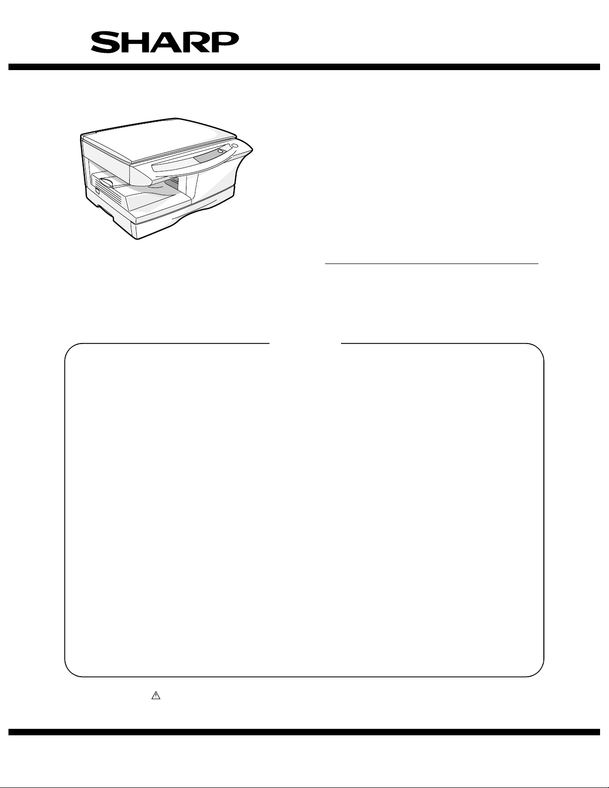
AR-5012
SERVICE MANUAL
CODE : 00ZAR5012/A1E
DIGITAL LASER COPIER/
PRINTER
MODEL
CONTENTS
[ 1 ] GENERAL . . . . . . . . . . . . . . . . . . . . . . . . . . . . . . . . . . . . . . . . . . . 1 - 1
[ 2 ] SPECIFICATIONS. . . . . . . . . . . . . . . . . . . . . . . . . . . . . . . . . . . . . 2 - 1
[ 3 ] CONSUMABLE PARTS. . . . . . . . . . . . . . . . . . . . . . . . . . . . . . . . . 3 - 1
[ 4 ] EXTERNAL VIEWS AND INTERNAL STRUCTURES . . . . . . . . . 4 - 1
[ 5 ] UNPACKING AND INSTALLATION . . . . . . . . . . . . . . . . . . . . . . . 5 - 1
[ 6 ] COPY PROCESS . . . . . . . . . . . . . . . . . . . . . . . . . . . . . . . . . . . . . 6 - 1
[ 7 ] OPERATIONAL DESCRIPTIONS . . . . . . . . . . . . . . . . . . . . . . . . . 7 - 1
[ 8 ] DISASSEMBLY AND ASSEMBLY . . . . . . . . . . . . . . . . . . . . . . . . 8 - 1
[ 9 ] ADJUSTMENTS . . . . . . . . . . . . . . . . . . . . . . . . . . . . . . . . . . . . . . 9 - 1
AR-5012
[10] SIMULATION, TROUBLE CODES . . . . . . . . . . . . . . . . . . . . . . . 10 - 1
[11] MAINTENANCE. . . . . . . . . . . . . . . . . . . . . . . . . . . . . . . . . . . . . . 11 - 1
[12] USER PROGRAMS. . . . . . . . . . . . . . . . . . . . . . . . . . . . . . . . . . . 12 - 1
[13] ELECTRICAL SECTION . . . . . . . . . . . . . . . . . . . . . . . . . . . . . . . 13 - 1
[14] CIRCUIT DIAGRAM . . . . . . . . . . . . . . . . . . . . . . . . . . . . . . . . . . 14 - 1
Parts marked with “ ” are important for maintaining the safety of the machine. Be sure to replace these parts
with the replacement parts specified to maintain the safety and performance of the machine.
This document has been published to be used
SHARP CORPORATION
for after sales service only.
The contents are subject to change without notice.
Page 2

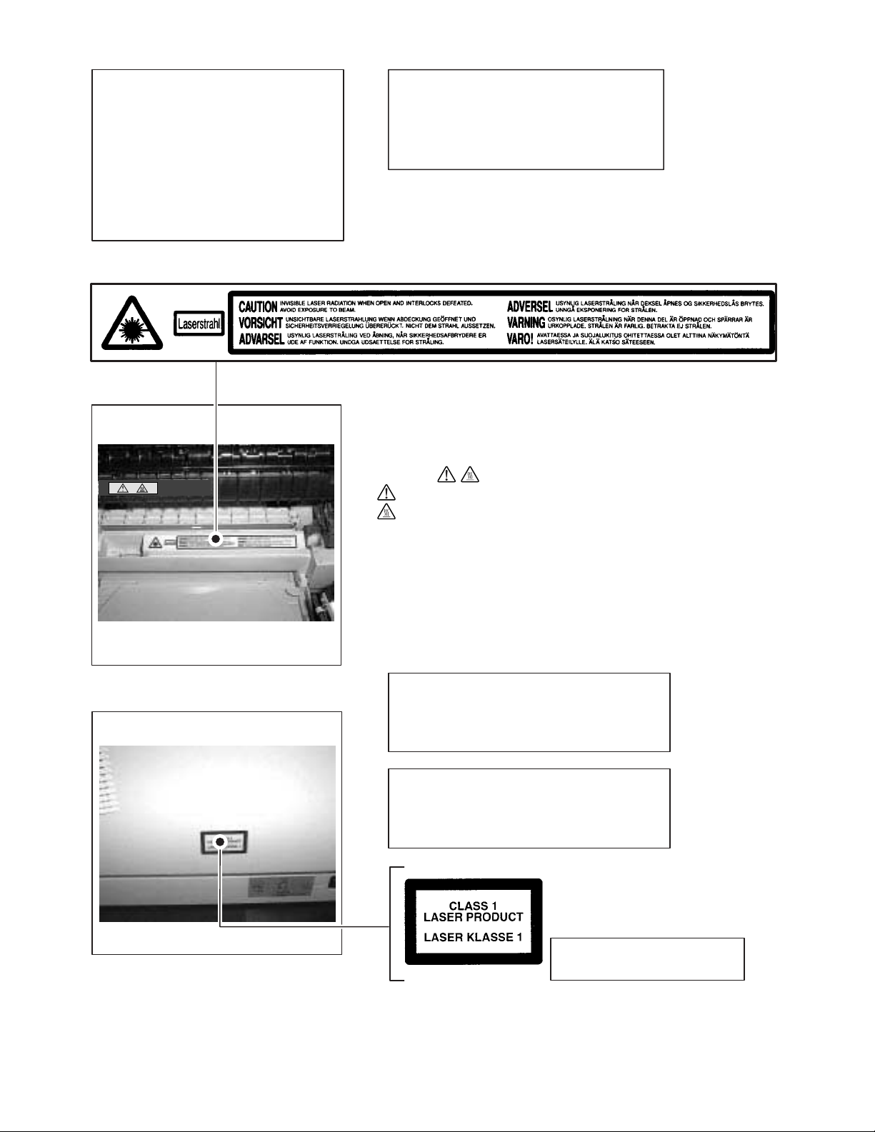
CAUTION
This product is a class 1 laser product that complies with 21CFR 1040 of the CDRH standard and
IEC825. This means that this machine does not produce hazardous laser radiation. The use of controls,
adjustments or performance of procedures other than those specified herein may result in hazardous
radiation exposure.
This laser radiation is not a danger to the skin, but when an exact focusing of the laser beam is achieved
on the eye’s retina, there is the danger of spot damage to the retina.
The following cautions must be observed to avoid exposure of the laser beam to your eyes at the time of
servicing.
1) When a problem in the laser optical unit has occurred, the whole optical unit must be exchanged as a
unit, not as individual parts.
2) Do not look into the machine with the main switch turned on after removing the developer unit, toner
cartridge, and drum cartridge.
3) Do not look into the laser beam exposure slit of the laser optical unit with the connector connected
when removing and installing the optical system.
4) The middle frame contains the safety interlock switch.
Do not defeat the safety interlock by inserting wedges or other items into the switch slot.
LASER WAVE – LENGTH : 770 ~ 795nm
Pulse times : 11.82µs/7mm
Out put power : 0.17mW
± 0.01mW
CAUTION
INVISIBLE LASER RADIATION,
WHEN OPEN AND INTERLOCKS DEFEATED.
AVOID EXPOSURE TO BEAM.
VORSICHT
UNSICHTBARE LASERSTRAHLUNG,
WENN ABDECKUNG GEÖFFNET UND
SICHERHEITSVERRIEGELUNG ÜBERBRÜCKT.
NICHT DEM STRAHL AUSSETZEN.
VARO !
AVATTAESSA JA SUOJALUKITUS
OHITETTAESSA OLET ALTTIINA
NÄKYMÄTTÖMÄLLE LASERSÄTEILYLLE ÄLÄ
KATSO SÄTEESEEN.
ADVARSEL
USYNLIG LASERSTRÅLNING VED ÅBNING, NÅR
SIKKERHEDSBRYDERE ER UDE AF
FUNKTION. UNDGÅ UDSAETTELSE FOR
STRÅLNING.
VARNING !
OSYNLIG LASERSTRÅLNING NÄR DENNA DEL
ÄR ÖPPNAD OCH SPÄRREN ÄR URKOPPLAD.
BETRAKTA EJ STRÅLEN. – STRÅLEN ÄR
FARLIG.
Page 3
At the production line, the output power
,
of the scanner unit is adjusted to 0.57
MILLI-WATT PLUS 20 PCTS and is
maintained constant by the operation of
the Automatic Power Control (APC).
Even if the APC circuit fails in operation
for some reason, the maximum output
power will only be 15 MILLI-WATT 0.1
MICRO-SEC. Giving and accessible
emission level of 42 MICRO-WATT
which is still-less than the limit of
CLASS-1 laser product.
Caution
This product contains a low power laser
device. To ensure continued safety do not
remove any cover or attempt to gain access
to the inside of the product. Refer all
servicing to qualified personnel.
Caution label on the unit
The label ( ) in the fusing area of the unit indicates the following:
: Caution, risk of danger
: Caution, hot surface
The foregoing is applicable only to the 220V
model
230V model and 240V model.
VAROITUS! LAITTEEN KÄYTTÄMINEN MUULLA
KUIN TÄSSÄ KÄYTTÖOHJEESSA MAINITULLA
TAVALLA SAATTAA ALTISTAA KÄYTTÄJÄN
TURVALLISUUSLUOKAN 1 YLITTÄVÄLLE
NÄKYMÄTTÖMÄLLE LASERSÄTEILYLLE.
VARNING - OM APPARATEN ANVÄNDS PÅ ANNAT
SÄTT ÄN I DENNA BRUKSANVISNING
SPECIFICERATS, KAN ANVÄNDAREN UTSÄTTAS
FÖR OSYNLIG LASERSTRÅLNING, SOM
ÖVERSKRIDER GRÄNSEN FÖR LASERKLASS 1.
LUOKAN 1 LASERLAITE
KLASS 1 LASER APPARAT
Page 4

CONTENTS
[1] GENERAL
1. Major functions . . . . . . . . . . . . . . . . . . . . . . . . . . . . . . . . . 1-1
[2] SPECIFICATIONS
1. Basic Specifications. . . . . . . . . . . . . . . . . . . . . . . . . . . . . . 2-1
2. Operation specifications . . . . . . . . . . . . . . . . . . . . . . . . . . 2-1
3. Copy performance. . . . . . . . . . . . . . . . . . . . . . . . . . . . . . . 2-3
[3] CONSUMABLE PARTS
1. Supply system table . . . . . . . . . . . . . . . . . . . . . . . . . . . . . 3-1
2. Environmental . . . . . . . . . . . . . . . . . . . . . . . . . . . . . . . . . . 3-1
3. Production control number (lot No.) identification . . . . . . . 3-1
4. TD cartridge replacement . . . . . . . . . . . . . . . . . . . . . . . . . 3-2
[4] EXTERNAL VIEWS AND INTERNAL STRUCTURES
1. Appearance . . . . . . . . . . . . . . . . . . . . . . . . . . . . . . . . . . . . 4-1
2. Internal. . . . . . . . . . . . . . . . . . . . . . . . . . . . . . . . . . . . . . . . 4-1
3. Operation panel. . . . . . . . . . . . . . . . . . . . . . . . . . . . . . . . . 4-2
4. Motors and solenoids . . . . . . . . . . . . . . . . . . . . . . . . . . . . 4-3
5. Sensors and switches . . . . . . . . . . . . . . . . . . . . . . . . . . . . 4-4
6. PWB unit . . . . . . . . . . . . . . . . . . . . . . . . . . . . . . . . . . . . . . 4-5
7. Cross sectional view . . . . . . . . . . . . . . . . . . . . . . . . . . . . . 4-6
[5] UNPACKING AND INSTALLATION
1. Copier installation . . . . . . . . . . . . . . . . . . . . . . . . . . . . . . . 5-1
2. Cautions on handling. . . . . . . . . . . . . . . . . . . . . . . . . . . . . 5-1
3. Checking packed components and accessories . . . . . . . . 5-1
4. Unpacking . . . . . . . . . . . . . . . . . . . . . . . . . . . . . . . . . . . . . 5-2
5. Removing protective packing materials . . . . . . . . . . . . . . . 5-2
6. Developer unit installation . . . . . . . . . . . . . . . . . . . . . . . . . 5-2
7. Toner cartridge installation . . . . . . . . . . . . . . . . . . . . . . . . 5-3
8. Loading copy paper . . . . . . . . . . . . . . . . . . . . . . . . . . . . . . 5-4
9. Power to copier . . . . . . . . . . . . . . . . . . . . . . . . . . . . . . . . . 5-4
10. Moving. . . . . . . . . . . . . . . . . . . . . . . . . . . . . . . . . . . . . . . . 5-4
[6] COPY PROCESS
1. Functional diagram . . . . . . . . . . . . . . . . . . . . . . . . . . . . . . 6-1
2. Outline of print process . . . . . . . . . . . . . . . . . . . . . . . . . . . 6-2
3. Actual print process. . . . . . . . . . . . . . . . . . . . . . . . . . . . . . 6-2
[7] OPERATIONAL DESCRIPTIONS
1. Outline of operation . . . . . . . . . . . . . . . . . . . . . . . . . . . . . . 7-1
2. Scanner section. . . . . . . . . . . . . . . . . . . . . . . . . . . . . . . . . 7-2
3. Laser unit. . . . . . . . . . . . . . . . . . . . . . . . . . . . . . . . . . . . . . 7-3
4. Fuser section. . . . . . . . . . . . . . . . . . . . . . . . . . . . . . . . . . . 7-3
5. Paper feed section and paper transport section . . . . . . . . 7-4
[8] DISASSEMBLY AND ASSEMBLY
1. High voltage section . . . . . . . . . . . . . . . . . . . . . . . . . . . . . .8-1
2. Operation panel section . . . . . . . . . . . . . . . . . . . . . . . . . . .8-4
3. Optical section. . . . . . . . . . . . . . . . . . . . . . . . . . . . . . . . . . .8-5
4. Fusing section. . . . . . . . . . . . . . . . . . . . . . . . . . . . . . . . . . .8-7
5. Tray paper feed/transport section . . . . . . . . . . . . . . . . . . . .8-9
6. Manual paper feed section . . . . . . . . . . . . . . . . . . . . . . . .8-14
7. Rear frame section . . . . . . . . . . . . . . . . . . . . . . . . . . . . . .8-16
8. Power section . . . . . . . . . . . . . . . . . . . . . . . . . . . . . . . . . .8-17
[9] ADJUSTMENTS
1. Optical section. . . . . . . . . . . . . . . . . . . . . . . . . . . . . . . . . . .9-1
2. Copy density adjustment. . . . . . . . . . . . . . . . . . . . . . . . . . .9-4
3. High voltage adjustment . . . . . . . . . . . . . . . . . . . . . . . . . . .9-5
4. Duplex adjustment . . . . . . . . . . . . . . . . . . . . . . . . . . . . . . .9-6
[10] SIMULATION, TROUBLE CODES
1. Entering the simulation mode . . . . . . . . . . . . . . . . . . . . . .10-1
2. List of simulations . . . . . . . . . . . . . . . . . . . . . . . . . . . . . . .10-2
3. Contents of simulations. . . . . . . . . . . . . . . . . . . . . . . . . . .10-3
4. Trouble codes . . . . . . . . . . . . . . . . . . . . . . . . . . . . . . . . .10-15
[11] MAINTENANCE
1. Maintenance table . . . . . . . . . . . . . . . . . . . . . . . . . . . . . . .11-1
2. Maintenance display system . . . . . . . . . . . . . . . . . . . . . . .11-1
3. Remaining toner indication . . . . . . . . . . . . . . . . . . . . . . . .11-1
4. Additional simulation and trouble code . . . . . . . . . . . . . . .11-2
[12] USER PROGRAMS
1. Functions that can be set with user programs. . . . . . . . . .12-1
2. Change the setting . . . . . . . . . . . . . . . . . . . . . . . . . . . . . .12-1
3. Density level adjustment . . . . . . . . . . . . . . . . . . . . . . . . . .12-2
4. Toner save mode setup and cancel . . . . . . . . . . . . . . . . .12-2
[13] ELECTRICAL SECTION
1. Block diagram . . . . . . . . . . . . . . . . . . . . . . . . . . . . . . . . . .13-1
2. Circuit descriptions . . . . . . . . . . . . . . . . . . . . . . . . . . . . . .13-3
[14] CIRCUIT DIAGRAM
1. MCU PWB. . . . . . . . . . . . . . . . . . . . . . . . . . . . . . . . . . . . .14-1
2. OPERATION PWB . . . . . . . . . . . . . . . . . . . . . . . . . . . . .14-10
3. POWER SUPPLY . . . . . . . . . . . . . . . . . . . . . . . . . . . . . .14-11
4. NOISE FILTER CIRCUIT . . . . . . . . . . . . . . . . . . . . . . . .14-13
5. ACTUAL WIRING DIAGRAM . . . . . . . . . . . . . . . . . . . . .14-15
Page 5
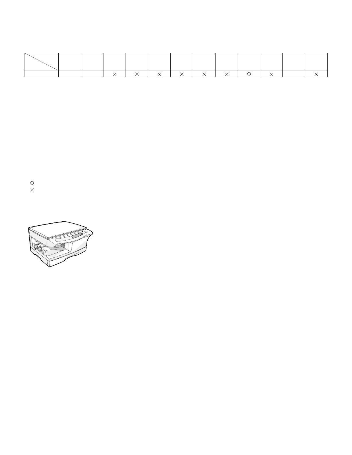
[1] GENERAL
1. Major functions
Configurations
Item
CPM SB/MB 2 Tray SPF R-SPF
Model
AR-5012 12CPM SB 8M
Descriptions of items
CPM: Copy speed (Copies Per Minute)
SB/MB: SB = Manual feed single bypass, MB = Manual feed multi bypass
2 tray: Second cassette unit.
SPF: Original feed unit
R-SPF: Duplex original feed unit
Color scanner: Color scanner function
GDI printer: GDI printer function with USB.
PCL printer: PCL printer function with USB.
SOPM: Scan Once Print Many function (Many copies are made by one scan.)
Duplex: Auto duplex copy function
Memory: Standard page memory
FAX: FAX function.
Descriptions of table
: Standard provision
: No function or no option available
Opt: Option
∗1: AL-12PKM
∗2: AR-PG2
Color
Scanner
GDI
printer
PCL
printer
SOPM Duplex Memory FAX
AR-5012
AR-5012 GENERAL 1 - 1
Page 6

[2] SPECIFICATIONS
1. Basic Specifications
Item
Type Desktop
Copy system Dry, electrostatic
Segment (class) Digital personal copier
Copier dimensions AR-5012 20.4"(W)X18.2"(D)X11.6"(H) (518mm(W)X462.5mm(D)X295.6mm(H))
Weight
(Approximately)
2. Operation specifications
Paper feed
section
Paper exit section Exit way Face down
Originals Original set Center Registration (left edge)
Optical section Scanning
Paper feed
system
AB system Tray paper feed
Inch system Tray paper feed
section
Writing
section
AR-5012 35.3lbs.(17Kg) TD and drum cartridges included
Section, item Details
AR-5012 1 tray (250 sheet) + single bypass
section
Multi bypass paper
feed section
Single bypass paper
feed section
section
Multi bypass paper
feed section
Single bypass paper
feed section
Capacity of output tray 100 sheets
Max. original size A4 (8-1/2" x 14")
Original kinds sheet, book
Original size detection None
Scanning system 3 CCDs (RGB) sensor scanning by lighting white lamp
CCD sensor Resolution 600 dpi
Lighting lamp Type CCFL
Output data R, G, B 1 or 8 bits/pixel / A/D 16bit
Writing system Writing to OPC drum by the semiconductor laser
Laser unit Resolution 600 dpi
Paper size A4, B5, A5 (Landscape)
Paper weight 56 - 80g/m
Paper feed capacity 250 sheets
Kinds Standard paper, specified paper, recycled paper
Remark User adjustment of paper guide available
Paper size A4, B5, A5, B6, A6 (Landscape)
Paper weight 52 - 128g/m
Paper feed capacity 50 sheets
Kinds Standard paper, specified paper, recycled paper, OHP,
Label, Envelop (Single copy)
Remark User adjustment of paper guide available
Paper size A4, B5, A5, B6, A6 (Landscape)
Paper weight 52 - 128g/m
Paper feed capacity 1 sheet
Kinds Standard paper, specified paper, recycled paper, OHP,
Label, Postal card, Envelop, Post card (Including
double postal without fold line)
Remark User adjustment of paper guide available
Paper size 8-1/2" x 14", 8-1/2 x 11", 8-1/2" x 5-1/2" (Landscape)
Paper weight 15 - 21 lbs.
Paper feed capacity 250 sheets
Kinds Standard paper, specified paper, recycled paper
Remark User adjustment of paper guide available
Paper size 8-1/2" x 14", 8-1/2 x 11", 8-1/2" x 5-1/2", 3-1/2" x 5-1/2"
(Landscape)
Paper weight 14 - 34.5 lbs.
Paper feed capacity 50 sheets
Kinds Standard paper, specified paper, recycled paper, OHP,
Label, Envelop (Single copy)
Remark User adjustment of paper guide available
Paper size 8-1/2" x 14", 8-1/2 x 11", 8-1/2" x 5-1/2" (Landscape)
Paper weight 14 - 34.5 lbs.
Paper feed capacity 1 sheet
Kinds Standard paper, specified paper, recycled paper, OHP,
Label, Envelop
Remark User adjustment of paper guide available
Voltage 1100Vrms (Min)
Power consumption 9.6W (Max)
2
(15 - 21 lbs.)
2
(14 - 34.5 lbs.)
2
(14 - 34.5 lbs.)
AR-5012 SPECIFICATIONS 2 - 1
Page 7

Section, item Details
Image forming Photoconductor type OPC (30ø)
Life 25k
Charger Charging system Saw -tooth charging with a grid, / (-) scorotron
discharge
Transfer system (+) DC scorotron system
Separation system (-) DC scorotron system
Developing Developing system Dry, 2-component magnetic brush development system
Cleaning Cleaning system Counter blade system (Counter to rotation)
Fusing section Fusing system Heat roller system
Upper heat roller type Teflon roller
Lower heat roller type Silicon rubber roller
Heater lamp type Halogen lamp
Voltage 120V/230V
Power consumption 800W
Electrical section Power source Voltage 100V, 110V, 120/127V, 230V, 240V
Frequency Common use for 50 and 60Hz
Power consumption Max. Less than 1000W
Average
AR-5012 300 Wh/H *1)
(during copying)
Average (stand-by) 80Wh/H *1)
Pre-heat mode 18Wh/H *1)
Auto power shut-off mode 4.5Wh/H *1)
*1) May fluctuate due to environmental conditions and the input voltage.
AR-5012 SPECIFICATIONS 2 - 2
Page 8
3. Copy performance
Section, item Details AR-5012
Copy magnification Fixed
Manual steps
(manual, photo)
Copy speed First copy time Tray paper feed 9.6 sec. (Pre-heat mode:25 sec. / Auto power-shut-off mode : 40 sec.)
AB system
A4
(Landscape)
AB system
B5
(Landscape)
Inch system
8-1/2" x 14"
(Landscape)
Inch system
8-1/2" x 11"
(Landscape)
Max. continuous copy quantity 99
Void Void area leading edge 1 - 4mm
Warm-up time 0 sec.
Power save mode reset time 0 sec.
Paper jam recovery time 0 sec.
magnification
ratios
Zooming
magnification
ratios
Copy speed
(CPM)
Copy speed
(CPM)
Copy speed
(CPM)
Copy speed
(CPM)
Image loss leading edge same size: 3.0mm or less (OC) / 4mm or less (SPF/R-SPF/Duplex)
Same size 12
Enlargement 12
Reduction 12
Same size 12
Enlargement 12
Reduction 12
Same size 12
Enlargement 12
Reduction 12
Same size 12
Enlargement 12
Reduction 12
Trailing edge 4mm or less, 6mm or less (Duplex copying/both image)
Side edge void area 0.5mm or more (per side)
3 Reduction + 2 Enlargement
(AB system : 25, 70, 86, 100, 141, 400%)
(Inch system : 25, 64, 78, 100, 129, 400%)
25 - 400%
(376 steps in 1% increments)
5 steps
A4 or Letter/100%/Auto Exposure
4.5mm or less (total of both sides)
Enlarge: 2mm or less (OC) / 3mm or less (SPF/R-SPF/Duplex)
Reduction (50%): 6.0mm or less (OC) / 8mm or less (SPF/R-SPF/
Duplex)
AR-5012 SPECIFICATIONS 2 - 3
Page 9
[3] CONSUMABLE PARTS
1. Supply system table
No. Name Content Life Product name Package Remark
1 Toner CA(Black) Toner
(Toner: Net Weight 210g)
Polyethylene bag × 10
2 Developer Developer
(Developer: Net Weight 170g)
3 Drum kit Drum × 1 25K AR-152DM 10
Drum fixing plate × 1
Note: Printing of the master/individual cartons is made in 4 languages, English/French/German/Spanish.
Packed together with the machine: DR 25K/Developer UN/Process UN
× 10 80K AR-152LT 1 LT=T ∗10
× 10 250K AR-152LD 1 LD=DV ∗10
2. Environmental
The environmental conditions for assuring the copy quality and the
machine operations are as follows:
(1) Normal operating condition
Temperature: 20°C to 25
Humidity: 65 ± 5%RH
(2) Acceptable operating condition
Humidity (RH)
85%
60%
20%
10˚C 30˚C 35˚C
(3) Optical condition
Humidity (RH)
90%
60%
15%
–25˚C30˚C40˚C
(4) Supply storage condition
Humidity (RH)
90%
20%
3. Production control number (lot No.)
identification
<Toner cartridge>
Production month
Production day
Destination code
(Dealer, distributor, OEM, etc.)
Production place
(SOCC: Fixed to B.)
End digit of year
Version No.
∗: Destination
Division No.
EX Destination
Option Destination
<Drum cartridge>
The label on the drum cartridge shows the date of production.
(SOCC production)
<JAPAN production>
X000119Ver.A 1
A same pack G
B same pack H
AP
BQ
Production month
Production day
Destination code
(Dealer, distributor, OEM, etc.)
Production place
(SOCC: Fixed to B.)
End digit of year
Version No.
Production month
(1 - 9 = Jan. - Sep. 0 = Oct. X = Nov. Y = Dec.)
Serial number of month
Fixed to 1.
Pack division
(See table below)
End digit of year
Version No.
–5˚C45˚C
AR-5012 CONSUMABLE PARTS 3 - 1
Page 10
Division No.
Ex production 1
Option 2
Same pack 3
Production control
label attachment position
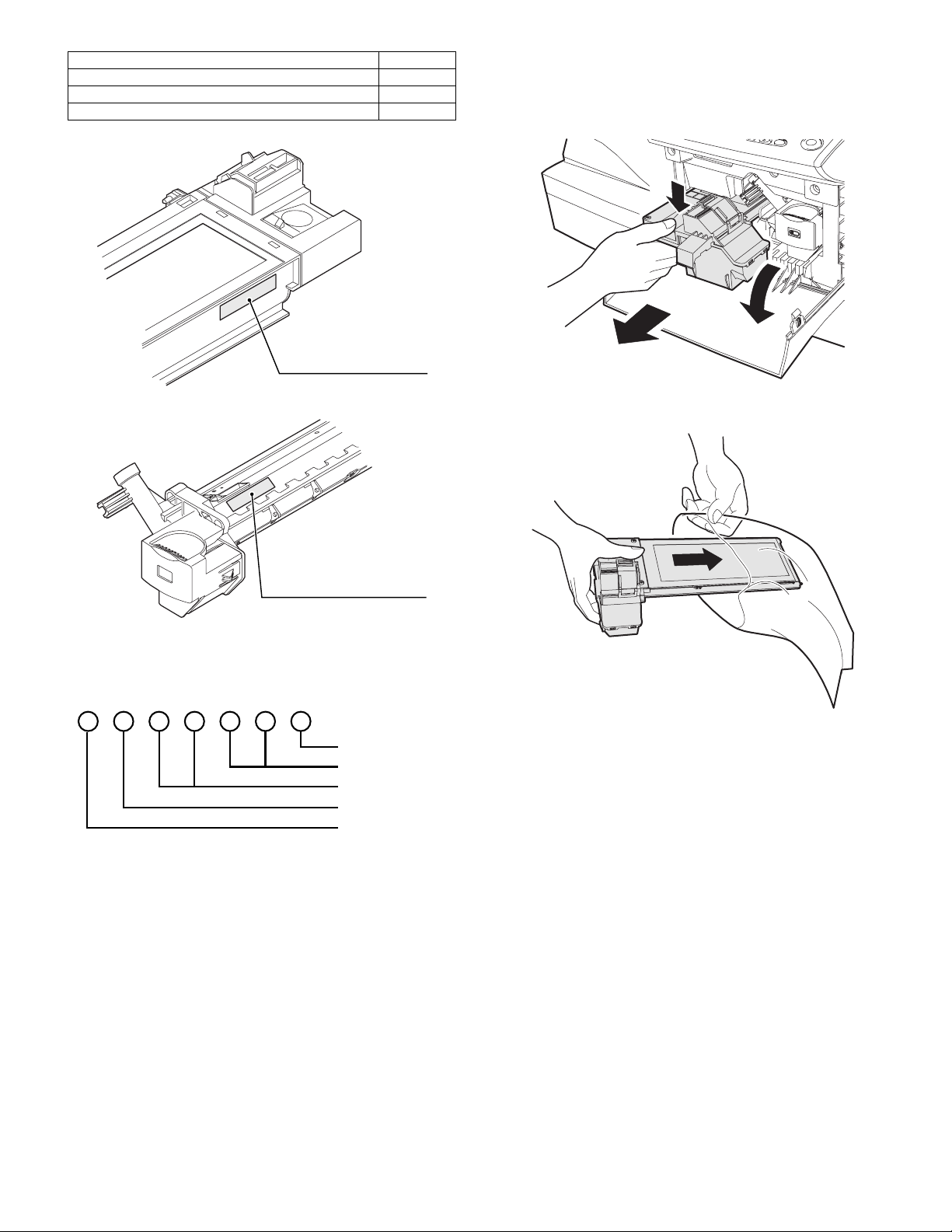
4. TD cartridge replacement
1) Open the front and side cabinets of the copier.
2) Keep holding Toner lover, and
3) Carefully pull out Toner unit from the copier.
2
3
1
4) Put Toner unit in a collection bag immediately after removing it
from the copier
Production control
label attachment position(*1)
∗1 The production control label is not attached to the cartridge of a
China product.
<Developer>
Sub lot
Production day
Production month
End digit of year
Production place
Note: Never carry exposed Toner unit. Be sure to put it in the
collection bag.
AR-5012 CONSUMABLE PARTS 3 - 2
Page 11
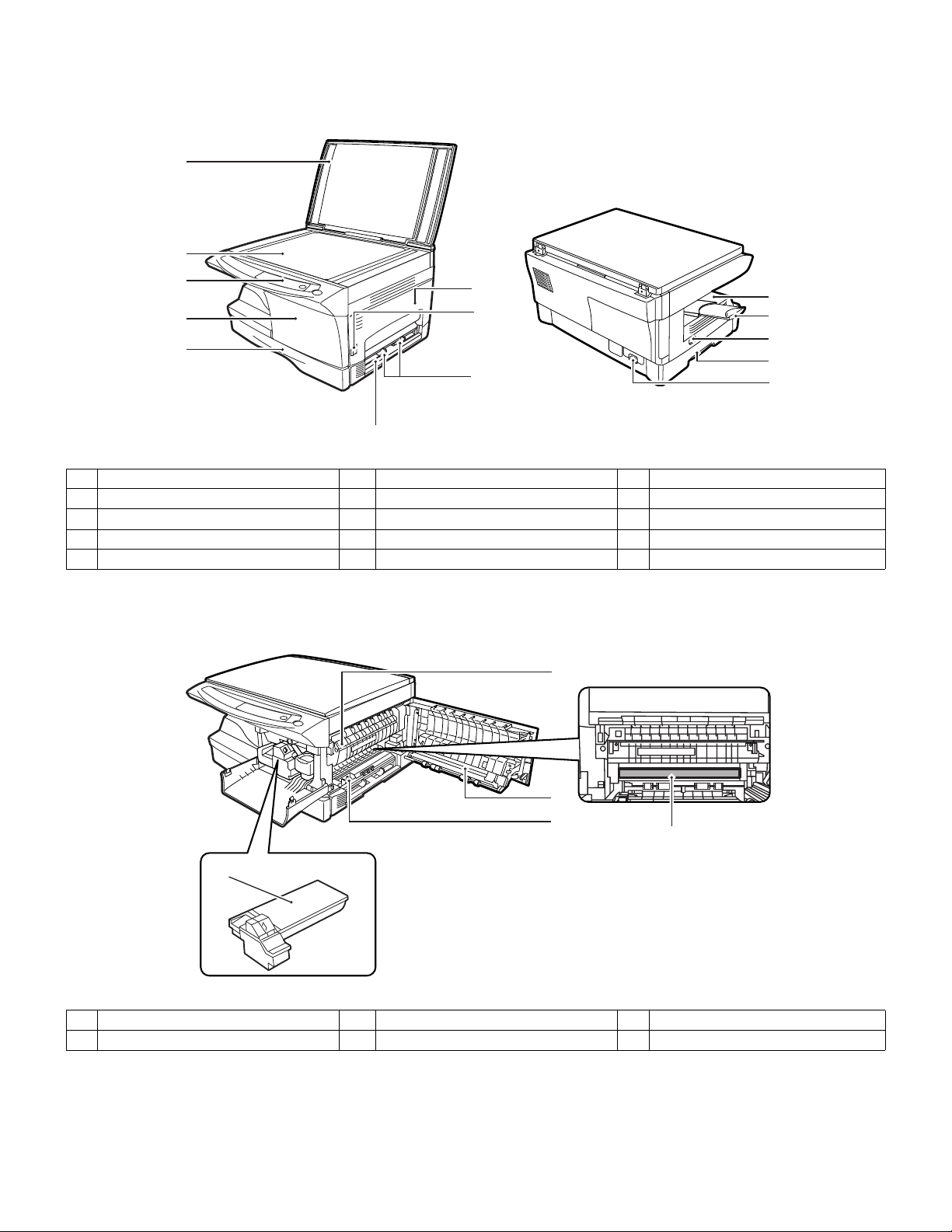
[4] EXTERNAL VIEWS AND INTERNAL STRUCTURES
1. Appearance
1
2
3
4
5
9
1 Original cover 2 Original table 3 Operation panel
4 Front cover 5 Paper tray 6 Side cover
7 Side cover open button 8 Bypass paper guides 9 Single bypass
Paper output tray 11 Paper output tray extension 12 Power switch
10
13 Handle 14 Power cord socket ——
6
7
8
10
11
12
13
14
2. Internal
2
3
4
1
1 Toner cartridge 2
4 Charger cleaner 5 Photoconductive drum ——
AR-5012 EXTERNAL VIEWS AND INTERNAL STRUCTURES 4 - 1
Fusing unit release lever
5
3 Transfer charger
Page 12
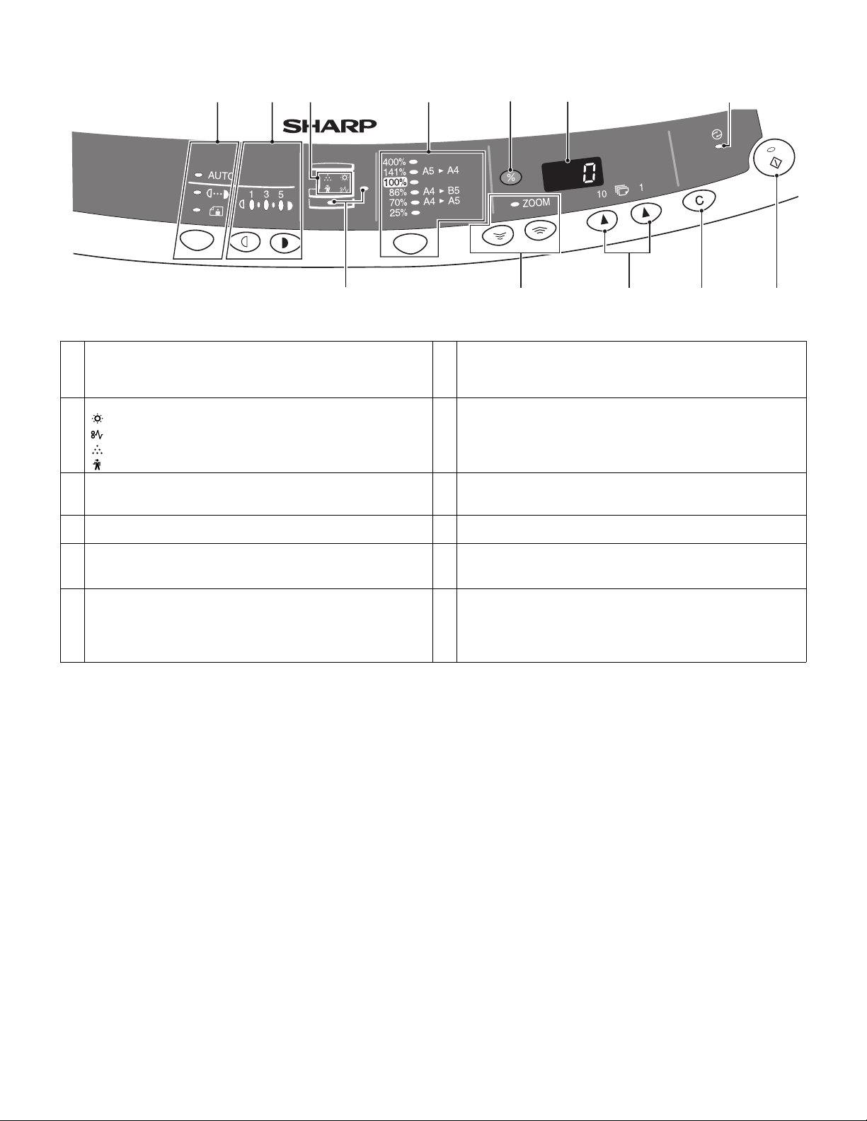
3. Operation panel
123 4 5 6
(AR-5012)
1 Exposure mode selector key and indicators
Use to sequentially select the exposure modes: AUTO, MANUAL or
PHOTO. Selected mode is shown by a lit indicator.
3 Alarm indicators
Developer replacement required indicator
Misfeed indicator
Toner cartridge replacement required indicator *1
Maintenance indicator
5 Copy ratio display (%) key 6 Display
7 Power save indicator
Lights up when the copier is in a power save mode.
9 Zoom keys / indicator
Use to select any reduction or enlargement copy ratio from 25% to
400% in 1% increments.
11 Clear key
• Press to clear the display, or press during a copy run to terminate
copying.
• Press and hold down during standby to display the total number of
copies made to date.
2 Light and dark keys and exposure indicators
Use to adjust the MANUAL or PHOTO exposure level.
Selected exposure level is shown by a lit indicator.
Use to start and terminate user program setting.
4 Copy ratio selector key and copy ratio indicators
Use to sequentially select preset reduction/enlargement copy ratios.
Selected copy ratio is shown by a lit indicator.
Displays the specified copy quantity, zoom copy ratio, user program
code, and error code.
8 Paper feed location indicators
Light up to show the selected paper feed station.
10 Copy quantity keys
• Use to select the desired copy quantity (1 to 99).
• Use to make user program entries.
12 Print key and ready indicator
• Copying is possible when the indicator is on.
• Use to set a user program.
• Press to start copying
7
12111098
AR-5012 EXTERNAL VIEWS AND INTERNAL STRUCTURES 4 - 2
Page 13
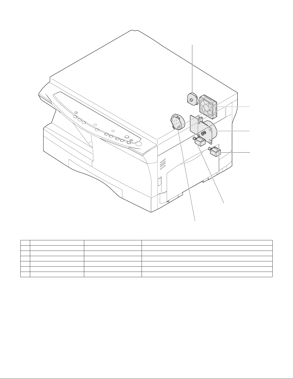
4. Motors and solenoids
2
4
1
5
3
No. Part name Control signal Function / Operation
1 Main motor MM Drives the copier.
2 Scanner motor MRMT Drives the optical mirror base (scanner unit).
3 Toner motor TM Supplies toner.
4 Cooling fan motor VFM Cools the optical section.
5 Resist roller solenoid RRS Resist roller rotation control solenoid
6 Paper feed solenoid CPFS1 Cassette Paper feed solenoid 1
6
AR-5012 EXTERNAL VIEWS AND INTERNAL STRUCTURES 4 - 3
Page 14
5. Sensors and switches
1
2
3
5
6
7
No. Name Signal Type Function Output
1 Scanner unit home position
sensor
2 POD sensor POD Transmission sensor Paper exit detection "H" at paper pass
3 PPD2 sensor PPD2 Transmission sensor Paper transport detection 2 "L" at paper pass
4 Cassette detection switch CED1 Micro-switch Cassette installation detection "L" at cassette insertion
5 Manual feed detection
switch
6 PPD1 sensor PPD1 Transmission sensor Paper transport detection 1 "L" at paper pass
7 Door switch DSW Micro-switch Door open/close detection
MHPS Transmission sensor Scanner unit home position detection "H" at home position
MFD Transmission sensor Manual feed paper detection
(single only)
(safety switch for 24V)
"L" at paper detection
1 or 0V of 24V at door open
4
AR-5012 EXTERNAL VIEWS AND INTERNAL STRUCTURES 4 - 4
Page 15
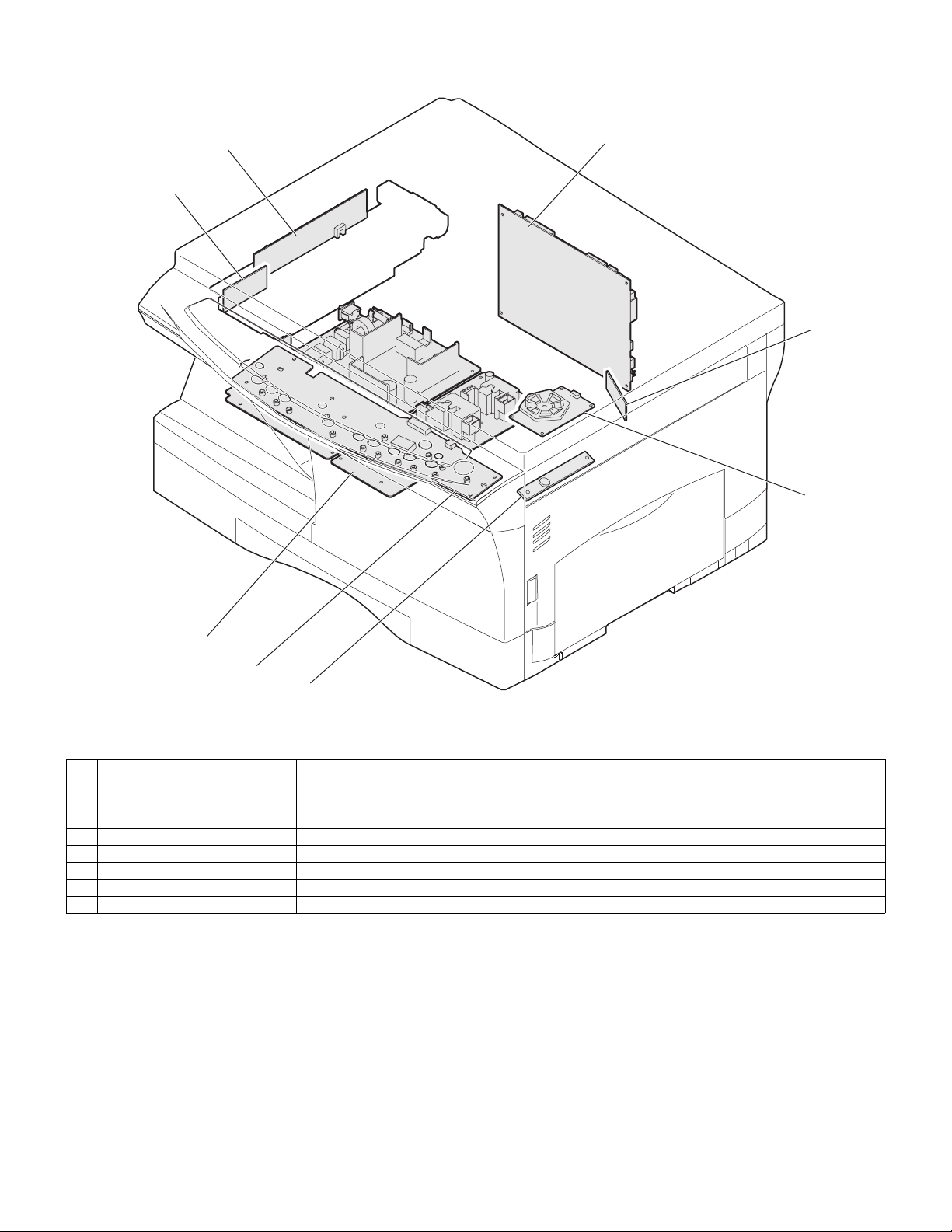
6. PWB unit
5
2
1
8
6
4
3
7
No. Name Function
1 Exposure lamp invertor PWB Exposure lamp (CCFL) control
2 Main PWB (MCU) Copier control
3 Operation PWB Operation input/display
4 Power PWB AC power input, DC voltage control, High voltage control
5 CCD sensor PWB For image scanning
6 LSU motor PWB For polygon motor drive
7 TCS PWB For toner sensor control
8 LSU PWB For laser control
AR-5012 EXTERNAL VIEWS AND INTERNAL STRUCTURES 4 - 5
Page 16
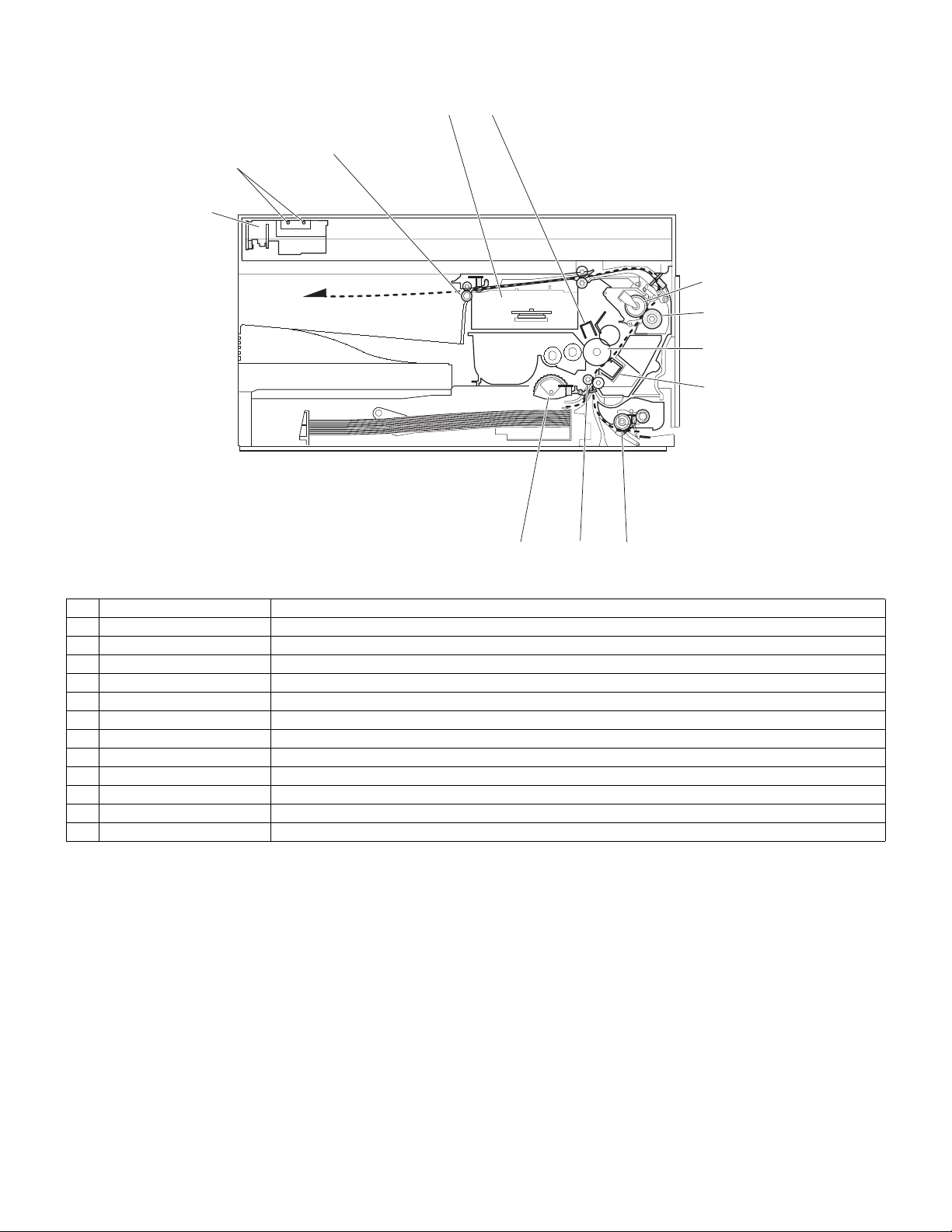
7. Cross sectional view
3
5
2
4
1
6
7
8
9
12
11
10
No. Part name Function and operation
1 Scanner unit Illuminates the original with the copy lamp and passes the reflected light to the lens unit(CCD).
2 Exposure lamp Exposure lamp (CCFL) Illuminates original
3 LSU (Laser unit) Converts the original image signal into laser beams and writes onto the drum.
4 Paper exit roller Roller for paper exit
5 Main charger Provides negative charges evenly to the drum surface.
6 Heat roller Fuses toner on the paper. (Teflon roller)
7 Pressure roller Fuses toner on the paper. (Silicon rubber roller)
8 Drum Forms images.
9 Transfer unit Transfers images onto the drum.
10 Manual paper feed roller Transport the paper from the manual paper feed port.
11 PS roller unit Takes synchronization between the lead edge and the rear edge of the paper.
12 Paper feed roller Picks up a sheet of paper from the cassette.
AR-5012 EXTERNAL VIEWS AND INTERNAL STRUCTURES 4 - 6
Page 17
[5] UNPACKING AND INSTALLATION
1. Copier installation
Improper installation may damage the copier. Please note the following
during initial installation and whenever the copier is moved.
Caution: If the copier is moved from a cool place to a warm place, con-
densation may form inside the copier. Operation in this condition will cause poor copy quality and malfunctions.
Leave the copier at room temperature for at least 2 hours
before use.
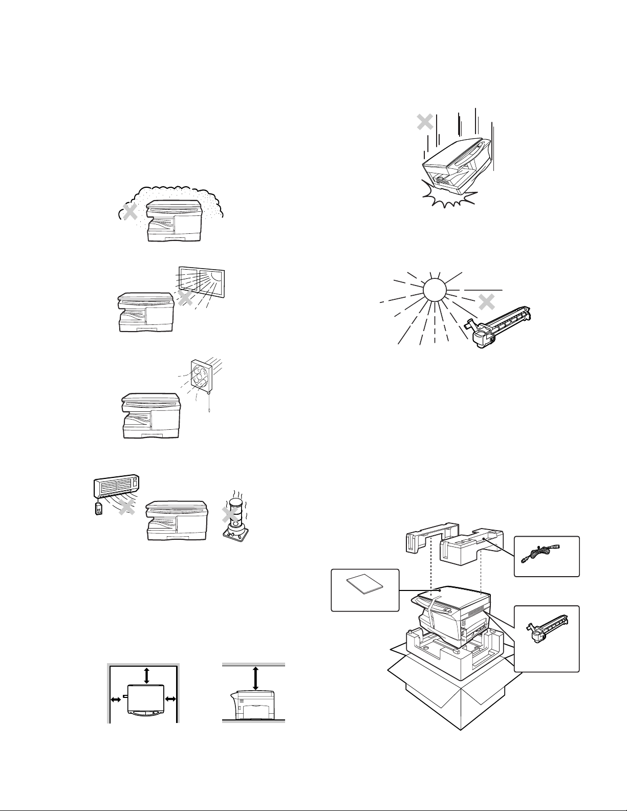
Do not install your copier in areas that are:
• damp, humid, or very dusty
• exposed to direct sunlight
2. Cautions on handling
Be careful in handling the copier as follows to maintain the performance of this copier.
Do not drop the copier, subject it to shock or strike it against any
object.
Do not expose the drum cartridge to direct sunlight.
Doing so will damage the surface (green portion) of the drum cartridge,
causing poor print quality.
• poorly ventilated
• subject to extreme temperature or humidity changes, e.g., near an
air conditioner or heater.
The copier should be installed near an accessible power outlet for easy
connection.
Be sure to connect the power cord only to a power outlet that meets
the specified voltage and current requirements.
Also make certain the outlet is properly grounded.
Be sure to allow the required space around the machine for servicing
and proper ventilation.
20cm (8")
Store spare supplies such as drum cartridges and TD cartridges in a
dark place without removing from the package before use.
If they are exposed to direct sunlight, poor print quality may result.
Do not touch the surface (green portion) of the drum cartridge.
Doing so will damage the surface of the cartridge, causing poor print
quality.
3. Checking packed components and
accessories
Open the carton and check if the following components and accessories are included.
Power cord
Operation manual
Drum cartridge
(installed in unit)
10cm
(4")
10cm
(4")
20cm (
AR-5012 UNPACKING AND INSTALLATION 5 - 1
Page 18
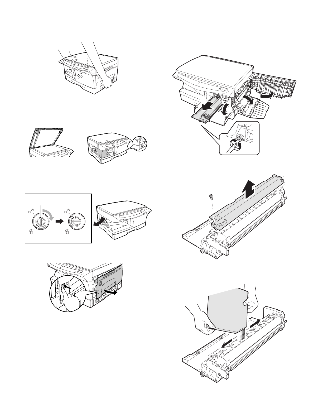
4. Unpacking
6. Developer unit installation
Be sure to hold the handles on both sides of the copier to unpack the
copier and carry it to the installation location.
5. Removing protective packing materials
1) Remove pieces of tape and protective cover. Then open the original cover and remove protective materials (a) and (b).
AR-5012AR-5012
1) 2) 3) Open the side and front cabinets of the copier.
4) Remove the locking tape of the developer unit.
5) Remove the screw which is fixing the copier and Developer unit.
6) Remove Developer unit slowly from the copier.
5
1
2
3
4
7) Remove the screw (1 pc).
8) Remove Upper developer unit.
2) Release the scan head locking switch.
Grasp here and turn in
the direction of the arrow.
Lock Unlock
3) Ensure that the bypass tray is open and then open the side cover
by pressing the open button on the side cover.
9) Shake the aluminum bag to stir developer
10) Supply developer from the aluminum bag to the top of the MX roller
evenly.
Note: Be careful not to splash developer outside Developer unit.
AR-5012 UNPACKING AND INSTALLATION 5 - 2
Page 19
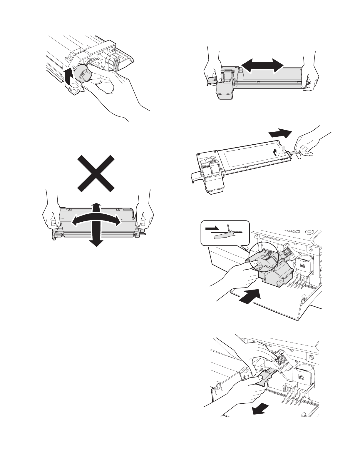
11) Attach Upper developer unit and fix it with a screw.
12) Rotate the MG roller gear to distribute developer evenly.
Note: Never rotate the gear in the reverse direction.
Note: When carrying Developer unit, do not tilt it extremely as
shown with the arrow in the figure below.
(Prevention of splash of developer)
7. Toner cartridge installation
1) To prevent against uneven distribution of toner, hold Toner unit
with both hands and shake it several times horizontally.
2) Hold the section of Toner unit shown in the figure below, remove
the packing tape, and remove the cushion.
3) Pull out the cushion in the arrow direction.
13) Insert Developer unit carefully into the copier.
Note: Quick insertion may result in splash of developer. Be sure to
insert carefully.
14) Confirm that Developer unit is completely inserted to the bottom of
the machine, fix Developer unit and the machine with a screw.
15) Completion of Developer unit installation
4) Insert Toner unit carefully into the copier.
5) Insert until the hook is engaged with the copier as shown in the figure below.
6) Pull out the shutter in the arrow direction.
Note: Do not hold and carry the shutter. Otherwise the shutter may
drop and Toner unit may drop.
7) Completion of Toner unit installation
Close the front and side cabinets.
AR-5012 UNPACKING AND INSTALLATION 5 - 3
Page 20
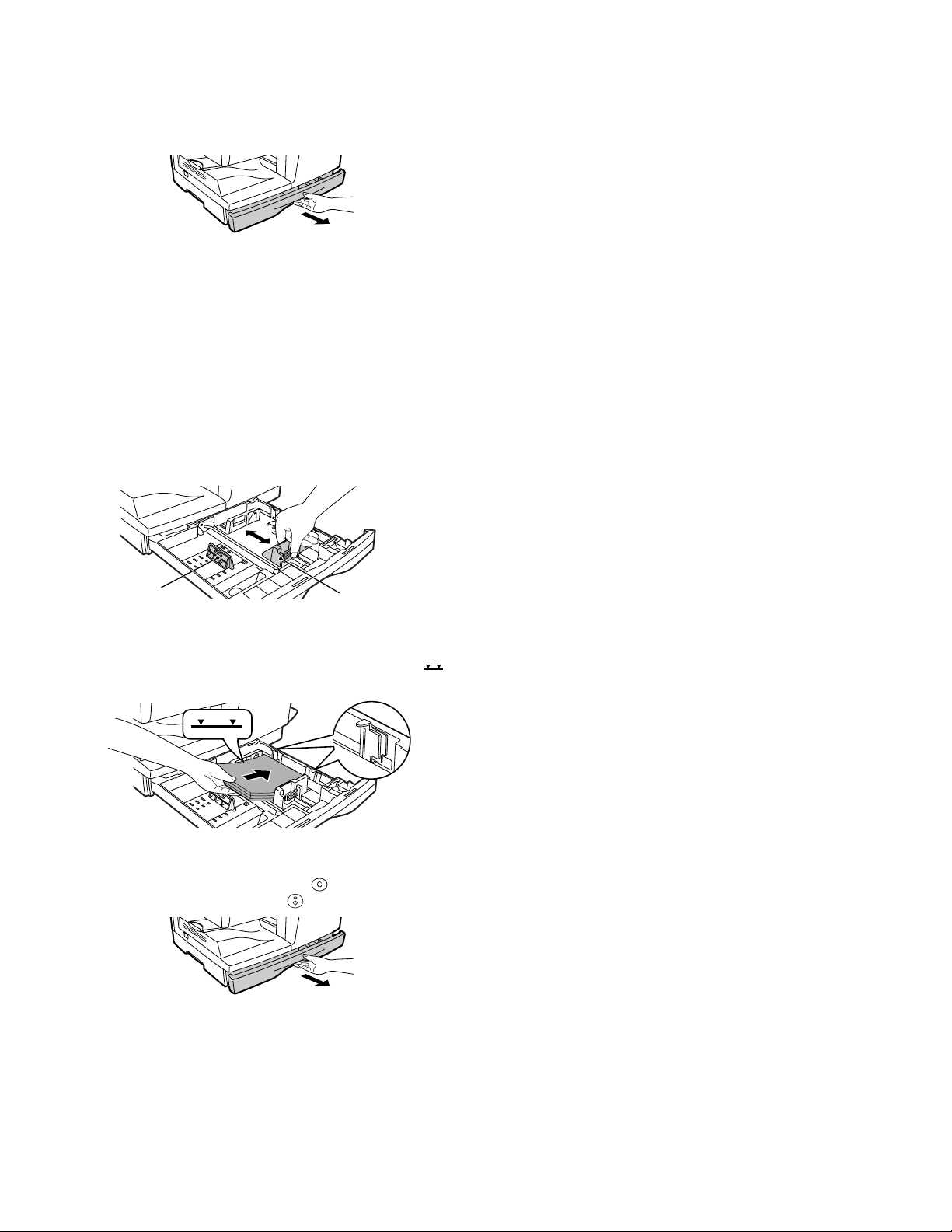
8. Loading copy paper
9. Power to copier
Note: This copier is equipped with two paper trays. Load copy paper
into the two paper trays.
1) Raise the handle of the paper tray and pull the paper tray out until
it stops.
2) Remove the pressure plate lock. Rotate the pressure plate lock in
the direction of the arrow to remove it while pressing down the
pressure plate of the paper tray.
3) Store the pressure plate lock that was removed in step 2 and the
screw that was removed when unpacking the machine in the front
of the paper tray. To store the pressure plate lock, rotate the lock
to fix it on the relevant location.
4) Adjust the paper guides on the paper tray to the copy paper width
and length.
Squeeze the lever of paper guide (A) and slide the guide to match
with the width of the paper.
Move paper guide (B) to the appropriate slot as marked on the
tray.
Paper
guide (B)
5) Fan the copy paper and insert it into the tray. Make sure the edges
go under the corner hooks.
Note: Do not load paper above the maximum height line ( ).
Exceeding the line will cause a paper misfeed.
Paper
guide (A)
1) Ensure that the power switch of the copier is in the OFF position.
Insert the attached power cord into the power cord socket at the
rear of the copier.
2) Plug the other end of the power cord into the nearest outlet.
10. Moving
Moving instructions
When moving the unit, follow the procedure below.
Note: When moving this unit, be sure to remove the TD cartridge in
advance.
1) Turn the power switch off and remove the power cord from the out-
let.
2) Open the side cover and front cover, in that order. Remove the TD
cartridge and close the front cover and side cover, in that order.
To open and close the side cover and front cover, and to remove
the TD cartridge, see "TD CARTRIDGE REPLACEMENT".
3) Raise the handle of the paper tray and pull the paper tray out until it
stops.
4) Push the center of the pressure plate down until it locks in place
and lock the plate using the pressure plate lock which has been
stored in the front of the paper tray.
5) Push the paper tray back into the unit.
6) Lock the scan head locking switch.
Note: When shipping the unit, the scan head locking switch must be
locked to prevent shipping damage.
7) Close the multi-bypass tray and the paper output tray extension,
and attach the packing materials and tape which were removed
during installation of the unit. See "PREPARING THE UNIT FOR
INSTALLATION".
8) Pack the unit into the carton. See "CHECKING PACKED COMPO-
NENTS AND ACCESSORIES".
6) Gently push the paper tray back into the copier.
Note: After loading copy paper, to cancel the blinking "H" without
restarting copying, press the clear ( ) key. The "P" in the
display will go out and the ready ( ) indicator will light up.
AR-5012 UNPACKING AND INSTALLATION 5 - 4
Page 21
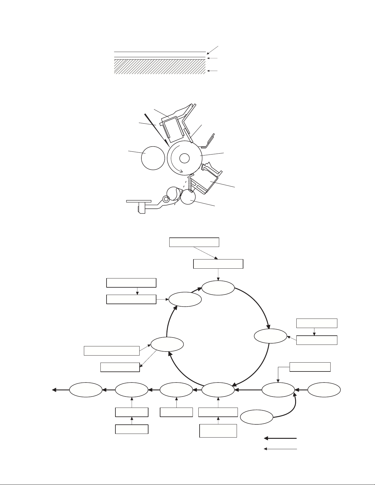
[6] COPY PROCESS
1. Functional diagram
An OPC drum is used for the photoconductor.
(Structure of the OPC drum layers)
Main charger
OPC layer
(20 microns thick)
Pigment layer (0.2
to 0.3 microns thick)
Aluminum drum
(Basic operation cycle)
Laser beam
MG roller
Main high voltage unit
Cleaning blade
Drum
Transfer unit
Resist roller
Semiconductor laser
Focus correction lens
Exposure
To face
down tray
Saw tooth
Cleaning blade
Waste toner box
Paper release Fusing
Heat roller
Heater lamp
Charge
Drum
Cleaning
Separation
Electrode
AR-5012 COPY PROCESS 6 - 1
Transfer
Transfer charger
Transfer high
voltage unit
Developing
Cassette
paper feed
Synchronization
with drum
Toner
Developer
PS roller
Manual feed
Print process
Paper transport route
Page 22
2. Outline of print process
This printer is a non-impact printer that uses a semiconductor laser
and electrostatic print process. This printer uses an OPC (Organic
Photo Conductor) for its photoconductive material.
First, voltage from the main corona unit charges the drum surface and
a latent image is formed on the drum surface using a laser beam. This
latent image forms a visible image on the drum surface when toner is
applied. The toner image is then transferred onto the print paper by the
transfer corona and fused on the print paper in the fusing section with
a combination of heat and pressure.
Step-1: Charge
Step-2: Exposure
* Latent image is formed on the drum.
Step-3: Developing
Latent image formed on the drum is then changed into visible
image with toner.
Step-4: Transfer
The visible image (toner image) on the drum is transferred
onto the print paper.
Step-5: Cleaning
Residual toner on the drum surface is removed and collected
by the cleaning blade.
Step-6: Optical discharge
Residual charge on the drum surface is removed, by
semiconductor laser beam.
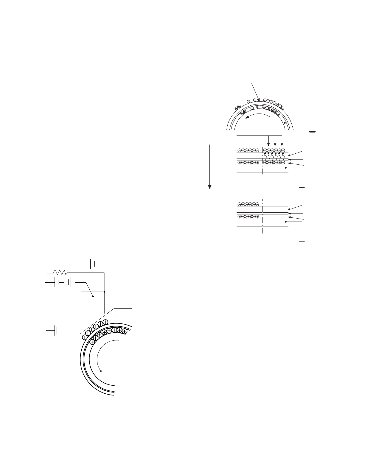
3. Actual print process
Step-1: DC charge
A uniform negative charge is applied over the OPC drum surface by
the main charging unit. Stable potential is maintained by means of the
Scorotron charger.
Positive charges are generated in the aluminum layer.
Step-2: Exposure (laser beam, lens)
A Laser beam is generated from the semiconductor laser and
controlled by the print pattern signal. The laser writes onto the OPC
drum surface through the polygon mirrors and lens. The resistance of
the OPC layer decreases for an area exposed by the laser beam
(corresponding to the print pattern signal). The beam neutralizes the
negative charge. An electrostatic latent image is formed on the drum
surface.
Semiconductor laser
Exposure
(semiconductor laser)
OPC layer
Pigment
layer
Aluminum
drum
Drum surface charge
after the exposure
OPC layer
Pigment
layer
Aluminum
Non-image area Image area
layer
About
DC5.5KV
( 580V/ 390V)
AR-5012 COPY PROCESS 6 - 2
Page 23
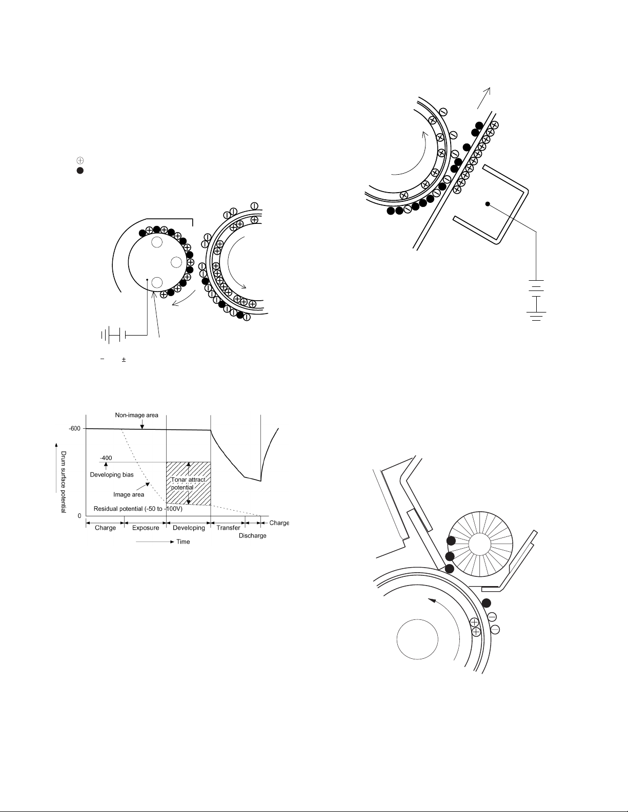
Step-3: Developing (DC bias)
A bias potential is applied to the MG roller in the two component
magnetic brush developing method, and the toner is charged negative
through friction with the carrier.
Non-image area of the drum surface charged with negative potential
repel the toner, whereas the laser exposed portions where no negative
charges exist, attract the toner. As a result, a visible image appears on
the drum surface.
:Carrier (Magnetized particle)
:Toner (Charge negative by friction)
(N) (S) Permanent magnet
(provided in three locations)
N
S
N
Step-4: Transfer
The visible image on the drum surface is transferred onto the print
paper by applying a positive charge from the transfer corona to the
backside of the print paper.
About DC 5.2kV
DC
400V 8V
Toner is attracted over the shadowed area because of the developing
bias.
MG roller
Step-5: Separation
Since the print paper is charged positively by the transfer corona, it is
discharged by the separation corona. The separation corona is
connected to ground.
Step-6: Cleaning
Toner remaining on the drum is removed and collected by the cleaning
blade. It is transported to the waste toner collecting section in the
cleaning unit by the waste toner transport roller.
AR-5012 COPY PROCESS 6 - 3
Page 24

Step-7: Optical discharge (Semiconductor laser)
Before the drum rotation is stopped, the semiconductor laser is
radiated onto the drum to reduce the electrical resistance in the OPC
layer and eliminate residual charge, providing a uniform state to the
drum surface for the next page to be printed.
When the electrical resistance is reduced, positive charges on the
aluminum layer are moved and neutralized with negative charges on
the OPC layer.
Semiconductor laser
Charge by the Scorotron charger
Function
The Scorotron charger functions to maintain uniform surface potential
on the drum at all times, It control the surface potential regardless of
the charge characteristics of the photoconductor.
Basic function
A screen grid is placed between the saw tooth and the
photoconductor. A stable voltage is added to the screen grid to
maintain the corona current on the photoconductor.
As the photoconductor is charged by the saw tooth from the main
corona unit, the surface potential increases. This increases the current
flowing through the screen grid. When the photoconductor potential
nears the grid potential, the current turns to flow to the grid so that the
photoconductor potential can be maintained at a stable level.
Start
1) Because the grid potential is at a low level, the drum potential is at
about -400V. (Carrier may not be attracted though the carrier is
pulled towards the drum by the electrostatic force of -400V.
2) Developing bias (-400V) is applied when the photoconductor
potential is switched from LOW to HIGH.
3) Once developing bias (-400V) is applied and the photo conductor
potential rises to HIGH, toner will not be attracted to the drum.
Stop
The reverse sequence takes place.
Retaining developing bias at an abnormal occurrence
Function
The developing bias will be lost if the power supply was removed
during print process. In this event, the drum potential slightly abates
and the carrier makes deposits on the drum because of strong static
power. To prevent this, the machine incorporates a function to retain
the developing bias for a certain period and decrease the voltage
gradually against possible power loss.
Basic function
Normally, the developing bias voltage is retained for a certain time
before the drum comes to a complete stop if the machine should stop
before completing the normal print cycle. The developing bias can be
added before resuming the operation after an abnormal interruption.
Therefore, carrier will not make a deposit on the drum surface.
Process controlling
Function
The print pattern signal is converted into an invisible image by the
semiconductor laser using negative to positive (reversible) developing
method. Therefore, if the developing bias is added before the drum is
charged, toner is attracted onto the drum. If the developing bias is not
added when the drum is charged, the carrier is attracted to the drum
because of the strong electrostatic force of the drum.
To avoid this, the process is controlled by adjusting the drum potential
and the grid potential of the Scorotron charger.
Basic function
Voltage added to the screen grid can be selected, high and low. To
make it easily understood, the figure below shows voltage transition at
the developer unit.
START STOP
0
Toner attract
potentia l
2)
3)
1)
Low
Print potential
Develop ing bias
4)
High
Time
Drum potential
AR-5012 COPY PROCESS 6 - 4
Page 25
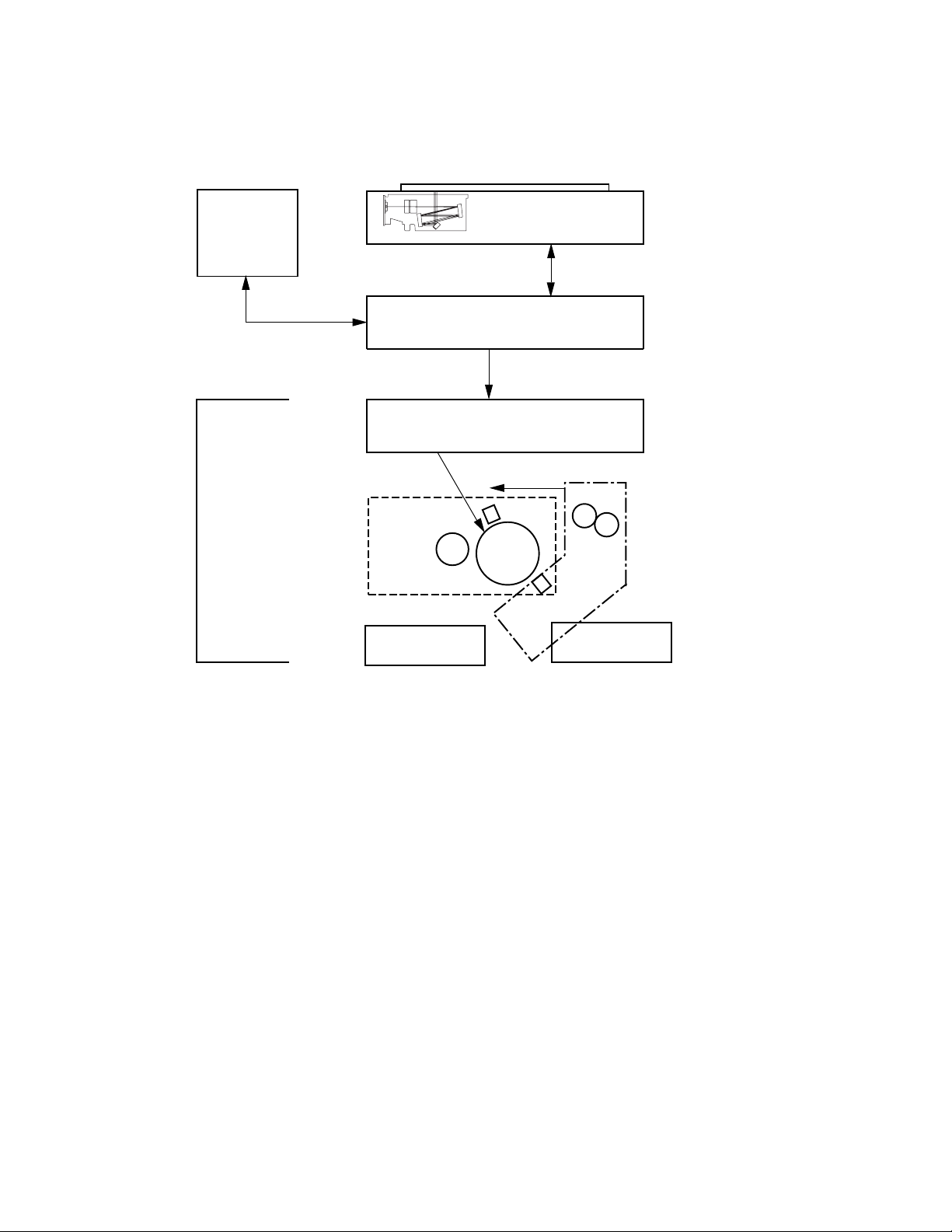
[7] OPERATIONAL DESCRIPTIONS
1. Outline of operation
The outline of operation is described referring to the basic configuration.
(Basic configuration)
Scanner section
Operation
section
Printer section
CCD
MCU (Main control/image process section)
LSU (Laser unit)
Laser diode, Polygon mirror lens
Laser beam
Process section
Cassette paper
feed section
Paper exit
Fusing section
Paper transport section
Manual paper
feed section
(Outline of copy operation)
Setting conditions
1) Set copy conditions such as the copy quantity and the copy density
with the operation section, and press the COPY button. The
information on copy conditions is sent to the MCU.
Image scanning
2) When the COPY button is pressed, the scanner section starts
scanning of images.
The light from the copy lamp is reflected by the document and
passed through the lens to the CCD.
Photo signal/Electric signal conversion
3) The image is converted into electrical signals by the CCD circuit
and passed to the MCU.
Image process
4) The document image signal sent from the CCD circuit is processed
under the revised conditions and sent to the LSU (laser unit) as
print data.
Electric signal/Photo signal (laser beam) conversion
5) The LSU emits laser beams according to the print data.
(Electrical signals are converted into photo signals.)
6) The laser beams are radiated through the polygon mirror and
various lenses to the OPC drum.
Printing
7) Electrostatic latent images are formed on the OPC drum according
to the laser beams, and the latent images are developed to be
visible images(toner images).
8) Meanwhile the paper is fed to the image transfer section in
synchronization with the image lead edge.
9) After the transfer of toner images onto the paper, the toner images
are fused to the paper by the fusing section. The copied paper is
discharged onto the exit tray.
AR-5012 OPERATIONAL DESCRIPTIONS 7 - 1
Page 26
2. Scanner section
A. Scanner unit
The scanner unit in the digital copier scans images.
It is composed of the optical unit and the drive unit. The optical unit
performs scanning in the main scan direction with the light receiving
elements (color CCD). The drive unit performs scanning in the sub
scanning direction by moving the optical unit.
B. Optical system
Two white lamps are used as the light source.
Light radiated from the light source is applied to the document on the
document table. The reflected light from the document is reflected 5
times by No. 1 - No. 3 mirrors and passed through the reduction lens to
form images on the light-receiving surface of 3-line CCD.
The light-receiving surface of the color CCD is provided with 3 line
scanning sections for RGB. Separate images scanned in each color
section are overlapped to complete color scanning. (When PC scanning)
The resolution is 600dpi.
When copying, only the green component is used to print with the
printer.
The color component for printing can be switched to red or blue by the
service simulation.
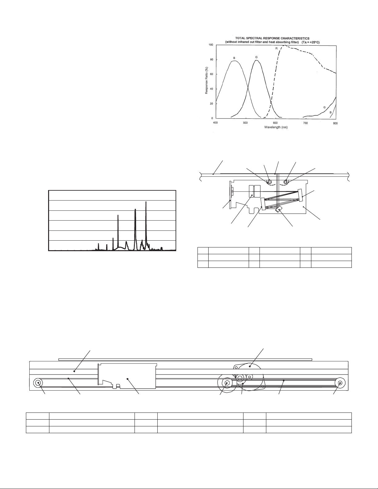
(Spectrum characteristics of the color CCD)
1
9
10
8
8
9
6.00E-01
5.00E-01
4.00E-01
3.00E-01
Intensity of UV
2.00E-01
1.00E-01
0.00E+00
Lamp : MBVM26W25W260NLH/G
Lamp current : 5mA
Temp. : 25 degree
0 200 400 600 800
MBVM26W25W260NLH/G
Wave length (nm)
(Spectrum characteristics of the lamp)
C. Drive system
The drive system is composed of the scanner motor, the pulley gear,
the idle pulley, the idle gear, the belt 473, the belt 190, and the shaft.
The motor rotation is converted into reciprocated movements of the
belt 473 through the idle gear, the pulley gear, the belt 190, and the
idle pulley to drive the optical unit.
7
6
7
3
5
4
2
(Optical unit)
1 Table glass 2 Optical unit 3 Lens
4 Mirror 1 5 Mirror 2 6 Mirror 3
7 CCD PWB 8 Lamp 9 Reflector
1
34 6 285
1 Scanner motor 2 Pulley gear 3 Idle pulley
4 Belt 473 5 Belt 190 6 Optical unit
7 Shaft 8 Idle gear 9
AR-5012 OPERATIONAL DESCRIPTIONS 7 - 2
3
Page 27
3. Laser unit
The image data sent from the MCU (image process circuit) is sent to
the LSU (laser unit), where it is converted into laser beams.
A. Basic structure
The LSU unit is the writing section of the digital optical system.
The semiconductor laser is used as the light source, and images are
formed on the OPC drum by the polygon mirror and fθ lens, etc.
The laser beams are passed through the collimator lens, the cylindrical
lens, the polygon mirror, the fθ lens, and the mirror to form images on
the OPC drum in the main scanning direction. The laser emitting PWB
is provided with the APC (auto power control) in order to eliminate fluctuations in the laser power. The BD PWB works for measurement of
the laser writing start point.
B. Laser beam path
4
1
2
No Component Function
1 Semiconductor laser Generates laser beams.
2 Collimator lens Converges laser beams in parallel.
3 Polygon mirror,
polygon motor
4 BD (Mirror, lens, PWB) Detects start timing of laser scanning.
5fθ lens Converges laser beams at a spot on the
Makes the laser scanning speeds at both ends of the drum same as
each other.
Reflects laser beams at a constant rpm.
drum.
Makes the laser scanning speeds at both
ends of the drum same as each other.
(Refer to the figure below.)
5
3
C. Composition
Effective scanning width: 216mm (max.)
Resolution: 600dpi
Beam diameter: 75um in the main scanning direction, 80um in the sub
scanning direction
Image surface power: 0.17 ±0.01mW (Laser wavelength 770 - 795nm)
Polygon motor section: Brushless motor 20.787rpm
No. of mirror surfaces: 6 surfaces
4. Fuser section
a ≠ b ≠ c
ab c
d = e = f
def
A. General description
f θ LENS
AR-5012 OPERATIONAL DESCRIPTIONS 7 - 3
General block diagram (cross section)
Thermistor
Heat roller
Thermal fuse
Separator pawl
PPD2
Pressure roller
Paper guide
Page 28
Top view
Heat roller
Thermistor
Thermal fuse
Heater lamp
5. Paper feed section and paper transport
section
A. Paper transport path and general operations
Separator pawl
(1) Heat roller
A Teflon roller is used for the heat roller and a silicone rubber roller is
used for the lower heat roller for better toner fusing performance and
paper separation.
(2) Separator pawl
Three separator pawls are used on the upper heat roller. The separator pawls are Teflon coated to reduce friction with the roller and prevent
a smear on the paper caused by the separator pawl.
(3) Thermal control
1) The heater lamp, thermistor, main PWB, DC power supply PWB,
and triac within the power supply unit are used to control the
temperature in the fuser unit.
To prevent against abnormally high temperature in the fuser unit, a
thermal breaker and thermal fuse are used for safety purposes.
Heated by the heater
lamp. (950W)
Safety device
(thermal breaker, thermal
fuse)
Triac (in the
power supply unit)
The surface temperature
of the upper heat roller is
sensed by the thermistor.
Level of the thermistor is
controlled by the main PWB.
54 3
2
1
6
7
8
9
10
11121314
1 Scanner unit 8 Drum
2 Copy lamp 9 Transfer unit
3 LSU (Laser unit) 10 Pickup roller
4 Paper exit roller 11 Manual paper feed tray
5 Main charger 12 Manual paper feed roller
6 Heat roller 13 PS roller unit
7 Pressure roller 14 Paper feed roller
Paper feed is made in two ways; the tray paper feed and the manual
paper feed. The tray is of universal-type, and has the capacity of 250
sheets.
The front loading system allows you to install or remove the tray from
the front cabinet.
The general descriptions on the tray paper feed and the manual paper
feed operation are given below.
(1) Cassette paper feed operation
1) The figure below shows the positions of the pick-up roller, the
paper feed clutch sleeve, and the paper feed latch in the initial
state without pressing the COPY button after lighting the ready
lamp.
The paper feed latch is in contact with the projection of the clutch
sleeve.
With the signal from the
main PWB, the triac is
controlled on and off.
(power supply PWB)
2) The surface temperature of the upper heat roller is set to 165 190°C. The surface temperature during the power save mode is
set to 100°C.
3) The self-check function comes active when one of the following
malfunctions occurs, and an "H" is displayed on the multicopy
window.
a. When the heat roller surface temperature rises above 240°C.
b. When the heat roller surface temperature drops below 100°C during
the copy cycle.
c. Open thermistor
d. Open thermal fuse
e. When the heat roller temperature does not reach 190°C within 27
second after supplying the power.
(4) Fusing resistor
Fusing resistor
This model is provided with a fusing resistor in the fusing section to
improve transfer efficiency.
Since the upper heat roller is conductive, when using copy paper that
contains moisture and the distance between the transfer unit and the
fusing unit is short, the transfer current may find a path to ground via
the copy paper, the upper heat roller and the discharging brush.
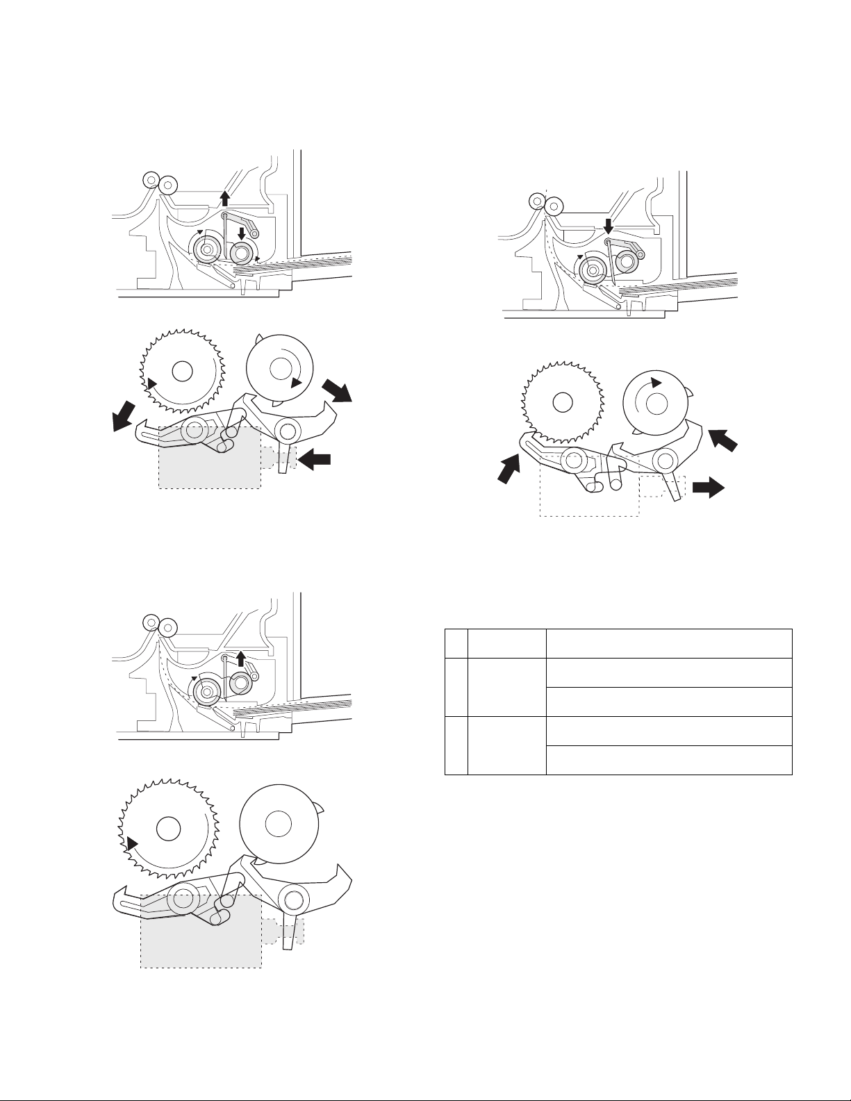
2) When the COPY button is pressed, the main drive motor starts
rotating to drive each drive gear.
The pick-up drive gear also is driven at that time. Since, however,
the paper feed latch is in contact with the projection of the clutch
sleeve, rotation of the drive gear is not transmitted to the pick-up
roller, which does not rotate therefore.
PFS
RRS
OFF
OFF
AR-5012 OPERATIONAL DESCRIPTIONS 7 - 4
Page 29
3) After about 0.1 sec from when the main motor start rotating, the
tray paper feed solenoid (PFS) turns on for a moment.
This disengages the paper feed latch from the projection of the
clutch sleeve, transmitting rotation of the pick-up drive gear to the
paper feed roller shaft, rotating the pick-up roller to feed the paper.
transferred on the paper, which is separated from the OPC drum
by the drum curve and the separation section.
PFS
RRS
OFF
OFF
4) After more than half rotation of the pick-up roller, the paper feed
latch is brought in contact with a notch on the clutch sleeve,
stopping rotation of the pick-up roller.
5) At this time, the paper is fed passed the paper entry detection
switch (PPD1), and detected by it. After about 0.15 sec from
detection of paper by PPD1, the tray paper feed solenoid (PFS)
turns on so that the clutch sleeve projection comes into contact
with the paper feed latch to stop the pick-up roller. Then the pickup roller rotates for about 0.15 sec so that the lead edge of the
paper is evenly pressed on the resist roller, preventing against
skew feeding.
PFS
RRS
OFF
ON
8) The paper separated from the drum is passed through the fusing
paper guide, the heat roller (fusing section), POD (paper out
detector) to the copy tray.
(2) Manual multi paper feed operation
1) Before paper feed operation, the manual paper feed solenoid
(MPFS) is turned OFF as shown in the figure below.
PFS
RRS
ON
OFF
6) To release the resist roller, the tray paper feed solenoid and the
resist solenoid are turned on by the paper start signal to disengage
the resist start latch from the clutch sleeve, transmitting rotation of
the resist drive gear to the resist roller shaft. Thus the paper is
transported by the resist roller.
7) After the resist roller starts rotating, the paper is passed through
the pre-transfer guide to the transfer section. Images are
AR-5012 OPERATIONAL DESCRIPTIONS 7 - 5
OF
F
MPFS
C
A
Page 30
2) When the PRINT button is pressed, the manual paper feed
solenoid (MPFS) turns on to disengage the manual paper feed
latch.
A from the manual paper feed clutch sleeve A, rotating the manual
paper feed roller and the manual take-up roller. At the same time,
the manual paper feed stopper opens and the manual take-up
roller is pressed to the surface of the paper to start paper feeding.
C
4) The lead edge of the transported paper is pressed on the resist
roller by the transport roller. Then the paper is stopped temporarily
to allow synchronization with the lead edge of the image on the
OPC drum.
From this point, the operation is the same as the paper feed
operation from the tray. (Refer to A-5 - 8.)
5) The solenoid turns off to close the gate and return to the initial
state.
A
ON
MPFS
3) When pawl C of the manual paper feed clutch sleeve is engaged
with the manual feed latch, the manual feed stopper falls and the
manual take-up roller rises. At that time, the manual paper feed
roller is rotating.
A
C
OF
F
MPFS
(3) Conditions of occurrence of paper misfeed
a. When the power is turned on:
PPD or POD is ON when the power is turned on.
b. Copy operation
a PPD1 jam PPD1 does not turn off within 4 sec after turning
b PPD2 jam PPD2 is off immediately after turning on the
c POD jam POD does not turn on within 2.9 sec after turning
on the resist roller.
resist roller.
PPD2 does not turn off within 1.2 sec after
turning off the resist roller.
on the resist roller.
POD does not turn off within 1.5 sec - 2.7 sec
after turning off PPD2.
ON
MPFS
A
C
AR-5012 OPERATIONAL DESCRIPTIONS 7 - 6
Page 31
[8] DISASSEMBLY AND ASSEMBLY
(2)
(3)
L
O
C
K
Before disassembly, be sure to disconnect the power cord for
safety.
1. Do not disconnect or connect the connector and the harness
during the machine is powered. Especially be careful not to
disconnect or connect the harness between the MCU PWB
and the LSU (MCU PWB: CN119) during the machine is
powered. (If it is disconnected or connected during the
machine is powered, the IC inside the LSU will be destroyed.)
2. To disconnect the harness after turning on the power, be
sure to turn off the power and wait for at least 10 sec before
disconnection. (Note that a voltage still remains immediately
after turning off the power.)
The disassembly and assembly procedures are described for the following sections:
1. High voltage section
2. Operation panel section
3. Optical section
4. Fusing section
5. Tray paper feed/transport section
6. Manual paper feed section
7. Rear frame section
8. Power section
1. High voltage section
A. List
No. Part name Ref.
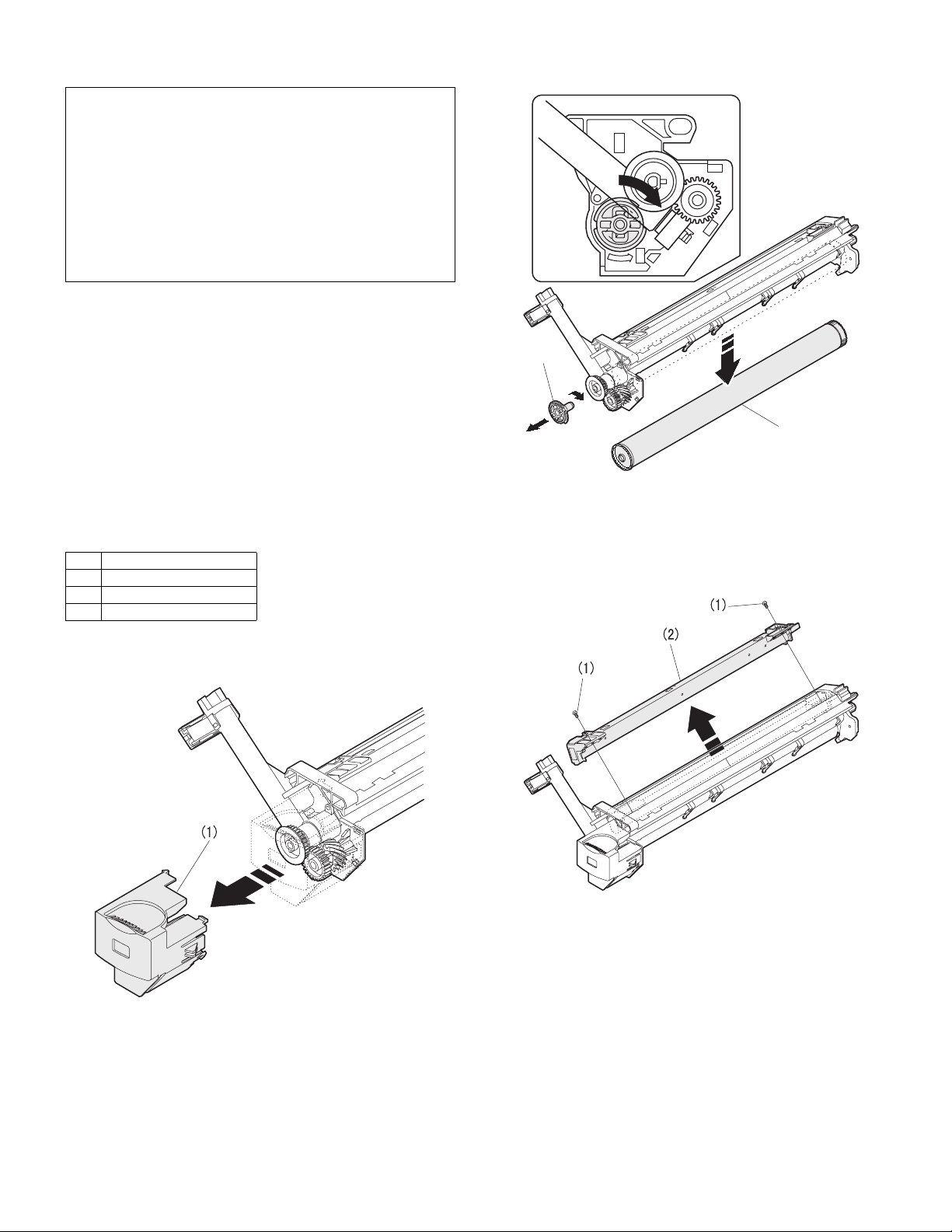
1Drum
2 Transfer charger unit
3 Charger wire
2) Remove the drum fixing plate and the photoconductor drum.
(Note) Dispose the drum fixing plate which was removed.
3) Check the cleaning blade and the red felt for no damage.
• If there is any damage, execute all procedures from item 5) and
later.
• If there is no damage, execute the procedure of item 12).
4) Remove the main charger.
(Cleaning the screen grid and the sawteeth.)
B. Drum replacement
1) Remove the drum cover. (4 Lock Tabs)
AR-5012 DISASSEMBLY AND ASSEMBLY 8 - 1
Page 32

5) Remove the cleaning blade.
Apply grease
(Molykote X5-6020)
Note: Dispose the cleaning blade which was removed.
6) Clean the cleaning section and the waste toner pipe to remove
waste toner completely with a vacuum cleaner.
7) Remove the felt and duplex tape completely.
Note: Be careful not to scratch or bend the sub blade.
8) Attach the cleaning blade.
Securely insert the plate section of the cleaning blade into the unit
and fix it with a screw.
Do not touch the cleaning blade rubber with your hand.
When attaching the cleaning blade, press the cleaning blade in the
arrow direction and attach.
Attach the mocket with slightly pressing section A of the cleaning
blade.
Do not touch the tip of the cleaning blade.
Do not put the mocket under the cleaning blade.
Do not put the mocket on the sub blade.
Do not press the sub blade with the mocket.
10) Attach the main charger.
Securely set the MC holder on the projection of the process frame.
Securely insert two projections of the MC holder into the groove in
the process frame.
When attaching the MC holder ass'y, be careful not to make con-
tact with the cleaning blade.
11) Apply grease to the drum fixing plate.
9) Attach the felt.
Moquette R
0.2 – 0.5 mm
Moquette R
0 – 0.3 mm
∗
Be careful not to allow the
moquette to cover the sub blade.
Example of NG
: Check while pressing the blade.
∗
Cleaning blade
∗
Sub blade
Cleaning blade
Sub blade
0 – 0.3 mm
Moquette F
0 – 0.5 mm0 – 0.5 mm
Attach the drum fixing plate and the photoconductor drum.
0.2 – 0.5 mm
Moquette F
Attach the drum from (b). (Prevention against the sub blade edge
breakage)
Attach the drum so that its position with the sub blade is as shown.
AR-5012 DISASSEMBLY AND ASSEMBLY 8 - 2
Page 33

12) Attach the detection gear.
2)
1)
1)
Transfer
charger
Lock pawl rear
Lock pawl front
Note:
• The detection gear is not installed to the drum cartridge packed
with the main body. Add a new one.
13) Attach the drum cover.
Note: After attaching the drum cover, do not make a copy.
When attaching the drum cover, engage the detection gear
20T rib with the 30T gear rib, and attach the drum cover to
the process frame.
C. Disassembly procedure (Transfer changer unit)
1) Press the side cover open/close button and open the side cover.
2) Push up the lock pawls (2 positions) of the side cover, and remove
the transfer charger.
1)
2)
D. Assembly procedure
For assembly, reverse the disassembly procedure.
E. Charger wire cleaning
1) Remove the charger cleaner from the manual paper feed unit.
1)
AR-5012 DISASSEMBLY AND ASSEMBLY 8 - 3
Page 34
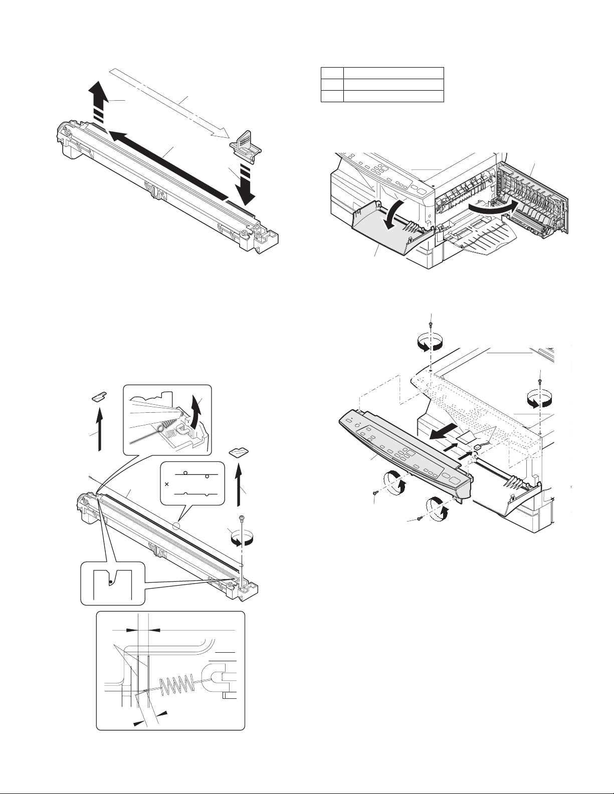
2) Set the charger cleaner to the transfer unit, and move it reciprocally a few times in the direction of the arrow shown in the figure
below.
3)
4)
2)
1)
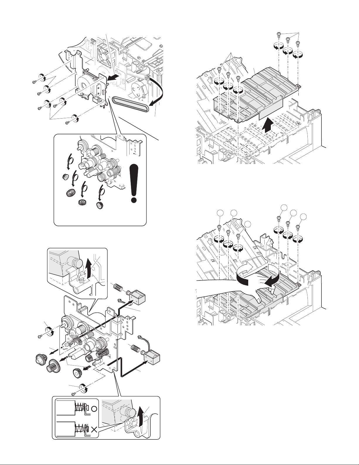
2. Operation panel section
A. List
No. Part name Ref.
1 Operation panel unit
2 Operation PWB
B. Disassembly procedure
1) Open the side door, and Open the front cover.
1)
2)
F. Charger wire replacement
1) Remove the TC cover and remove the screw.
2) Remove the spring and remove the charger wire.
3) Install a new charger wire by reversing the procedures (1) and (2).
At that time, be careful of the following items.
• The rest of the charger wire must be within 1.5mm. Refer to Fig.1
• The spring hook section (charger wire winding section) must be in
the range of the projection section.
• Be careful not to twist the charger wire.
3)
1)
Charger wire
1)
2)
2) Remove the screws (4 pcs.), the harness, and the operation panel
unit.
1)
1)
3)
2)
1)
1)
Protrusion
1mm
1.5mm
Fig.1
AR-5012 DISASSEMBLY AND ASSEMBLY 8 - 4
Page 35

3) Remove four screws, and remove the operation cabinet.
4) Remove four screws, and remove the operation PWB.
1)
2)
1)
3)
2) Remove the four screws, remove the operation unit, and disconnect the connector.
3) Remove the right cabinet.
4) Remove the left cabinet.
5) Remove the screw, and remove the rear cover.
6) Remove the table glass.
1)
6)
7)
1)
3)
3)
4)
3)
3)
5)
4)
1)
Note that there are 10 pawls
C. Assembly procedure
For assembly, reverse the disassembly procedure
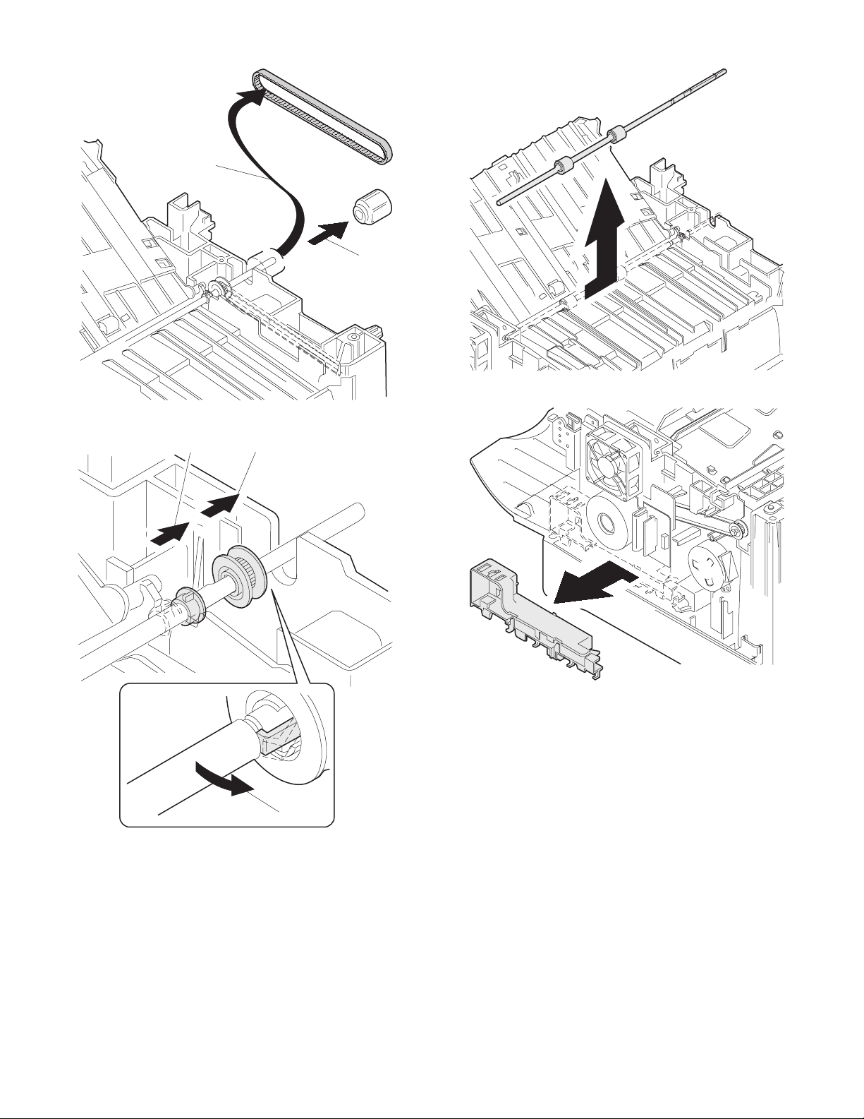
3. Optical section
A. List
NO. Part name Ref.
1 Copy lamp unit
2 Copy lamp
3 Lens unit
5)
8)
4)
1)
3)
2)
1)
1)
7) Move the carriage to the position indicated on the figure.
8) Loosen the screw which is fixing the tension plate.
9) Move the tension plate in the arrow direction to release the tension, and remove the belt.
3)
2)
4)
1)
B. Disassembly procedure
1) Remove four screws, and remove the rear cabinet and the rear
cabinet cover.
1)
1)
2)
1)
AR-5012 DISASSEMBLY AND ASSEMBLY 8 - 5
1)
Page 36

10) Remove the screw, and remove the rod stopper.
Marking line
Note: Attach the FFC
to fit with the marking line.
Note: Attach the FFC to the base
plate securely with duplex tape to
prevent against coming loose.
11) Remove the rod.
3)
2)
1)
12) Lift the rear side of the carriage, remove the belt and the connector, and remove the carriage.
1)
4)
C. Assembly procedure
CCD core
1) Pass the core through the CCD-MCU harness.
2) Insert the CCD-MCU harness into the CCD PWB connector of the
carriage unit.
3) Move the core which was passed through the CCD-MCU harness
near the CCD PWB connector as shown in the figure below, and fix
it with a filament tape (19mm wide, 40mm long). For the attachment reference, refer to the figure below. Clean and remove oil
from the attachment section.
4) Attach the CCD-MCU harness to the duplex tape on the back of
the carriage unit.
5) Attach the PWB holder to the position specified in the figure below.
6) Pass the core through the FFC and the PWB holder, and fix the
core.
2)
3)
AR-5012 DISASSEMBLY AND ASSEMBLY 8 - 6
Page 37

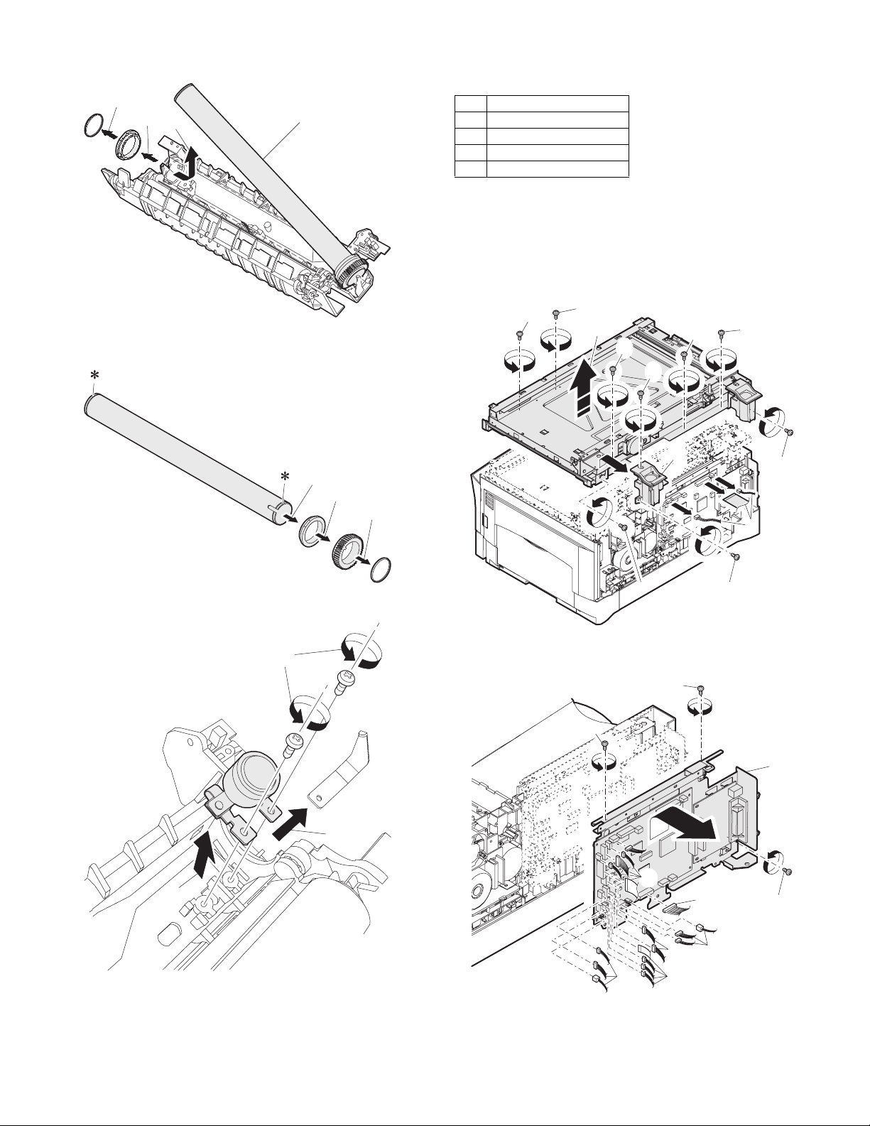
4. Fusing section
1)
2)
1)
5)
5)
6)
6)
4)
3)
2)
1)
2)
PPD2 sensor
A. List
No. Part name Ref.
1 Thermistor
2 PPD2 sensor
3 Heater lamp
4 Pressure roller
5 Heat roller
B. Disassembly procedure
1) Remove the connectors (3 pcs.) of the rear cabinet.
2) Open the side cover, remove two screws, and remove the fusing
unit.
1)
4) Remove the screw and remove the U-turn guide.
Pressure roller section disassembly
5) Remove the three screws, remove the fusing cover lower on the
right side, and open the heat roller section.
3)
2)
3) Cut the binding band, remove the screw, and remove the thermistor.
2)
2)
Thermistor
3)
6) Remove the screw and remove the PPD2 sensor.
1)
AR-5012 DISASSEMBLY AND ASSEMBLY 8 - 7
Page 38

7) Remove the plate spring on the right and remove the heater lamp.
1)
1)
1)
2)
2)
1)
3)
3)
Pressure roller
1)
2)
Heater lamp
8) Remove the spring and remove the separation pawls (3 pcs.).
10) Remove the pressure release levers on the right and the left sides.
11) Remove the pressure roller, the pressure bearing, and the spring.
Note: Apply grease to the sections specified with an asterisk (*).
3)
2)
1)
9) Remove the E-ring and remove the reverse gate.
3)
1)
Heat roller disassembly
(Continued from procedure (4).)
5) Remove screws, remove the fusing cover, and open the heat roller
section.
3)
2)
2)
3)
1)
2)
AR-5012 DISASSEMBLY AND ASSEMBLY 8 - 8
Page 39
6) Remove the C-ring and the fusing bearing, and remove the heat
roller.
1)
2)
3)
Heat roller
5. Tray paper feed/transport section
A. List
No. Part name Ref.
1 PPD1 sensor PWB
2 LSU unit
3 Intermediate frame unit
4 Paper feed roller
B. Disassembly procedure
1) Remove two screws, and remove the hinge guide R.
2) Disconnect three positions of the connectors.
3) Remove six screws, and remove the scanner unit.
4) Remove the fan duct.
7) Remove the parts from the heat roller.
Note: Apply grease to the sections specified with *.
3)
8) Remove two screws and remove the thermo unit.
1)
4)
4)
5)
4)
1)
4)
2)
4)
4)
2
1)
3)
4)
4) Remove each connector and three screws, and remove the MCU
PWB.
2)
1)
3)
C. Assembly procedure
For assembly, reverse the disassembly procedure.
2)
AR-5012 DISASSEMBLY AND ASSEMBLY 8 - 9
2)
3)
1)
1)
1)
1)
1)
1)
2)
Page 40

5) Remove the PWB insulation mylar and remove the paper transport
4)
2)
1)
3)
detection sensor (PPD2).
7) Remove two springs and open the intermediate frame unit.
1)
3)
2)
6) Remove two screws and remove the toner motor.
1)
2)
8) Remove the pulleys on the both sides and remove the paper exit
roller.
1)
2)
AR-5012 DISASSEMBLY AND ASSEMBLY 8 - 10
Page 41
9) Pull out the paper exit roller knob and remove the belt.
2)
1)
10) Release the belt pulley (a) lock and remove the belt pulley bearing.
11) Remove the paper exit roller.
12) Remove the harness guide.
3)
2)
1)
AR-5012 DISASSEMBLY AND ASSEMBLY 8 - 11
Page 42
13) Remove five screws and remove the main drive plate and the belt.
1)
1)
2)
1
3
5
2 4
6
2)
1)
15) Remove six screws and remove the LSU unit.
1)
3)
CAUTION:Attach the gears securely
14) Remove the parts as shown below, and remove the pressure
release solenoid and the paper feed solenoid.
3)
[Note for assembling the LSU]
When installing the LSU, turn the LSU clockwise and fix with
screws in order to provide an attachment backlash in the proper
direction.
Observe the following sequence of fixing screws.
4)
2)
1)
1)
2)
4)
3)
AR-5012 DISASSEMBLY AND ASSEMBLY 8 - 12
Page 43
16) Remove each pawl, and remove the paper exit tray.
5)
4)
4)
1)
2)
3)
PS roller unit
PS semi-circuler
earth plate
5)
4)
4)
1)
2)
3)
PS roller unit
PS semi-circular
earth plate
3)
19) Remove the screw and the E-ring, and remove the PS semi-circular earth plate and the PS roller unit.
2)
20) Remove three screws and remove the TC front paper guide.
1)
2)
1)
17) Remove two screws and remove the fusing connector.
18) Remove five screws and the connector, and lift the intermediate
frame unit to remove.
3)
4)
2)
2)
21) Remove the E-ring and remove the spring clutch from the PS roller
unit.
1)
AR-5012 DISASSEMBLY AND ASSEMBLY 8 - 13
Page 44

22) Remove the screw and the connector, and remove the PPD1 sen-
1)
2)
Back Wire treatment
sor PWB.
1)
2)
23) Remove two E-rings and remove the paper feed roller.
24) Remove three E-rings and remove the clutch unit.
6. Manual paper feed section
A. List
No. Part name Ref.
1 Manual transport roller
2 Cassette detection switch
3 PPD1 sensor PWB
4 Side door detection unit
B. Disassembly procedure
Single unit
1) Remove the screw and remove the single upper cover.
1)
5)
Paper feed
roller
4)
3)
Back
2)
Clutch unit
4)
Front
1)
2) Remove the screw and remove the side door detection unit.
C. Assembly procedure
For assembly, reverse the disassembly procedure.
2)
AR-5012 DISASSEMBLY AND ASSEMBLY 8 - 14
Page 45

3) Remove three screws and remove the single manual feed upper
3)
3)
4)
1)
2)
1)
2)
3)
Wire treatment
frame.
1)
1)
2)
5) Remove the E-ring and remove the manual paper feed transport
roller.
6) Remove the cassette detection switch.
4) Remove the PPD1 sensor PWB.
3)
1)
2)
Wire treatment
AR-5012 DISASSEMBLY AND ASSEMBLY 8 - 15
Page 46

7) Remove the multi cover.
1)
2)
3)
1)
2)
3)
1)
2)
3)
Multi cover
7. Rear frame section
A. List
No. Part name Ref.
1 Mirror motor
2 Main motor
3 Exhaust fan motor
2) Disconnect the connector.
3) Remove two screws, and remove the scanner motor.
4) Remove two screws and one harness, and remove the main
motor.
B. Disassembly procedure
1) Remove four screws, and remove the rear cabinet and the rear
cabinet cover.
1)
1)
2)
1)
1)
5) Remove two screws and one connector, and remove the exhaust
fan motor.
C. Assembly procedure
AR-5012 DISASSEMBLY AND ASSEMBLY 8 - 16
For assembly, reverse the disassembly procedure.
Page 47

8. Power section
A. List
No. Part name Ref.
1 Noise filter PWB
2 Power PWB
B. Disassembly procedure
Noise filter PWB
1) Disconnect the connector at two positions.
2) Remove the screw, and remove the noise filter PWB unit.
2)
1)
3)
1)
Power PWB
1) Disconnect each connector.
2) Remove the screw, and remove the earth line.
3) Remove two screws, and remove the power PWB unit.
4)
1)
1)
2)
3)
5)
1)
1)
4)
1)
C. Assembly procedure
For assembly, reverse the disassembly procedure.
AR-5012 DISASSEMBLY AND ASSEMBLY 8 - 17
Page 48
[9] ADJUSTMENTS
1. Optical section
A. Copy magnification ratio adjustment
The copy magnification ratio must be adjusted in the main scanning
direction and in the sub scanning direction. To adjust, use SIM 48-1.
(1) Outline
The main scanning (front/rear) direction magnification ratio adjustment
is made automatically or manually.
Automatic adjustment: The width of the reference line marked on the
shading correction plate is scanned to perform the main scanning
(front/rear) direction magnification ratio adjustment automatically.
Manual adjustment: The adjustment is made by manual key
operations. (In either of the automatic and manual adjustments, the
zoom data register set value is changed for adjustment.)
The magnification ratio in the sub scanning direction is adjusted by
changing the carriage (scanner) scanning speed.
(2) Main scanning direction magnification ratio adjustment
a. Cases when the adjustment is required
1) When the main PWB is replaced.
2) When the EEPROM in the main PWB is replaced.
3) When "U2" trouble occurs.
4) When repairing or replacing the optical section.
b. Necessary tools
• Screwdriver (+)
• Scale
c. Adjustment procedure
Automatic adjustment
In the first place, perform SIM48-1 (Main scanning direction
magnification ratio adjustment and black level correction (CCD dark
component target value setup)).
To perform the automatic adjustment, place the gray gradation chart
(UKOG-0162FCZZ) face down so as to fit with the left center of the
platen with the darker side (Density 10) on the left of OC.
Manual adjustment
1) Set the scale vertically on the document table. (Use a long scale
for precise adjustment.)
2) Set the copy magnification ratio to 100%.
3) Make a copy on A4 or 81/2" x 11" paper.
4) Measure the length of the copied scale image.
5) Calculate the main scanning direction magnification ratio.
Main scanning direction magnification ratio
Copy image dimensions
=
Original dimension
(When a 100mm scale is used as the original.)
mm
20
10
1/2mm
Paper feed
direction
mm
1/2mm
Reference
10 20
X 100 (%)
100 110 120 130
100
Comparison point
JAPAN
JAPAN
110
120 130
140
140
Original (Scale)
HARDENED
STAINLESS
150
Shizuoka
HARDENED
STAINLESS
150
Shizuoka
Copy
110
10 1
Back of the chart
In the case of the automatic adjustment, when the PRINT switch is
pressed, the mirror base unit moves to the white plate for shading to
scan the width of the reference line, calculating the correction value
and displaying and storing this value.
After completion of the automatic adjustment, press the density
adjustment Down key, and the black level will be displayed in
hexadecimal number (3 digits) of 12bits.
After execution of the automatic adjustment, go out from the simulation
mode and make a copy to check the magnification ratio.
Adjustment mode Lighting lamp
Main scanning direction auto copy
Auto exposure lamp ON
magnification ratio adjustment and
black level automatic correction
Main scanning direction manual copy
Manual exposure lamp ON
magnification ratio adjustment
Sub scanning direction copy
Photo exposure lamp ON
magnification ratio adjustment
SPF mode scanning direction
magnification ratio adjustment
Auto, Manual, Photo lamp
ON
AR-5012 ADJUSTMENTS 9 - 1
6) Check that the copy magnification ratio is within the specified
range. If it is not within the specified range, perform the following
procedures.
7) Execute SIM 48-1 to select the main scanning direction copy
magnification ratio adjustment mode.
To select the adjustment mode, use the copy mode select key.
If the magnification ratio is not in the specified range (100±1.0%),
manually adjust as follows.
8) Set the adjustment mode to Manual with the copy mode select key.
9) Enter the new set value of main scanning direction copy
magnification ratio with the copy quantity set key, and press the
COPY button.
10) Change the set value and repeat the adjustment until the ratio is
within the specified range.
When the set value is changed by 1, the magnification ratio is
changed by 0.1%.
(3) Sub scanning direction copy magnification ratio
a. Cases when the adjustment is required
1) When the scanner unit drive section is disassembled or the part is
replaced.
2) When the main PWB is replaced.
3) When the EEPROM in the main PWB is replaced.
4) When "U2" trouble occurs.
Page 49

b. Necessary tools
• Scale
c. Adjustment procedure
1) Set the scale on the document table as shown below. (Use a long
scale for precise adjustment.)
2) Set the copy magnification ratio to 100%.
3) Make a copy on A4 or 81/2" x 11" paper.
4) Measure the length of the copied scale image.
5) Calculate the sub scanning direction copy magnification ratio
using the formula below.
Copy image dimensions
=
Original dimension
X 100 (%)
110
Original (Scale)
HARDDENCD
mm
1/2mm
mm
1/2mm
Reference
10 20
10
100
20
100
Comparison point
JAPAN
110 120 130
JAPAN
110 120
130
STAINLESS
140
150
Shizuoka
HARDDENCD
STAINLESS
140
150
Shizuoka
Copy
Paper feed
direction
6) Check that the actual copy magnification ratio is within the
specified range. (100 ± 1.0%).
If it is not within the specified range, perform the following
procedures.
7) Execute SIM 48-1 to select the sub scanning direction copy
magnification ratio adjustment mode.
To select the adjustment mode, use the copy mode select key.
(Photo exposure lamp ON)
8) Enter the new set value of sub scanning direction copy
magnification ratio with the copy quantity set key, and press the
COPY button.
Repeat procedures 1) - 8) until the sub scanning direction actual copy
magnification ratio in 100% copying is within the specified range.
When the set value is changed by 1, the magnification ration is
changed by 0.1%.
B. Image position adjustment
There are following five kinds of image position adjustments, which are
made by laser control except for the image scan start position
adjustment. For the adjustments, SIM 50 - 01, 50 - 10, 50 - 18 and SIM
50 - 19 are used.
No. Adjustment item Simulation
1 Print start position 50 - 01
2 Image lead edge void amount 50 - 01
3 Image scan start position 50 - 01
4 Image rear edge void amount 50 - 01
5 SPF image scan start position 50 - 01
6 Center offset 50 - 10
7 Memory reverse position adjustment in
duplex copy
8 Duplex copy rear edge void adjustment 50 - 19
9 Duplex back print start position 50 - 19
To select the adjustment mode with SIM 50 - 01, use the copy mode
select key.
The relationship between the adjustment modes and the lighting lamps
are as shown in the table below.
Adjustment mode Lamp ON
Print start position (Main cassette paper
AE, main cassette lamp
feed)
Print start position (2nd cassette paper
AE, 2nd cassette lamp
feed)
Print start position (Manual paper feed) AE, manual feed lamp
Image lead edge void quantity TEXT lamp
Image scan start position PHOTO lamp
Image rear edge void quantity AE, TEXT, PHOTO
lamp
SPF image scan start position AE, TEXT lamp
: Supported for the installing model and skipped for non-installing
mode.
To select the adjustment mode with SIM 50 - 10, use the copy mode
select key.
The relationship between the adjustment modes and the lighting lamps
are as shown in the table below.
Machine with the multi manual paper feed unit
Adjustment mode Lamp ON
Print center offset (Main cassette paper
AE, main cassette lamp
feed)
Print center offset (Manual paper feed) AE, manual paper feed lamp
OC/document center offset AE, TEXT lamp
Machine with the single manual paper feed unit
Adjustment mode Lamp ON
Print center offset (Main cassette paper
AE, main cassette lamp
feed)
Print center offset (Manual paper feed) AE, manual paper feed lamp
OC/document center offset AE, TEXT lamp
Duplex copy rear edge void adjustment mode
Adjustment mode Lamp ON
Image cut rear edge void quantity
AE lamp
(RSPF)
Paper rear edge void quantity TEXT lamp
Print start position (Duplex back) PHOTO lamp
RSPF (Back) original center offset AE, TEXT, PHOTO lamps
50 - 18
AR-5012 ADJUSTMENTS 9 - 2
Page 50
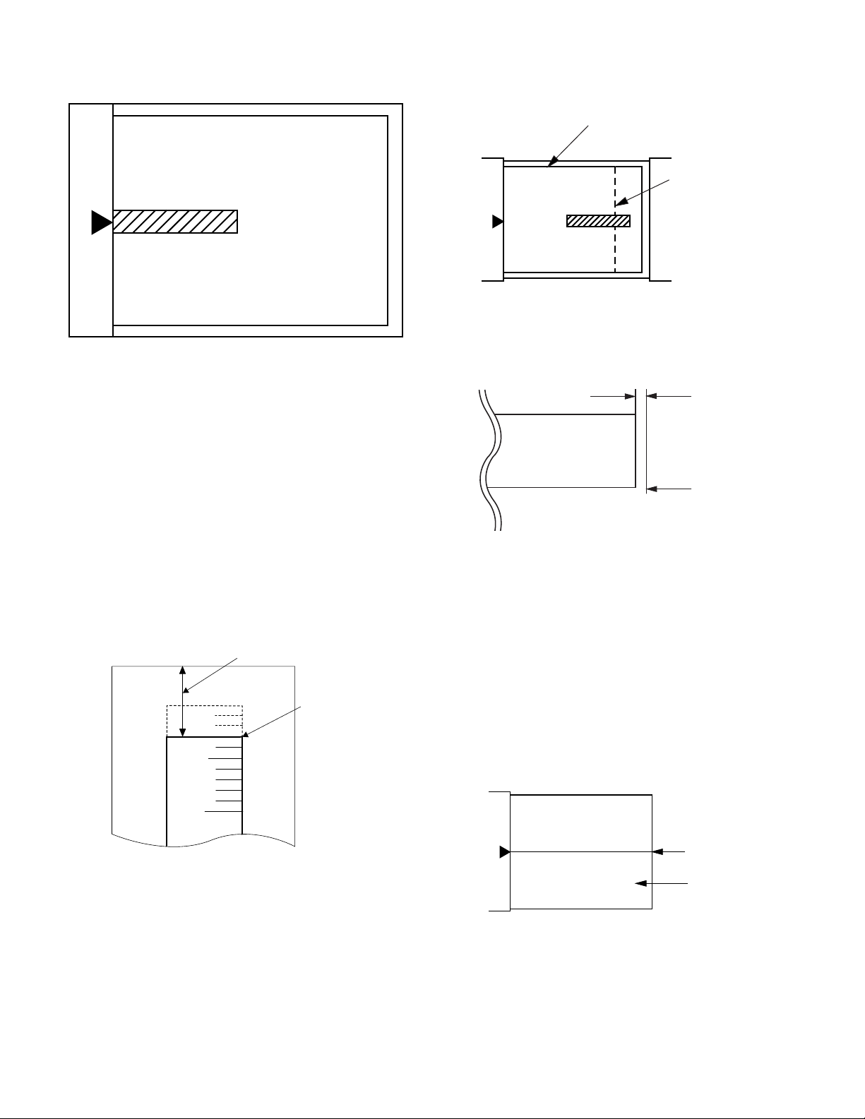
(1) Lead edge adjustment
1) Set a scale to the center of the paper lead edge guide as shown
below, and cover it with B4 or 8 1/2" x 14" paper.
2) Execute SIM 50 - 01
3) Set the print start position (AE lamp ON) (A), the lead edge void
amount (TEXT lamp ON) (B), and the scan start position (PHOTO
lamp ON) (C) to 0, and make a copy of a scale at 100%.
4) Measure the image loss amount (R mm) of the scale image.
Set C = 10 X R (mm). (Example: Set the value of C to 30.)
When the value of C is increased by 10, the image loss is
decreased by 1mm. (Default: 50)
5) Measure the distance (H mm) between the paper lead edge and
the image print start position.
Set A = 10 X H (mm). (Example: Set the value of A to 50.)
When the value of A is increased by 10, the image lead edge is
shifted to the paper lead edge by 1mm. (Default: 50)
6) Set the lead edge void amount to B = 50 (2.5mm).
When the value of B is increased by 10, the void amount is
increased by about 1mm. For 25 or less, however, the void amount
becomes zero. (Default: 50)
(Example)
Distance between paper lead
edge and image: H = 5mm
Image loss:
R = 3mm
5mm
(2) Image rear edge void amount adjustment
1) Set a scale to the rear edge section of A4 or 11" x 8 1/2" paper size
as shown in the figure below, and cover it with B4 or 8 1/2" x 14"
paper.
B4 or 8 1/2″ × 14″ paper
A4 size rear edge
2) Execute SIM 50 - 01 to select the image rear edge void amount
adjustment mode.
The set adjustment value is displayed on the copy quantity display.
3) Make a copy and measure the void amount of image rear edge.
Void amount (Standard value: 2 3mm)
Scale image
Paper rear edge
4) If the measurement value is out of the specified range, change the
set value and repeat the adjustment procedure.
The default value is 50.
Note: The rear edge void cannot be checked with the first sheet after
entering the simulation mode, the first sheet after turning off/on
the power, or the first sheet after inserting the cassette. Use the
second or later sheet to check the rear edge void.
(3) Center offset adjustment
1) Set the self-made test chart for the center position adjustment so
that its center line is aligned with the center mark of the document
guide.
• Test chart for the center position adjustment.
Draw a line at the center of A4 or 8 1/2" x 11" paper in the paper
transport direction.
Document guide
10mm
2) Execute SIM 50 - 10 to select the print center offset (cassette
paper feed) adjustment mode.
The set adjustment value is displayed on the copy quantity display.
AR-5012 ADJUSTMENTS 9 - 3
Center
Copy paper
(A4 or 8 1/2″ × 11″)
Page 51

3) Make a copy and check that the copied center line is properly
positioned.
The standard value is 0 ±2mm from the paper center.
(Copy A)
(Copy B)
2.0mm or less
Shift
2.0mm or less
Copy image
Copy paper
folding line
Copy image
Test chart comparison table
UKOG0162FCZZ
DENSITY
12345678910W
No.
UKOG0089CSZZ
DENSITY
0.1 0.2 0.3 0.5 1.9 0
No.
KODAK
GRAY
123419A
SCALE
Shift
(Paper feed direction)
Copy paper
folding line
4) If the measured value is out of the specified range, change the set
value and repeat the adjustment procedure.
When the set value is increased by 1, the copy image is shifted by
0.1mm toward the rear frame.
• For the manual paper feed, change the manual paper feed
adjustment mode and perform the similar procedures.
• Since the document center offset is automatically adjusted by the
CCD which scan the reference lines (F/R) on the back of document
guide, there is no need to adjust manually.
2. Copy density adjustment
A. Copy density adjustment timing
The copy density adjustment must be performed in the following cases:
• When maintenance is performed.
• When the developing bias/grid bias voltage is adjusted.
• When the optical section is cleaned.
• When a part in the optical section is replaced.
• When the optical section is disassembled.
• When the OPC drum is replaced.
• When the main control PWB is replaced.
• When the EEPROM on the main control PWB is replaced.
• When the memory trouble (U2) occurs.
B. Note for copy density adjustment
1) Arrangement before execution of the copy density adjustment
• Clean the optical section.
• Clean or replace the charger wire.
• Check that the voltage at the high voltage section and the
developing bias voltage are in the specified range.
C. Necessary tool for copy density adjustment
• One of the following test charts:
UKOG-0162FCZZ, UKOG-0089CSZZ, KODAK GRAY SCALE
• B4 (14" x 8 1/2") white paper
• The user program AE setting should be "3."
1 10
23456789
W
D. Features of copy density adjustment
For the copy density adjustment, the image data shift function provided
in the image process LSI is used.
List of the adjustment modes
Auto Mode Brightness 1 step only
Manual Mode Brightness 5 steps. Adjustment of only the center
brightness is made.
Photo Mode Brightness 5 steps. Adjustment of only the center
brightness is made.
Manual T/S
mode
Brightness 5 steps. Adjustment of only the center
brightness is made.
T/S Auto mode Brightness 1 step only
E. Copy density adjustment procedure
Use SIM 46 - 01 to set the copy density for each copy mode.
For selection of modes, use the copy mode select key.
(1) Test chart (UKOG-0162FCZZ) setting
1) Place the test chart so that its edge is aligned with the A4 (Letter)
reference line on the document table. Then place a A4 (14" x
8 1/2") white paper on the test chart and close the document cover.
White paper
Test chart
AR-5012 ADJUSTMENTS 9 - 4
Page 52

(2) Perform the adjustment in each mode.
1) Execute SIM 46-1.
2) Select the mode to be adjusted with the exposure mode select key.
Set the exposure level to 3 for all adjustment. (Except for the auto
mode.)
(1)
(2)
(1) Mode select key/display
lamp
(2) Exposure level select
key/display lamp
Adjustment mode
Exposure mode
display lamp
Auto mode Auto lamp ON "3" is slightly copied.
Manual mode Manual lamp ON "3" is slightly copied.
Photo mode Photo lamp ON "3" is slightly copied.
Manual T/S mode Manual lamp/Photo lamp ON"3" is slightly copied.
Auto T/S mode Auto lamp/Photo lamp ON "3" is slightly copied.
3) Make a copy.
Check the adjustment level (shown in the above table) of the
exposure test chart (Sharp Gray Scale).
Sharp Gray Scale adjustment level
Non toner
save mode
1 10
23456789
Sharp gray chart
adjustment level
W
3. High voltage adjustment
A. Main charger (Grid bias)
Note:
• Use a digital multi meter with internal resistance of 10MΩ or more
measurement.
• After adjusting the grid LOW output, adjust the HIGH output. Do not
reverse the sequence.
Procedures
1) Set the digital multi meter range to DC700V.
2) Set the positive side of the test rod to the connector CN11-3
(GRID) of high voltage section of the power PWB and set the
negative side to the frame ground (power frame).
3) Execute SIM 8-3. (The main charger output is supplied for 30 sec
in the grid voltage LOW output mode.)
Adjust the control volume (VRG2) so that the output voltage is
4)
–390 ±20V.
5) Execute SIM 8-2. (The main charger output is supplied for 30 sec
in the grid voltage HIGH output mode.)
6) Adjust the control volume (VRG1) so that the output voltage is 580
±12V.
VRG1
VRG2
Slightly copied.
Not copied.
Toner save
mode
1 10
23456789
Slightly copied.
Not copied.
W
(When too bright): Decrease the value displayed on the copy quantity
display.
(When too dark): Increase the value displayed on the copy quantity
display.
* The value can be set in the range of 1 - 99.
B. DV bias check
Note: • A digital multi meter with internal resistance of 1GΩ must be
use for correct check.
• The adjustment volume is locked, and no adjustment can be
made.
Procedures
1) Set the digital multi meter range to DC500V.
2) Set the positive side of the test rod to the connector CN-10-1 (DV
BIAS) and set the negative side to the frame ground (power
frame).
3) Execute SIM 25-1 to output the developing bias for 30sec, and
check that the output is –400 ±8V.
VRDV
AR-5012 ADJUSTMENTS 9 - 5
Page 53

[10] SIMULATION, TROUBLE CODES
1. Entering the simulation mode
To enter the serviceman simulation mode, press the keys as follows:
Clear → Density select → Clear→ Density select
To cancel the simulation mode, press the clear key.
Flow chart of entering the simulation mode
1
The current set adjustment
value and the counter
value are displayed on the
COPY QUANTITY
displayed Sensor check,
etc. are displayed by the
alarm lamps, etc.
To change the current set
values, enter with the COPY
QUANTITY key.
10th digit:
1st digit:
Count up of values:
COPY QUANTITY key
Count down of values:
Zoom key + COPY
QUANTITY key
The entered value
is displayed on the
COPY QUANTITY
display.
Press the COPY
key.
Is there a sub
code ?
NO
Press the COPY
key.
Is it the
simulation for
operation
check?
YES
Perform the operation
according to the
simulation number.
Is another
simulation to be
performed ?
NO
Press the clear key.
All displays on the
operation panel go off,
and the machine enters
the ready state for
entering the main code.
YES
YES
Press the COPY key.
The COPY QUANTITY
display blinks to indicate
"00" and the machine
enters the ready
state for sub code input.
Enter the sub code with
the COPY QUANTITY key.
10th digit
1st digit:
Count up of values:
COPY QUANTITY key
Count down of values:
Zoom key + COPY
QUANTITY key
Press the COPY key.
Is the
main code the
same ?
NO
Is the
sub code
displayed ?
YES
Press the clear key.
The COPY QUANTITY
display blinks to indicate
the previously set sub
enters the ready 7 state for
sub code input.
code, and the machine
YES
Press the clear key.
NO
Enter the new main
code.
The main code is
displayed on the
COPY QUANTITY
display.
Start
Press the clear key.
Within 1sec
Press the exposure
mode selector key.
Within 1sec
Press the clear key.
Within 1sec
Press the exposure
mode selector key.
All displays on the
operation panel go off,
and the machine enters
he ready state for entering
he main code.
Enter the main code with
the COPY QUANTITY key.
10th digit:
1st digit:
Count up of values:
COPY QUANTITY key
Count down of values:
Zoom key + COPY
QUANTITY key
The main code is
displayed on the
COPY QUANTITY
display.
The entered value
is registered.
1
Press the clear key.
End
AR-5012 SIMULATION, TROUBLE CODES 10 - 1
Page 54

2. List of simulations
Sim
No.
01 Optical system 01 Mirror scan operation
05 Lamp ON
06 Machine
07 Aging 01 Warm-up display and aging with jam
08 High voltage
10 Other None Toner motor aging
14 Trouble reset None Cancel of troubles other than U2
16 U2 trouble
20 01 Maintenance counter clear
21 01 Maintenance cycle setup
22 Counter
24 Special
25 Main motor
Kind of
main code
check
individual load
operation
output check
reset
display
counter clear
ON
Sub
code
06 Aging of mirror scanning
01 Operation panel display check
02 Fusing lamp, cooling fan operation
check
03 Copy lamp ON
01 Paper feed solenoid ON
02 Resist solenoid ON
06 Intermittent aging
01 Developing bias
02 Main charger (Grid high)
03 Grid voltage (Low)
06 Transfer charger
None Cancel of U2 trouble
02 Mini maintenance cycle setup (Valid
only when the destination is set to
Japan AB series.)
01 Maintenance counter display
02 Maintenance preset value display
04 JAM total counter display
05 Total counter display
06 Developer counter display
12 Drum counter display
14 P-ROM version display
17 Copy counter display
19 Scanner mode counter display
21 Scanner counter display
01 JAM total counter clear
06 Developer counter clear
07 Drum counter clear
08 Copy counter clear
13 Scanner counter clear
15 Scanner mode counter clear
01 Main motor operation check (Cooling
fan motor rotation check)
10 Polygon motor ON
Operation
Sim
No.
26 Various setup 01 Manual feed setup
30 Sensor
43 Fusing
46 Exposure
48 Magnification
49 01 Flash ROM program writing mode
50 Lead edge
51 Timing
61 Laser system
63 Shading 01 Shading check
64 Self print 01 Self print
Kind of
main code
operation
check
(Standard
provision)
temperature
setup
adjustment
ratio correction
and black level
adjustment
adjustment
adjustment
operation
Sub
code
02 (R) SPF setup
03 Second cassette setup
04 Machine duplex setup
06 Destination setup
07 Machine conditions check
20 Rear edge void setup
30 CE mark support control ON/OFF
37 Developer life-over termination
cancel
38 Cancel of stop at drum life over
39 Memory capacity check
40 Polygon motor OFF time setup
(Time required for turning OFF after
completion of printing)
42 Transfer ON timing control setup
43 Side void setup
55 CRUM Destination Indication
62 Energy-save mode copy lamp setup
63 Fan control select setup
64 Heater control setup during the
scanner mode
01 Paper sensor status display
01 Fusing temperature setup (Normal
copy)
04 Fusing temperature setup 2
05 Fusing temperature setup in duplex
copy
09 Setup of fusing control of postcard
size paper
01 Copy density adjustment (300dpi)
02 Copy density adjustment (600dpi)
18 Image contrast adjustment (300dpi)
19 γ table setup or AE operation mode
setup
29 Image contrast adjustment (600dpi)
31 Image sharpness adjustment
32 Copier color reproduction setup
01 Front/rear (main scanning) direction
and scan (sub scanning) direction
magnification ratio adjustment and
black level adjustment
01 Lead edge image position
10 Center offset adjustment
02 Resist quantity adjustment
03 Polygon motor check
(HSYNC output check)
Operation
AR-5012 SIMULATION, TROUBLE CODES 10 - 2
Page 55

3. Contents of simulations
Input method: Clear key → Exposure Select key → Clear key → Exposure Select key
Main
Sub
code
code
01 01 Mirror scan operation
(Operation/Procedure)
1. When this simulation is executed, the mirror home position is detected.
Sensor name Display lamp
Mirror home position sensor Developer replacement lamp
2. When the _START key is pressed, scanning is executed at the speed corresponding to the currently set copy magnification ratio.
The copy magnification ratio can be arbitrarily set with the magnification ratio select key/zoom key.
06 Aging of mirror scanning
When the PRINT switch is pressed, the mirror base performs full scan at the speed of the set magnification ratio. After 3 sec, the mirror
case performs full scan again. These procedures are repeated until the clear key is pressed. (When the PRINT switch is pressed once,
the ready lamp keeps OFF.)
The status of the mirror home position sensor is displayed with the photoconductor cartridge lamp. (The lamp is ON when the mirror is
at the home position.)
During aging, the copy lamp keeps ON.
05 01 Operation panel display check
06 01 Paper feed solenoid ON
07 01 Warm-up display and aging with jam
• When the PRINT switch is pressed, all LEDs (including 7-segment LEDs) on the operation panel are lighted. (LED check mode)
• When 1Up key is pressed, the LEDs on the operation panel are lighted individually from the top left to the bottom right in sequence.
After completion of all individual lighting, all LEDs are lighted simultaneously. (The 7-segment LED lights the three-digit sections at
the same time.)
Individual lighting frequency ON: 300ms, OFF: 20ms
• When the CLEAR key is pressed, this simulation is terminated.
• When the PRINT switch is pressed in the LED check mode, the machine enters the Key input check mode.
“Key input check mode”
When the machine enters the Key input check mode, the value display section indicates “– – –.” Every time any key on the operat ion
panel is pressed, the entered value is added and displayed on the value display section. However, the keys that were pressed once are
not counted again.
• When the PRINT switch is pressed, the entered value is added and displayed for 3 sec and all the LEDs are lighted. (LED lighting
check mode)
(Note for Key input check mode)
• Press the PRINT switch at the end. (If it is pressed in the middle of the process, the entered value up to that moment is displayed for
3 sec and the machine enters the LED lighting check mode. (ALL the LEDs are lighted.))
• Multiple key inputs are ignored.
02 Fusing lamp, cooling fan operation check
When the PRINT switch is pressed, the fusing lamp repeats operations of 500ms-ON and 500ms-OFF 5 times. During that time, the
cooling fan motor rotates.
03 Copy lamp ON
(Operation/Procedure)
When the START key is pressed, the copy lamp is lighted for 5 sec.
(Operation/Procedure)
When the START key is pressed, the paper feed solenoid selected by the tray select key repeats ON (500ms) and OFF (500ms) 20
times.
02 Resist solenoid ON
(Operation/Procedure)
When the START key is pressed, the resist solenoid (RRS) repeats ON (500ms) and OFF (500ms) 20 times.
(Operation/Procedure)
1. When the simulation is executed, warming up is started.
2. Warm-up time is counted and displayed every second on the copy quantity display.
3. After completion of warm-up, the time count is stopped and the ready lamp is lighted.
4. Press the clear key to clear the warm-up time display, set the copy quantity, and press the START key, and the machine will copy
the set quantity repeatedly.
This simulation is canceled by turning off the power or executing any simulation which performs hardware reset.
06 Intermittent aging
(Operation/Procedure)
1. When the simulation is executed, warming up is started.
2. After completion of warm-up, the ready lamp is lighted.
3. Set the copy quantity and press the START key, and the machine will copy the set quantity repeatedly.
4. After 3 sec of the interval time from completion of copying the set quantity, the machine will resume copying.
5. The above operation 4 is repeated.
This simulation is canceled by turning off the power or executing any simulation which performs hardware reset.
Content
AR-5012 SIMULATION, TROUBLE CODES 10 - 3
Page 56

Main
Sub
code
code
08 01 Developing bias
(Operation/Procedure)
When the START key is pressed, the developing bias is outputted for 30 sec.
02 Main charger (Grid high)
(Operation/Procedure)
When the START key is pressed, the main charger output is supplied for 30 sec in the grid voltage HIGH mode.
03 Grid voltage (Low)
(Operation/Procedure)
When the START key is pressed, the main charger output is supplied for 30 sec in the grid voltage LOW mode.
06 Transfer charger
(Operation/Procedure)
When the START key is pressed, the transfer charger output is supplied for 30 sec.
10 None Toner motor aging
(Operation/Procedure)
When the START key is pressed, the toner motor output is supplied for 30 sec.
14 None Cancel of troubles other than U2
(Operation/Procedure)
After canceling the trouble, the simulation is also automatically canceled.
16 None Cancel of U2 trouble
(Operation/Procedure)
1. When the START key is pressed, the EEPROM total counter check sum is rewritten and the trouble is canceled.
2. After canceling the trouble, the simulation is also automatically canceled.
20 01 Maintenance counter clear
When the PRINT switch is pressed, the maintenance count is cleared and the value “000000” is displayed.
21 01 Maintenance cycle setup
The currently set code (default) of the maintenance cycle is displayed, and the newly set data are saved.
Content
Code Setup
0 3,000 sheets
1 6,000 sheets
2 9,000 sheets
3 13,000 sheets
4 25,000 sheets *Default
5 Free (999,999 sheets)
02 Mini maintenance cycle setup (Valid only when the destination is set to Japan AB series.)
The currently set code (default) of the mini maintenance cycle is displayed, and the newly set data are saved.
Code Setup
0 5,000 sheets *Default
1 10,000 sheets
2 Free (999,999 sheets)
22 01 Maintenance counter display
The display method is the same as the total count value display.
02 Maintenance preset value display
The quantity corresponding to the code set with 21-01 and 21-02 is displayed.
The display method is the same as the total count value display.
04 JAM total counter display
The display method is the same as the total count value display.
05 Total counter display
The total count value is displayed in 3 digits X 2 times repeatedly.
<Display example: 12345>
012 → Blank → 345 → Blank → 012
0.7s 0.3s 0.7s 1.0s 0.7s
06 Developer counter display
The display method is the same as the total count value display.
12 Drum counter display
The display method is the same as the total count value display.
14 P-ROM version display
The main code and the sub code of the P-ROM version is displayed on the value display section in 2 digits alternately.
The display method is the same as the total count value display.
17 Copy counter display
The display method is the same as the total count value display.
AR-5012 SIMULATION, TROUBLE CODES 10 - 4
Page 57

Main
Sub
code
code
22 19 Scanner mode counter display
The display method is the same as the total count value display.
21 Scanner counter display
The display method is the same as the total count value display.
24 01 JAM total counter clear
When the PRINT switch is pressed, the JAM total count value is reset to 0.
06 Developer counter clear
When the PRINT switch is pressed, the developer count value is reset to 0.
07 Drum counter clear
When the PRINT switch is pressed, the drum count value is reset to 0.
08 Copy counter clear
When the PRINT switch is pressed, the copy count value is reset to 0.
13 Scanner counter clear
When the PRINT switch is pressed, the scanner count value is reset to 0.
15 Scanner mode counter clear
When the PRINT switch is pressed, the scanner mode counter is reset to 0.
25 01 Main motor operation check (Cooling fan motor rotation check)
When the PRINT switch is pressed, the main motor (as well as the duplex motor in the duplex model) is operated for 30 sec. If the
developing unit is installed at that time, the developing bias, the main charger, and the grid are outputted together in order to avoid
toner consumption. Since, in this case, laser discharge is required when stopping the motor, the polygon motor is rotated at the same
time. If the developing unit is not installed, the above high voltage is not outputted and only the motor is rotated.
: Do not execute this simulation by forcibly turning ON the door ON/OFF switch.
10 Polygon motor ON
(Operation/Procedure)
When the START key is pressed, the polygon motor is operated for 30 sec.
26 01 Manual feed setup
(Operation/Procedure)
1. When this simulation is executed, the currently set bypass code number is displayed.
2. Enter the code number corresponding to the bypass and press the START key, and the setting will be changed.
Content
Code number Bypass
0 Single bypass
1 Multi bypass
02 (R) SPF setup
When this simulation is executed, the current setup of the SPF code number is displayed. Enter the code number corresponding to the
SPF and press the PRINT switch to enable the setup.
Code number SPF
0 SPF not installed
1 SPF installed
2 RSPF installed
03 Second cassette setup
(Operation/Procedure)
1. When this simulation is executed, the currently set code number of the second cassette is displayed.
2. Enter the code number and press the start key. The setting is changed.
Code number Second cassette
0 Without second cassette
1 With second cassette
04 Machine duplex setup
(Operation/Procedure)
1. When this simulation is executed, the currently set duplex code number is displayed.
2. Enter the code number corresponding to the duplex and press the ENTER key, and the setup will be changed.
Code number Duplex
0 Without Duplex
1 With Duplex
AR-5012 SIMULATION, TROUBLE CODES 10 - 5
Page 58
Main
Sub
code
code
26 06 Destination setup
When this simulation is executed, the current setup of the destination code number is displayed. Enter the code number corresponding
to the destination and press the PRINT switch to enable the setup.
Code number Destination
0 Inch series
1 EX JAPAN AB series
2 JAPAN AB series
3 China (EX JAPAN AB series + Chinese paper support)
07 Machine conditions check
When this simulation is executed, the current machine setup is displayed.
CPM Copy quantity display
10 cpm 10
12 cpm 12
13 cpm 13
14 cpm 14
15 cpm 15
20 Rear edge void setup
When this simulation is executed, the current setup of the rear edge void code number is displayed. Enter the code number
corresponding to the rear edge void and press the PRINT switch to enable the setup.
Code number Rear edge void setup
0 Rear edge void provided * Default
1 Rear edge void not provided
Content
30 CE mark support control ON/OFF
When this simulation is executed, the current setup of the CE mark support code number is displayed. Enter the code number
corresponding to the CE mark support setup and press the PRINT switch to enable the setup.
Code number CE mark support setup
0 CE mark support control OFF * Default (100V series)
1 CE mark support control ON
The default for CE-support 200V series is “1.”
37 Developer life-over termination cancel
When this simulation is executed, the currently set code number is displayed. Enter a desired code number and press the PRINT
switch, and the new setup is enabled.
Code number Setup
0 Developer life-over termination
1 Developer life-over termination cancel
38 Cancel of stop at drum life over
When this simulation is executed, the current setup of the code number is displayed. Enter the code number and press the PRINT
switch to enable the setup.
Code number Setup
0 Stop at drum life over * Default (AL model)
1 Cancel of stop at drum life over
39 Memory capacity check
When this simulation is executed, the current memory capacity is displayed.
Code number Setup
88 Mbyte
16 16 Mbyte
40 Polygon motor OFF time setup (Time required for turning OFF after completion of printing)
When this simulation is executed, the current setup of the code number is displayed. Enter the code number and press the PRINT
switch to enable the setup.
Code number Setup
0 0 sec
1 30 sec * Default
2 60 sec
3 90 sec
AR-5012 SIMULATION, TROUBLE CODES 10 - 6
Page 59
Main
Sub
code
code
26 42 Transfer ON timing control setup
(Operation/Procedure)
1. When this simulation is executed, the currently set code number is displayed.
2. Enter the code number and press the START key, and the setting will be changed. (For any number different from the following
ones, the default time is automatically set.)
Code number Setting
0 Default (330 msec)
1 – 40 msec
2 – 30 msec
3 – 20 msec
4 – 10 msec
5 Default (330 msec)
6 +10 msec
7 +20 msec
8 +30 msec
9 +40 msec
43 Side void setup
(Operation/Procedure)
1. When this simulation is executed, the currently set code number of the side void amount is displayed.
2. Enter the code number and press the start key. The setting is changed.
Code number Setting
00 mm
1 0.5 mm
2 1.0 mm
3 1.5 mm
4 2.0 mm * Default
5 2.5 mm
6 3.0 mm
7 3.5 mm
8 4.0 mm
9 4.5 mm
10 5.0 mm
Content
55 CRUM Destination Indication
When the simulation is executed, the CRUM destination currently set (saved) in the CRUM chip is displayed.
Code number Setup
00 No set
01 BTA-A
02 BTA-B
03 BTA-C
99 Conversion
62 Energy-save mode copy lamp setup
Used to set half-ON (50%)/OFF of the copy lamp in the pre-heat mode.
When this simulation is executed, the current setup of the code number is displayed. Enter the code number and press the PRINT
switch to enable the setup.
Code number Setup
0 Copy lamp half-ON (50%) * Default
1 Copy lamp OFF
63 Fan control select setup
Used to set the cooling fan operation mode.
When this simulation is executed, the current setup of the code number is displayed. Enter the code number and press the PRINT
switch to enable the setup.
Code number Setup
1 1-speed fan control
2 2-speed fan control * Default when starting mass production
AR-5012 SIMULATION, TROUBLE CODES 10 - 7
Page 60

Main
Sub
code
code
26 64 Heater control setup during the scanner mode
When this simulation is executed, the currently set code number of heater control setup is displayed. Enter a desired code number of
heater control setup and press the PRINT switch, and the new setup is enabled.
Code number Heater control setup
0 Heater control ON * Default (Except for Europe)
1 Heater control OFF * Default (For Europe only)
Content
30 01 Paper sensor status display
Indicates the paper sensor status using the lamps on the operation panel.
Sensor name Display lamp
Before-resist paper sensor (PPD1) Developer cartridge replacement lamp
Fusing section paper sensor (PPD2) JAM lamp
Paper exit sensor (POD) Photoconductor cartridge replacement lamp
2nd CS paper sensor (PPD3) 2nd cassette lamp
New drum cartridge sensor (PUIS) Zoom lamp
Single manual feed paper sensor (MFD) AE lamp
43 01 Fusing temperature setup (Normal copy)
(Operation/Procedure)
1. When this simulation is executed, the currently set code number is displayed.
2. Enter the code number and press the START key, and the setting will be changed.
Code number Set temperature (° C)
0175
1180
2185
3190
4 195 (* Default)
5200
04 Fusing temperature setup 2
(Operation/Procedure)
1. When this simulation is executed, the currently set code number is displayed.
2. Enter the code number and press the START key, and the setting will be changed.
Code number Set temperature (° C)
0155
1160
2165
3 170 (* Default)
4175
5180
05 Fusing temperature setup in duplex copy
In duplex copy, this setup value is added to the fusing temperature of single copy. When this simulation is executed, the current setup
of the code number is displayed. Enter the code number and press the PRINT switch to enable the setup.
Code number Temperature shift (°C)
0±0°C * Default
1 – 8° C
2 – 6° C
3 – 4° C
4 – 2° C
5±0°C
6+2°C
7+4°C
8+6°C
9+8°C
09 Setup of fusing control of postcard size paper
Code number Setup
0 Cancel * Default
1 Setup
The default for Japan model is “1.”
AR-5012 SIMULATION, TROUBLE CODES 10 - 8
Page 61

Main
Sub
code
code
46 01 Copy density adjustment (300dpi)
Used to set the copy density in each mode.
(Operating procedure)
When this simulation is executed, warm-up and shading operations are performed and the current setup is displayed in two digits
(default: 50).
Change the setup value with the copy quantity keys. Press the PRINT switch and a copy is made according to the new setup.
The greater the setup value is, the darker the copy is. The smaller the setup value is, the brighter the copy is. Only EXP.3 copy is made
in this simulation. When set to a darker level, Exp.1 and Exp.5 copies also become darker. When set to a brighter level, Exp.1 and
Exp.5 copies also become brighter. Press the CLEAR key to save the setup and exit from the simulation mode.
Use the copy mode select key to select a copy mode . The setup value of the selected copy mode is displayed on the copy quantity
display.
(adjustment range: 0 – 99)
Copy mode Display lamp
AE mode (300dpi) AE mode lamp
TEXT mode (300dpi) TEXT mode lamp
PHOTO mode PHOTO mode lamp
TS mode (TEXT) (300dpi) TEXT mode lamp & PHOTO mode lamp
TS mode (AE) (300dpi) AE mode lamp & PHOTO mode lamp
02 Copy density adjustment (600dpi)
Used to set the copy density in each mode.
(Operation/Procedure)
When this simulation is executed, the machine performs warm-up and shading, and the current setup value is displayed in two digits.
(Default: 50)
Use the copy quantity key to change the setup value, and press the PRINT switch to make a copy with the new setup.
The greater the setup value is, the darker the copy is, and vise versa. Only EXP.3 copy is made. If it is set to a darker density, EXP.1
and EXP.5 copies also become darker. If it is set to a brighter density, they also become brighter.
When the CLEAR key is pressed, the entered setup value is saved and the simulation is terminated.
Any copy mode can be selected with the copy mode select key. The setup value of the selected copy mode is displayed on the copy
quantity display.
(Setup range: 0 – 99)
Content
Copy mode Display lamp
AE mode (600dpi) AE mode lamp
TEXT mode (600dpi) TEXT mode lamp
PHOTO mode PHOTO mode lamp
TS mode (TEXT) (600dpi) TEXT mode lamp & PHOTO mode lamp
TS mode (AE) (600dpi) AE mode lamp & PHOTO mode lamp
18 Image contrast adjustment (300dpi)
Used to set the image contrast in each mode.
(Operating procedure)
When this simulation is executed, warm-up and shading operations are performed and the current setup value is displayed in two digits.
(Default: 50)
Change the setup value with the copy quantity keys. Press the PRINT switch and a copy is made according to the new setup. The
greater the setup value is, the higher the contrast is. The smaller the setup value is, the lower the contrast is. Though only EXP.3 copy
is made in this simulation, the contrast levels in EXP.1 and EXP.5 are also changed. Press the CLEAR key to save the setup and exit
from the simulation mode.
Use the copy mode select key to select a copy mode . The setup value of the selected copy mode is displayed on the copy quantity
display.
(adjustment range: 0 – 99)
Copy mode Display lamp
AE mode (300dpi) AE mode lamp
TEXT mode (300dpi) TEXT mode lamp
PHOTO mode PHOTO mode lamp
TS mode (TEXT) (300dpi) TEXT mode lamp & PHOTO mode lamp
TS mode (AE) (300dpi) AE mode lamp & PHOTO mode lamp
AR-5012 SIMULATION, TROUBLE CODES 10 - 9
Page 62
Main
Sub
code
code
46 19 γ table setup or AE operation mode setup
When this simulation is executed, the current setup of the gamma table code number is displayed. (Default: Japan = 1, EX Japan = 2)
Enter the code number corresponding to desired gamma table, and press the PRINT switch or the copy mode select key to enable the
setup.
Code number γ table
1 Image quality priority mode
2 Toner consumption priority mode
When the copy mode select key is pressed during setup of the gamma table, the mode is switched to the AE operation setup mode and
the current setup of the AE operation mode code number is displayed. (Default: 0) Enter the code number corresponding to your
desired AE operation mode, and press the PRINT switch or the copy mode select key to switch the setup. (When the copy mode select
key is pressed, the mode is returned to the gamma table setup mode.)
Code number AE operation mode
0 Fixed process * Default
1 Real time process
29 Image contrast adjustment (600dpi)
Used to set the contrast in each mode.
(Operation/Procedure)
When this simulation is executed, the machine performs warm-up and shading, and the current setup value is displayed in two digits.
(Default: 50)
Use the copy quantity keys to change the setup value, and press the PRINT switch to make a copy with the new setup.
The greater the setup value is, the greater the contrast is, and vise versa. Only EXP.3 copy is made, however, EXP.1 contrast and
EXP.5 contrast are also changed accordingly.
When the CLEAR key is pressed, the entered setup value is saved and the simulation is terminated.
Any copy mode can be selected with the copy mode select key. The setup value of the selected copy mode is displayed on the copy
quantity display.
(Setup range: 0 – 99)
Content
Copy mode Display lamp
AE mode (600dpi) AE mode lamp
TEXT mode (600dpi) TEXT mode lamp
PHOTO mode PHOTO mode lamp
TS mode (TEXT) (600dpi) TEXT mode lamp & PHOTO mode lamp
TS mode (AE) (600dpi) AE mode lamp & PHOTO mode lamp
31 Image sharpness adjustment
Used to adjust the clear/shading-off of an image in each mode.
(Operating procedure)
When this simulation is executed, warm-up and shading operations are performed and the current setup value is displayed. (Default: 1)
Change the setup value with the copy quantity keys. Press the PRINT switch and a copy is made according to the new setup. When the
clear key is pressed, the entered setup value is saved and the simulation is terminated.
Setup value Image quality
0 Shading off
1 Standard * Default
2 Clear
Any desired copy mode can be selected with the copy mode select key. The code number of the selected copy mode is displayed on
the copy quantity display.
Copy mode Display lamp
AE mode AE mode lamp
TEXT mode TEXT mode lamp
PHOTO mode PHOTO mode lamp
TS mode (TEXT) TEXT mode lamp & PHOTO mode lamp
TS mode (AE) AE mode lamp & PHOTO mode lamp
AR-5012 SIMULATION, TROUBLE CODES 10 - 10
Page 63
Main
Sub
code
code
46 32 Copier color reproduction setup
Used to set color reproduction for each mode. Colors which are easily copied or which are not easily copied are selected.
Setup value Easy-to-copy colors Difficult-to-copy colors
0 Purple/Blue/Red Yellow/Green/Light blue
1 Light blue/Green/Blue Purple/Red/Yellow
2 Yellow/Red/Green Blue/Light blue/Purple
∗ This setup does not affect black-and-white copies.
(Operating procedure)
When this simulation is executed, the current setup of the code number for each copy mode is displayed. (Default: 0)
Change the setup value with the copy quantity keys and press the Print switch. A copy will be made according to the setup. At that time,
the color component used for copying is changed.
When the clear key is pressed, the entered code number is saved and the simulation mode is terminated.
Any desired copy mode can be selected with the copy mode select key. The selected copy mode is displayed on the copy quantity
display.
Code number Component of use
0 Green * Default
1Red
2Blue
Copy mode Display lamp
AE mode (including TS) AE mode lamp
TEXT mode (including TS) TEXT mode lamp
PHOTO mode PHOTO mode lamp
Content
48 01 Front/rear (main scanning) direction and scan (sub scanning) direction magnification ratio adjustment
(1) Front/rear direction magnification ratio auto correction: The width of the reference line marked on the shading correction plate is
scanned to perform automatic correction of the front/rear (main scanning) direction magnification ratio as well as automatic setup of
the OC/document center offset value and of the image scan start position.
In addition, the black level automatic adjustment is performed simultaneously.
The OC/document center offset value and the image scan start position automatically set in this simulation, can be checked by the
respective manual setup simulation for each adjustment shown below.
OC/document center offset → Sim50-10 Center offset adjustment
Image scan start position → Sim50-01 Lead edge image position
(2) Front/rear direction magnification ratio manual correction: By key operations, the front/rear (main scanning) direction magnification
ratio is set by changing the setup value of the ZOOM DATA register to AISC.
(3) Scan direction magnification ratio correction: The scan direction magnification ratio in the OC mode is set by changing the scan
speed.
(4) SPF mode scan direction magnification ratio correction: The SPF mode scan direction magnification ratio is set by changing the
scan speed.
(Operating procedure)
When this simulation is executed, the current setup value is displayed in two digits. (Center value: 50) Press the copy mode select key
to select each setup mode and the setup display will change accordingly.
In the case of the front/rear direction automatic adjustment.
To perform the automatic adjustment, place the gray gradation chart (UKOG-0162FCZZ) face down so as to fit with the left center of the
platen with the darker side (Density 10) on the left of OC.
10 1
Back of the chart
AR-5012 SIMULATION, TROUBLE CODES 10 - 11
Page 64
Main
code
Sub
code
Content
48 01 When the PRINT switch is pressed, the mirror base unit moves to the shading white board, and the width of the reference line is
scanned, and the correction value is calculated, and the value is saved.
After completion of the automatic adjustment, press the density adjustment Down key, and the black level will be displayed in
hexadecimal number (3 digits) of 12bits.
For manual adjustment, enter the adjustment value with the 10-key and press the PRINT switch, the set value will be saved and a copy
will be made. When the clear key is pressed, the value entered will be saved and the simulation will be terminated. (Increasing the
setup value by 1 increases 0.1%.)
Adjustment mode Lamp ON
Front/rear direction magnification ratio automatic correction and black level adjustment AE lamp
Front/rear direction magnification ratio manual correction TEXT lamp
Scan direction magnification ratio correction PHOTO lamp
SPF mode scan direction magnification ratio correction AE, TEXT, PHOTO lamps
In the front/rear direction magnification ratio automatic correction
(1) When the calculated value of the scan correction value is within ±5%, “– –” is displayed.
(Cause) Erroneous position of the reference line on the white board, improper installation of the lens unit, etc.
(2) In case of a scan error of the reference line, the jam lamp lights up.
(Cause) CCD error, no white board installed.
∗ If the automatic correction of the magnification ratio cannot provide a satisfactory result, use the manual correction.
49 01 Flash ROM program writing mode
(Operating procedure)
When this simulation is executed, “d” is displayed on the display and the machine enters the Flash ROM program writing mode.
Use the writing tool to write the program from PC. During writing, the display indicates as shown below. After completion of
downloading, turn OFF/ON the power to reset.
Status Display Pre-heat lamp Ready lamp
Download data reception “d” ON ON OFF
Data erase start “d” ON OFF ON
Data writing (Boot section) “d” ON Blink OFF
Data writing (program section) “d” ON Blink Blink
Sum check “d” ON ON ON
Download complete “0FF” ON OFF OFF
Error state “E *” ON OFF OFF
∗ “*” in an error display indicates the error position.
1 Data reception error
2 Loader function transfer
3 FLASH ROM delete
4 FLASH ROM writing (Boot section)
5 FLASH ROM writing (Program section)
6 Sum check (Loader section)
7 Sum check (Boot section)
8 Sum check (Program section)
AR-5012 SIMULATION, TROUBLE CODES 10 - 12
Page 65

Main
Sub
code
code
50 01 Lead edge image position
Used to adjust the copy image position and the lead edge void quantity on the copy paper. The adjustment is made by adjusting the
image scan start position and the print start position (resist roller ON timing) at 100%.
(Operating procedure)
When this simulation is executed, the current setup value is displayed the current setup value is displayed in two digits. (Center value:
50) Press the copy mode select key to select your desired coy mode, and the display will change. Enter the adjustment value with the
10-key and press the PRINT switch, and the setup value will be saved and a copy will be made. Press the clear key to save the setup
value and exit from the simulation mode. When the adjustment is made for the main cassette feed, all the adjustment values at all the
paper feed ports become the same. (Increasing the setup value by 1 corresponds to about 0.1mm shift.)
Print start position (Main cassette paper feed) AE, main cassette lamp
Print start position (2nd cassette paper feed) AE, 2nd cassette lamp
Print start position (Manual paper feed) AE, manual feed lamp
Image lead edge void quantity TEXT lamp
Image scan start position PHOTO lamp
Image rear edge void quantity AE, TEXT, PHOTO lamp
SPF image scan start position AE, TEXT lamp
: Supported if the model is installed and skipped if it is not installed.
(Adjustment procedure)
1. Set the print start position (A), the lead edge void quantity (B) and the scan start position (C) to 0, and make a copy at 100%.
2. Measure the image loss quantity (R mm) of the scale.
Set C = 10 × R (mm) (Example: Set 40.)
When the value C is increased by 10, the image loss is decreased by 1mm.
(Default: 50)
3. Measure the distance (H mm) from the paper lead edge to the image print
start position.
Set A = 10 × H (mm) (Example: set 50)
When the value A is increased by 1mm, the image lead edge is shifted to
the paper lead edge by 1mm. (Default: 50)
4. Set the lead edge void quantity to B = 50 (2.5mm). (Default: 50)
When the value B is increased by 10, the void is increased by about 1mm.
(When set to 25 or less, the void becomes zero.)
∗ The SPF adjustment is performed by adjusting the SPF image scan start position.
10 Center offset adjustment
Used to adjust the copy image position on the copy paper and the center offset position when scanning a document.
(Operating procedure)
When this simulation is executed, the current setup value is displayed. Enter the adjustment value with the 10-key and press the PRINT
switch, and the entered value will be saved and a copy will be made. When the clear key is pressed, the entered value will be saved
and the simulation will be terminated. (When the setup value is increased by 1, shift is increased by 0.1mm.)
Content
Adjustment mode Lamp ON
AE ON TEXT ON PHOTO ON
↓↓↓
(Example)
Distance from the paper lead edge
to the image lead edge: H = 5mm
Image loss:
R = 4mm
5mm
10mm
Adjustment mode Lamp ON
Print center offset (Main cassette paper feed) AE, main cassette lamp
Print center offset (2nd cassette paper feed) AE, 2nd cassette lamp
Print center offset (Manual paper feed) AE, manual paper feed lamp
OC/document center offset AE, TEXT lamp
SPF/RSPF (front) document center offset AE, TEXT, PHOTO lamp
: Supported only for installing models, and skipped for not-installing models.
∗ When the setup value is too great, outside of the shading area may be read, and black streaks may be produced on the edges.
When the adjustment value is increased, the image is shifted to the left.
When the adjustment value is decreased, the image is shifted to the right.
AR-5012 SIMULATION, TROUBLE CODES 10 - 13
Page 66
Main
Sub
code
code
51 02 Resist quantity adjustment
Used to adjust the contact pressure of paper against the machine resist roller and the RSPF resist roller.
(Operating procedure)
When this simulation is executed, the current setup value is displayed.
Enter the adjustment value with the 10-key and press the PRINT switch, the entered set value will be saved and a copy will be made.
When the clear key is pressed, the entered value will be saved and the machine will exit from the simulation mode.
Adjustment mode Lamp ON
Main cassette paper feed AE, main cassette lamp
2nd cassette paper feed AE, 2nd cassette lamp
Manual paper feed AE, manual paper feed lamp
RSPF document feed (front) AE, TEXT, PHOTO lamp
RSPF document feed (back) AE, TEXT lamp
duplex back TEXT, PHOTO lamp
: Supported only for installing models, and skipped for not-installing models.
61 03 Polygon motor check (HSYNC output check)
(Operation/Procedure)
When the START key is pressed, HSYNC is performed and the polygon motor is rotated for 30 sec.
At that time, the Zoom lamp is lit for 100msec for every 3 times that the HSYNC is detected.
63 01 Shading check
Used to display the detection level of the white board for shading.
(Operating procedure)
When the PRINT switch is pressed, the mirror base unit moves to the white board for shading to light the copy lamp. Under this state,
the level of one pixel at the CCD center which is not corrected for 10sec in 1 sec, and the result is displayed on the value display
section.
64 01 Self print
Print of one page is made regardless of the status of the optical system.
(Operating procedure)
When this simulation is executed, warm-up is performed and the ready lamp is lighted. Enter the code number with the 10-key, and
select the cassette with the cassette select key and press the PRINT switch, and paper feed operation will be made from the selected
cassette and printing of the selected pattern will be made. Printing is in 1by2 mode, or grid pattern.
Content
Code number Pattern
0 1by2
1 Grid pattern
∗ 2 – 99: print in 1by2.
AR-5012 SIMULATION, TROUBLE CODES 10 - 14
Page 67

4. Trouble codes
A. Trouble codes list
Main
Sub
code
code
E7 01 Duplex model memory
02 HSYNC not detected. LSU (laser diode, reception element, APC circuit) trouble
10 CCD black level trouble CCD drive circuit (CCD PWB, ASIC, harness) trouble
11 CCD white level trouble CCD drive circuit (CCD PWB, ASIC harness) trouble
12 Shading trouble
16 Laser output trouble LSU (laser diode, reception element, APC circuit) trouble
F2 04 Toner cartridge error
F5 02 Copy lamp disconnection
H2 00 Thermistor open detection The fusing thermistor is open.
H3 00 Heat roller abnormally high
H4 00 Heat roller abnormally low
L1 00 Feeding is not completed
L3 00 Return is not completed
L4 01 Main motor lock When the main motor encoder pulse is not detected for 100 msec.
L6 10 Polygon motor lock The lock signal (specified rpm signal) does not return within a certain time (about 20 sec) from starting the
U2 01 Counter sum check error When the counter check sum value stored in the EEPROM is abnormal.
04 EEPROM serial
40 Main IC chip read error
Trouble content Detail of trouble
setup error, memory notdetected error
(White correction)
trouble
temperature
temperature
within the specified time
after starting feeding.
(The scan head locking
switch is locked)
within the specified time.
communication error
The memory is not set properly or the memory capacity is not set to the duplex setup (6M).
Cancel method: Set SIM 26-39 code number to 2.
LSU drive circuit (ASIC) trouble
Copy lamp lighting trouble (Copy lamp, inverter PWB)
Dirt on white plate for scanning white level
LSU drive circuit (ASIC) trouble
Copy lamp or copy lamp drive circuit (inverter PWB) trouble
Copy lamp disconnection
The fusing temperature rises above 240° C.
The fusing temperature does not reach 185° C within 27 sec of turning on the power, or the fusing
temperature keeps at 140°C.
The white area and the black marking on the shading plate are used to obtain the difference in the CCD
level values for judgment of lock. When the difference in the levels of which and black is small, it is judged
that the black mark could not be scanned by lock and the trouble code “L1” is displayed.
When the mirror base is returned for the specified time (6 sec) in mirror initializing after turning on the
power, the mirror home position sensor (MHPS) does not turn ON. Or when the mirror base is returned for
the specified time (about 6 sec) after start of copy return, the mirror home position sensor (MHPS) does not
turn ON.
polygon motor rotation
When a communication trouble occurs with the EEPROM.
AR-5012 SIMULATION, TROUBLE CODES 10 - 15
Page 68

[11] MAINTENANCE
1. Maintenance table
: Check (Clean, adjust, or replace when required.) : Clean : Replace : Adjust✩: Lubricate
Section Parts 25K 50K 75K 100K 125K Remark
Developing Developer
DV blade
DV side seal (F/R)
Process peripheral Drum
2. Maintenance display system
Toner Life 8K
Remaining quantity
check *1
Remaining quantity NEAR EMPTYAbout 10% EMPTY
LED ON Flash
Machine Operation allowed Stop
Developer Life 25K
LED ON at 25K of the developer count.
Machine Selection is available between Not Stop and Stop by Service Simulation (SIM 26-37) Setup.
Maintenance LED Selection is available among 25K, 13K, 9K, 6K, 3K, and free (no lighting) with SIM 21-1.
Machine Not stop.
*1: Installation of a new toner cartridge allows to display the remaining quantity.
The remaining toner indication is based on the number of revolutions of the toner motor.
3. Remaining toner indication
a. Press and hold the density adjustment LIGHT key for more than 5 sec, and the machine will enter the user
program mode.
b. Press and hold the "%" key for more than 5 sec, and the remaining quantity will be displayed on the copy
quantity display in one of the following levels: (Remaining quantity display levels: 100%, 75%, 50%, 25%,
10%, LO)
c. Press the density adjustment LIGHT key to cancel.
(If Stop is selected, the LED will flash and stop at 25K.)
∗ Default: Not Stop
∗ Clear: SIM 24-06
∗ Default: 25K
∗ Clear: SIM 20-1
TONER FULL
Remaining toner indication
100%
75%
50%
25%
100-90% 89-75% 74-50% 49-25% 24-10% 10% 10 sheets
• The remaining toner indication is based on the number of revolutions of the toner motor.
• The toner END indication appears when the END is detected by the toner sensor, or when the number of revolutions of the toner motor reaches a
given number (equivalent to 8K), whichever comes first.
Display for users
Lo
LOW LEVEL
Indicator
NEAR END END
AR-5012 MAINTENANCE 11 - 1
Page 69

[12] USER PROGRAMS
The conditions of factory setting can be changed according to the use conditions.
1. Functions that can be set with user programs
Function Contents Factory setting
Auto clear • When a certain time is passed after completion of copying, this function returns to the initial state
Pre-heat • When the copier is left unused with the power ON, the power consumption is automatically reduced to
Auto shut off passing
time
Stream feeding Only models with SPF Set
Auto shut off setting • Used to set or cancel this function. Set
Auto/Manual mode
resolution setup
* Note: The power consumption values in pre-heat and auto shut off may be varied depending on the use conditions.
2. Change the setting
automatically. The time to reach the initial state can be set in the range of 30 sec to 120 sec by the unit
of 30 sec. This function can be disabled.
about 40Wh/H (* Note).The time to start this function can be set in the range of 30 sec to 90 sec by the
unit of 30 sec. This function cannot be disabled.
• When this function is operated, the pre-heat lamp on the operation panel lights up. To return to the
initial state, press any key on the operation panel. (When the COPY button is pressed, a copy is made
after returning to the initial state.)
• When the copier is left unused with the power ON, the power consumption is automatically reduced to
about 18Wh/H (* Note). The time to start this function can be set in the range of 2 min to 120 min.
• When this function is operated, all the lamps except for the pre-heat lamp on the operation panel turn
off. To return to the initial state, press the COPY button.
• Used to set the resolution in the auto/manual mode. The speed priority (300dpi) and the resolution
priority (600dpi) are effective for fine text and ultra fine text.
60 sec
30 sec
5 min
300 dpi
Example: Changing the time to operate the auto clear function
(Change from 60 sec to 90 sec)
1) Press the right and the left exposure adjustment keys simultaneously to start setting.
• Keep pressing the keys for 5 sec.
• Display lamps ( , , , ) blink simultaneously and " -- " is
displayed on the copy quantity display.
2) Select the function code with the 10-digit key (copy quantity set
key).
• The number of the selected function blinks on the digit of 10 on the
copy quantity display.
• For auto clear, select " 1. "
• For setting, refer to the following function codes.
Function name Function code
Auto clear 1
Pre-heat 2
Auto shut off passing time 3
Stream feeding 4*
Auto shut off setting 5
Auto/Manual mode resolution setup 6
[Cancel] If a wrong code is entered, press the clear key and enter the
correct function code.
* SPF only
3) Press the COPY button.
• The number blinking on the digit of 10 of the copy quantity display is
lighted.
• The number of the current set code blinks on the digit of 1.
4) Select the setting code with 1-digit key (copy quantity set key).
• To set to 90 sec, select " 4. "
• For setting, refer to the following set codes.
Function name Set code
Auto clear 0 (OFF)
1 (10 sec)
2 (30 sec)
*3 (60 sec)
4 (90 sec)
5 (120 sec)
Pre-heat *0 (30 sec)
1 (60 sec)
2 (90 sec)
Auto shut off 0 (2 min)
*1 (5 min)
2 (15 min)
3 (30 min)
4 (60 min)
5 (120 min)
Stream feeding 0 (Cancel)
*1 (Setting)
Auto shut off setting 0 (Cancel)
*1 (Setting)
Auto/Manual mode resolution setup *0 (300 dpi)
1 (600 dpi)
* Factory setting
• The number blinking on the digit of 1 of the copy quantity display is lit
up. This means the setting is completed.
[Cancel] When a wrong number of the function code is set, press the
clear key and perform the procedure again from step 2.
5) Press the COPY button.
• The number blinking on the digit of 1 of the copy quantity display is lit
up. This means the setting is completed.
Note: To set another function, press the clear key after completion of
this operation and perform the procedure from step 2.
6) Press either one of the exposure adjustment keys ( or ) to
complete the setting.
• Display lamps ( , , , ) go off and the copy quantity display returns to the normal state.
AR-5012 USER PROGRAMS 12 - 1
Page 70

3. Density level adjustment
4. Toner save mode setup and cancel
A. AE level adjustment (OC mode)
[Input procedure]
When the density select key is pressed and held for 5 sec after turning
on the [PHOTO] mode lamp, the [AUTO] mode lamp blinks and the
current setup of the density level is displayed.
[Adjustment]
The adjustment is made in 5 steps by pressing the density adjustment
key.
[Terminating procedure]
When the density select key is pressed, the mode display is changed
from blinking to lighting, and the AE level setup is completed.
• In the AE level adjustment mode, all the keys except for the [Density
select] key, the [Density adjustment] keys ([>] key and [< ] key) are
disabled.
• In the AE level adjustment mode, the ready lamp and the online
lamp are turned off.
• The auto mode level adjustment is applied only for the auto mode.
• When the machine enters the exposure adjustment mode of OC
once, the adjustment mode is not changed though a document is set
on the SPF until the setup is completed.
[Input procedure]
When the density select key is pressed and held for 5 sec after turning
on the [TEXT] mode lamp, the [PHOTO] mode lamp blinks and the current setup of the density level is displayed.
[Setup/Cancel]
When the density adjustment key [<] is pressed, Level 1 is lighted and
the toner save mode is set.
When the density adjustment key [>] is pressed, Level 5 is lighted and
the toner save mode is canceled.
[Terminating procedure]
When the density select key is pressed, the mode display is changed
from blinking to lighting, and the setup is completed.
• During the toner save mode setup, all the keys except for the [Density select] key, the [Density adjustment] keys ([ > ] key and [<] key)
are disabled.
• During the toner save mode setup, the ready lamp and the online
lamp are turned off.
• The toner save mode is applied in the auto mode and the manual
mode.
AR-5012 USER PROGRAMS 12 - 2
Page 71

[13] ELECTRICAL SECTION
Clock,Data,
LATCH
MCU PWB UNIT
I2C Bus
A[16..0]
A[19..0] D[15..0]
A[19
0]
D[15
0]
Power Reset
3.3V
3.3V/5V/
5VEN/12V
24V
EEPROM
(2Kb)
Reset IC
SRAM
(1Mb x 1)
1. Block diagram
A. Overall block diagram
ROM
(4Mb)
Power Supply Unit
(Low Power/High Power)
D[15 8]
Carriage Unit
Lamp
Inverter
CCFL
8bits MSB/LSB)
AD
M
P
A
G
X
C
VCL
16bits
SELin
Kin
PSW
Operation PWB
ADCCLK
BSAMP, VSAMP
SDRAM
(8MB/16MB)
3.3V
SDI, SCLK, LOAD
OSC
(24MHz)
OSC
3.3V
ASIC Reset
ASIC
(13.9867MHz)
CPU
H8S/2320
CPU
H8S/2320
0]
1]
A[9
D[15
(19.6608MHz)
LSU UNIT
MMD
VFM
Laser
DMT0/1/2/3
TM+, TM–
PMD
Polygon Motor
SPMT0/1/2/3
Duplex Motor
SPF Motor
PMCLK
CCD PWB
C
D
S
AFE(AD9826)
B
R
G
12V
CCD
( uPD8861)
CCD Driver
5VEN
1, 2, TG, TG2, TG3
RB, CLB, 1L
4
USB I/F
USB1.
1
I/F PWB
(Optional)
I/F PWB
(Optional)
IEEE128
IEEE 1284 I/F
AR-5012 ELECTRICAL SECTION 13 - 1
Main Motor
<ASIC I/O>
Other Loads
CPFS2 Toner Motor Scanner Motor
SRRC SPUS SPPS
TC GRIDL MC BIAS
MPFS,RRS,HL,PR FAN Motor
SGS
MPFS
CPFS1
SPPD
MHPS
CPU I/O
Other Inputs
CPU INTERRUPT
MultiPlexed
RTH
PPD1, POD, MFD, CED1, TCS,
DVS1, PPD2, PPD3, CED2, DSWS
SDSW, SPID, SDOD, DRST
Page 72

B. MCU PWB unit
DV UNIT
HIGH VOLTAGE
CONTROL UNIT
POWER
SUPPLY
Interface
PWB
Copy
Lamp
Heater Lamp
DVSEL
5VIN
3.3VIN
12VIN
24VIN
/POFF
Et c
HL OUT
VPOUT
VM OUT
Etc
PARAD0 – 7
USBI N
VPI N
VM IN
Et c
THERMISTOR
CN106
CN101
CN104
I C125
PPD2
CN120
I C121
I C124
I C119
SDOD
CN109
I C117
Cassette
I C115
Detect
CN108
I C114
MFD
CN123
POD
CN114
I C106
PPD1
VFM OUT
CN111
I C121
CN112
CN107
/VFM CNT
FAN
Motor
Main
Motor
I C125
I C115
CN124
Toner
I C129
I C127
TMA _O MMLD /MMD
CN103
TMB _O
Motor
Scanner
Motor
HG73C119HF
ASIC
OUT_A+ – B-
I C125
Et c
/SYNC
I C124
LSU UNI T
(Polygon Motor)
I C113
CN119
/VIDE O MPRDY
/LDEN
Et c
SHOL D
Inverter
PWB
CCD
PWB
Operation
PWB
NewDrum
Detect
AFE_DB0 – 7
AFE_CL K
OP_CLK
PSW
I C131
I C124
SPF/DSPF
DSPF
Model Onl y
Model Onl y
SPF
I C128
MT_AT_H OME
Et c
I C113
CN105
AD_CLK
VCL
Et c
I C116
I C103
CPU(H8S / 2320)
I C118
I C126
CN122
SPMT_0 – 3 /DMT_0 – 3
CN114
Et c
Motor
Duple x
Motor
I C114
OP_LATCH
OP_DATA
Et c
I C115
CN102
KI N1
KI N2
Et c
CN123 IC121
MPFS
CN117
RRS
CN110
CPFS
CN116
Interlock SW
AR-5012 ELECTRICAL SECTION 13 - 2
Page 73

2. Circuit descriptions
A. Main PWB (MCU)
(1) General
The MCU PWB is composed of:
• CPU peripheral sections which perform mechanical sequence
control and function job management
• Image process ASIC which performs image process, CCD control,
LSU control, and print control
• Motor control circuit
• Mechanical load, sensor I/O circuit
It controls the processes for copying, the transport loads, fusing, the
optical system, the operation panel, and the option PWB.
(2) CPU signal table (HD6412320F)
PIN
No.
10 GND DGND
11 A4 Output Address bus
12 A5 Output Address bus
13 A6 Output Address bus
14 A7 Output Address bus
15 A8 Output Address bus
16 A9 Output Address bus
17 A10 Output Address bus
18 A11 Output Address bus
19 GND DGND
20 A12 Output Address bus
21 A13 Output Address bus
22 A14 Output Address bus
23 A15 Output Address bus
24 A16 Output Address bus
25 A17 Output Address bus
26 A18 Output Address bus
27 A19 Output Address bus
28 GND DGND
29 A20 Pull-Up
30 PSW Interruption
31 SPPD Interruption
32 CCD_TG Interruption
33 Mt_at_home Interruption
34 /CPUSYNC Interruption
35 GND DGND
36 GND DGND
37 FW Interruption
38 ARB_INT Interruption
39 Vcc CPU3.3V
40 D0 Data I/O Data bus
41 D1 Data I/O Data bus
42 D2 Data I/O Data bus
43 D3 Data I/O Data bus
44 GND DGND
Signal code
1 /CS1 Output SRAM chip select
2 /CS0 Output Flash ROM chip select
3 GND DGND
4 GND DGND
5 Vcc CPU3.3V
6 A0 Output Address bus
7 A1 Output Address bus
8 A2 Output Address bus
9 A3 Output Address bus
Input/
Output
level input
level input
level input
level input
level input
level input
level input
Operating
Print SW
SPF paper sensor
CCD horizontal sync signal
Mirror Home Position
Horizontal sync (ASIC)
Zero cross signal
ASIC interruption
PIN
No.
100 GND DGND
101 SCL Output EEPROM clock
102 DSDA Data I/O EEPROM Data bus
103 AVcc CPU3.3V
104 Vref CPU3.3V
105 RTH Analog
106 Analog
107 SIN1 Input HC151 select detection
108 SIN2 Input HC151 select detection
109 SIN3 Input HC151 select detection
Signal code
45 D4 Data I/O Data bus
46 D5 Data I/O Data bus
47 D6 Data I/O Data bus
48 D7 Data I/O Data bus
49 D8 Data I/O Data bus
50 D9 Data I/O Data bus
51 D10 Data I/O Data bus
52 D11 Data I/O Data bus
53 GND DGND
54 D12 Data I/O Data bus
55 D13 Data I/O Data bus
56 D14 Data I/O Data bus
57 D15 Data I/O Data bus
58 Vcc CPU3.3V
59 ONL Output Online LED control
60 TxD1 Output For debug
61 D_CONT Output USB Pull-Up control
62 BEO Output OPE LED control
63 RESETOUT1 Output ASIC Reset signal
64 CL_Reset Output Copy lamp control
65 GND DGND
66 /DREQ0 Pull-Up
67 GND DGND
68 GND DGND
69 RY/BY Input Flash Busy signal
70 KIN1 Input HC151 selector detection
71 KIN2 Input HC151 selector detection
72 TMCLK Output Toner motor lock
73 TMEN Output Toner motor enable
74 POFF Output Shut off control
75 PMCLK Output Polygon clock
76 DMT0 Output Duplex Motor signal
77 DMT1 Output Duplex Motor signal
78 DMT2 Output Duplex Motor signal
79 DMT3 Output Duplex Motor signal
80 WDTOVF Output NC Pull-Up
81 /RES Input Reset
82 NMI Output NC Pull-Up
83 STBY Output NC Pull-Up
84 Vcc CPU3.3V
85 XTAL Input Clock
86 EXTAL Output Clock
87 GND DGND
88 CPUCLK Output NC
89 Vcc CPU3.3V
90 Reset OUT NC
91 /RD Output Read signal
92 /HWR Output Write signal (High address)
93 /LWR Output Write signal (Low address)
94 SELIN3 Output HC151 select signal
95 SELIN2 Output HC151 select signal
96 SELIN1 Output HC151 select signal
97 FAXSTS NC
98 FAXCMD NC
99 GND DGND
Output
input
input
Input/
Operating
Fusing thermistor
NC Pull-Up
AR-5012 ELECTRICAL SECTION 13 - 3
Page 74
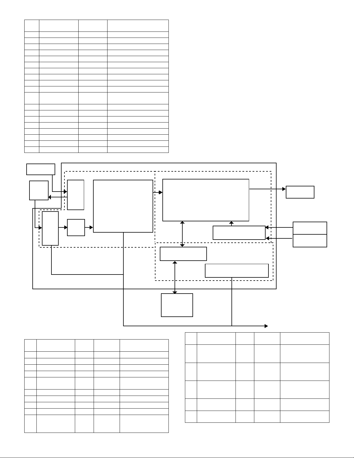
PIN
No.
Signal code
Input/
Output
Operating
110 USBIN Input IF PWB detection signal
111 Input NC
112 Input NC
113 Avss DGND
114 GND DGND
115 /SCANSP Output Scan STOP signal
116 /SCANST Output Scan START signal
117 /TRANSST Output ASIC transfer signal
118 /PRINTST Output Print Start signal
119 SPMT3 Output SPF motor signal
120 SPMT2/MIRCNT Output/
Input
SPF motor signal/mirror
counter
121 SPMT1 Output SPF motor signal
122 SPMT0 Output SPF motor signal
123 GND DGND
124 GND DGND
125 Vcc CPU3.3V
126 PSL Output Power save LED control
127 NC
128 /CS2 Output ASIC chip select
(3) Image process ASIC (HG73C119HF)
a. General
The ASIC is composed of the three major blocks: the image process
section, the print control section, and the I/F section.
Image process section:
With image data from the CCD PWB in the operation mode determined by the register setup, shading, AE process, input γ correc-
tion, area separation, filter process, resolution conversion, zoom
process, output γ correction, binary conversion (error diffusion,
dither method, simple binary conversion) are performed.
Print control section:
When copying, the image-processed data are outputted to the LSU
according to the LSU writing timing. When scanning, the image
data are made into 8bit width and outputted to the I/F section
(USB).
I/F section:
Controls the DRAM which is the image data buffer, and processes
data send/receive between the USB I/F and the IEEE1284 I/F.
The ASIC is controlled by writing the operation mode and the necessary setup values of the operation mode into the ASIC control register
before starting each operation. (For ASIC Pin configuration, refer to the
table at the end of this document.)
Scan start
CCD
PWB
Shading
ASIC
Image process section
CCD drive
Resolution conversion,
Zooming, lmage
process circuit
AE
b. ASIC (Signal table)
PIN
Signal Name IN/OUT
No.
Connected
to
Description
1 cpu_ad7 IN CPU CPU address bus
2 cpu_ad6 IN CPU CPU address bus
3 cpu_ad5 IN CPU CPU address bus
4 cpu_ad4 IN CPU CPU address bus
5 VCC(CORE/DC)
Power
3.3V
6 cpu_ad3 IN CPU CPU address bus
7 cpu_ad2 IN CPU CPU address bus
8 GND(CORE/DC) Power
9 cpu_ad1 IN CPU CPU address bus
10 sgs OUT Tr array IC SPF/RSPF gate
solenoid control signal
"H":ON
Print control section
Print data process circuit
DRAM control
I/F section
DRAM
8MB or 16MB
PIN
No.
11 srrc OUT Tr array IC SPF/RSPF resist roller
12 spus OUT Tr array IC SPF/RSPF document
13 spfs OUT Tr array IC SPF/RSPF document
14 mrps1 OUT Tr array IC SPF/RSPF motor
15 mrps2 OUT Tr array IC SPF/RSPF motor
PRINT control
ASIC control resistor
Signal Name IN/OUT
To CPU bus
Connected
to
LSU
HSYNC
VSYNC
Description
clutch control signal
"H":ON
feed solenoid control
signal "H":ON
transport solenoid
control signal "H":ON
current control signal
current control signal
AR-5012 ELECTRICAL SECTION 13 - 4
Page 75

PIN
Signal Name IN/OUT
No.
16 ope_latch OUT Tr array IC Operation circuit latch
17 op_data OUT Tr array IC Operation circuit data
18 VCC(AC) 3.3V Power
19 op_clk OUT Tr array IC Operation circuit clock
20 vfmcnt OUT Tr array IC Ventilation fan rotation
21 GND(AC) Power
22 vfm OUT Tr array IC Ventilation fan control
23 tc OUT Tr array IC Transfer charger
24 gridl OUT Tr array IC Main charger grid
25 mc OUT Tr array IC Main charger control
26 mrps3 OUT Tr array IC SPF/RSPF motor
27 mm_y3 OUT Tr array IC Carriage motor current
28 bias OUT Tr array IC DV bias control signal.
29 lden OUT Tr array IC Laser circuit control
30 pmd OUT Tr array IC Polygon motor control
31 GND(CORE/DC) Power
32 mmd OUT Tr array IC Main motor control
33 GND(CORE/DC) Power
34 VCC(CORE/DC)
3.3V
35 mpfs OUT Tr array IC Manual feed solenoid
36 cpfs2 OUT Tr array IC Second cassette
37 cpfs1 OUT Tr array IC Cassette paper feed
38 poffr (Not used)
39 rrs OUT Tr array IC Resist roller solenoid
40 pr OUT Tr array IC Power relay control
41 hl OUT Tr array IC Heater lamp control
42 TMON OUT Tr array IC (Not used)
43 TM_ OUT Buffer IC Toner motor control
44 VCC(AC) 3.3V Power
45 TM OUT Buffer IC Toner motor control
46 miron OUT Buffer IC SPF scanner select
47 GND(AC) Power
48 spfon OUT Buffer IC SPF ON signal
Power
Connected
to
Description
signal. Data take-in at
"L"
signal
signal
speed control signal.
"H": High speed, "L":
Low speed
signal. "H": Fan ON
control signal. "H":ON
control signal. "H": L
output
signal. "H": ON
current control signal
control signal
"H":ON
signal. "H": Laser
circuit ON
signal. "H": Polygon
motor ON
signal. "H": Main motor
ON
control signal. "H": ON
paper feed solenoid
control signal. "H":ON
solenoid control
signal. "H":ON
control signal. "H":ON
signal. "H":ON
signal. "H":ON
signal
signal
signal
PIN
Signal Name IN/OUT
No.
49 mircnt OUT Buffer IC SPF scanner select
50 GND(AC) Power
51 pcl_s_print (Not used)
52 fax_s_print (Not used)
53 es_s_print (Not used)
54 prareaen (Not used)
55 d_s_ATDI_B (Not used)
56 GND(CORE/DC) Power
57 VCC(CORE/
GND) 3.3V
58 pfclko (Not used)
59 RESET IN ASIC reset signal
60 GND(CORE/DC) Power
61 ATRST IN (Not used)
62 ATCK (Not used)
63 ATMS (Not used)
64 VCC(AC) 3.3V Power
65 ie1284_stb IN I/F board
66 ie1284_autofd IN I/F board
67 ie1284_slctin IN I/F board
68 ie1284_init IN I/F board
69 VCC(CORE/DC)
3.3V
70 ie1284_slct OUT I/F board
71 ie1284_pe OUT I/F board
72 GND(CORE/DC) Power
73 ie1284_busy OUT I/F board
74 ie1284_ack OUT I/F board
75 ie1284_fault OUT I/F board
76 ie1284_rev OUT I/F board
77 ie1284_parad7 IN/OUT I/F board
78 ie1284_parad6 IN/OUT I/F board
79 ie1284_parad5 IN/OUT I/F board
80 ie1284_parad4 IN/OUT I/F board
81 ie1284_parad3 IN/OUT I/F board
82 VCC(AC) 3.3V
83 ie1284_parad2 IN/OUT I/F board
84 ie1284_parad1 IN/OUT I/F board
85 GND(AC) Power
Power
Connected
to
connector
connector
connector
connector
connector
connector
connector
connector
connector
connector
connector
connector
connector
connector
connector
connector
connector
Description
signal
/STB signal
(IEEE1284
communication port)
/AUTOFD signal
(IEEE1284
communication port)
/SLCTIN signal
(IEEE1284
communication port)
/INIT signal
(IEEE1284
communication port)
SLCT signal
(IEEE1284
communication port)
PE signal (IEEE1284
communication port)
BUSY signal
(IEEE1284
communication port)
/ACK signal
(IEEE1284
communication port)
/FAULT signal
(IEEE1284
communication port)
/REV signal
(IEEE1284
communication port)
DATA bus (IEEE1284
communication port)
DATA bus (IEEE1284
communication port)
DATA bus (IEEE1284
communication port)
DATA bus (IEEE1284
communication port)
DATA bus (IEEE1284
communication port)
DATA bus (IEEE1284
communication port)
DATA bus (IEEE1284
communication port)
AR-5012 ELECTRICAL SECTION 13 - 5
Page 76

PIN
Signal Name IN/OUT
No.
86 ie1284_parad0 IN/OUT I/F board
87 suspend OUT I/F board
88 vmin IN I/F board
89 vpin IN I/F board
90 rcv IN I/F board
91 oen OUT I/F board
92 vmout OUT I/F board
93 vpout OUT I/F board
94 tm2_15m (Not used)
95 VCC(PLL) 3.3V Power
96 GND(PLL) Power
97 VCC(PLL) 3.3V Power
98 GND(PLL) Power
99 pfclk IN Clock
100 VCC(CORE/DC)
3.3V
101 GND(CORE/DC) Power
102 ram_data0 IN/OUT SDRAM SDRAM (Image
103 ram_data1 IN/OUT SDRAM SDRAM (Image
104 ram_data2 IN/OUT SDRAM SDRAM (Image
105 GND(AC) Power
106 ram_data3 IN/OUT SDRAM SDRAM (Image
107 ram_data4 IN/OUT SDRAM SDRAM (Image
108 VCC(AC) 3.3V Power
109 ram_data5 IN/OUT SDRAM SDRAM (Image
110 ram_data6 IN/OUT SDRAM SDRAM (Image
111 GND(CORE/DC) Power
112 ram_data7 IN/OUT SDRAM SDRAM (Image
113 ram_data15 IN/OUT SDRAM SDRAM (Image
114 ram_data14 IN/OUT SDRAM SDRAM (Image
115 VCC(CORE/DC)
3.3V
116 ram_data13 IN/OUT SDRAM SDRAM (Image
117 ram_data12 IN/OUT SDRAM SDRAM (Image
Power
Power
Connected
to
connector
connector
connector
connector
connector
connector
connector
connector
Description
DATA bus (IEEE1284
communication port)
SUSPEND signal
(USB communication
port)
VMIN signal (USB
communication port)
VPIN signal (USB
communication port)
RCV signal (USB
communication port)
OEN signal (USB
communication port)
VMOUT signal (USB
communication port)
VPOUT signal (USB
communication port)
process page
memory) data bus
process page
memory) data bus
process page
memory) data bus
process page
memory) data bus
process page
memory) data bus
process page
memory) data bus
process page
memory) data bus
process page
memory) data bus
process page
memory) data bus
process page
memory) data bus
process page
memory) data bus
process page
memory) data bus
PIN
Signal Name IN/OUT
No.
118 GND(CORE/DC) Power
119 ram_data11 IN/OUT SDRAM SDRAM (Image
120 ram_data10 IN/OUT SDRAM SDRAM (Image
121 VCC(CORE/DC)
3.3V
122 ram_data9 IN/OUT SDRAM SDRAM (Image
123 ram_data8 IN/OUT SDRAM SDRAM (Image
124 GND(AC) Power
125 ram_clk OUT SDRAM SDRAM (Image
126 ram_cke OUT SDRAM SDRAM (Image
127 xram_wde OUT SDRAM SDRAM (Image
128 VCC(AC) 3.3V Power
129 GND(CORE/DC) Power
130 xram_cas OUT SDRAM SDRAM (Image
131 xram_ras OUT SDRAM SDRAM (Image
132 xram_cs OUT SDRAM (Image
133 VCC(CORE/DC)
3.3V
134 ram_banks0 OUT SDRAM SDRAM (Image
135 ram_banks1 OUT SDRAM SDRAM (Image
136 GND(CORE/DC) Power
137 ram_dqm0 OUT SDRAM SDRAM (Image
138 ram_dqm1 OUT SDRAM SDRAM (Image
139 ram_mad12 OUT SDRAM SDRAM (Image
140 VCC(CORE/DC)
3.3V
141 ram_mad11 OUT SDRAM SDRAM (Image
142 ram_mad9 OUT SDRAM SDRAM (Image
143 GND(AC)
144 ram_mad8 OUT SDRAM SDRAM (Image
Power
Power
Connected
to
Description
process page
memory) data bus
process page
memory) data bus
process page
memory) data bus
process page
memory) data bus
process page
memory) CLK signal
process page
memory) CKE signal
process page
memory) WDE signal
process page
memory) CAS signal
process page
memory) RAS signal
process page
memory) CS signal
process page
memory) BANK signal
process page
memory) BANK signal
process page
memory) DQM signal
process page
memory) DQM signal
process page
memory) address bus
process page
memory) address bus
process page
memory) address bus
process page
memory) address bus
AR-5012 ELECTRICAL SECTION 13 - 6
Page 77

PIN
Signal Name IN/OUT
No.
145 ram_mad7 OUT SDRAM SDRAM (Image
146 VCC(AC)
147 ram_mad6 OUT SDRAM SDRAM (Image
148 ram_mad5 OUT SDRAM SDRAM (Image
149 GND(CORE/DC)
150 ram_mad4 OUT SDRAM SDRAM (Image
151 ram_mad10 OUT SDRAM SDRAM (Image
152 ram_mad0 OUT SDRAM SDRAM (Image
153 VCC(CORE/DC)
154 ram_mad1 OUT SDRAM SDRAM (Image
155 ram_mad2 OUT SDRAM SDRAM (Image
156 ram_mad3 OUT SDRAM SDRAM (Image
157 d_s_ATDO_B (Not used)
158 cl OUT Logic IC Copy lamp control
159 VCC(CORE/DC)
3.3V
160 afp_oeb (Not used)
161 ccd_tg OUT CCD PWB CCD control signal
162 GND(CORE/DC) Power
163 afp_vsmp OUT CCD PWB AFE control signal
164 ccdrs OUT CCD PWB CCD control signal
165 ccdcp OUT CCD PWB CCD control signal
166 VCC(AC) 3.3V Power
167 afp_bsmp OUT CCD PWB AFE control signal
168 ccd_ph2 OUT CCD PWB CCD control signal
169 afp_afesdi OUT CCD PWB AFE control signal
170 GND(AC) Power
171 ccd_ph1 OUT CCD PWB CCD control signal
172 VCC(CORE/DC)
173 afp_adcclk OUT CCD PWB AFE control signal
174 afp_afesen OUT CCD PWB AFE control signal
175 GND(CORE/DC) Power
176 afp_afesck OUT CCD PWB AFE control signal
177 mtr_at_home IN CCD PWB Carriage home
178 VCC(CORE/DC) Power
179 afp_data7 IN CCD PWB Image scan data
180 afp_data6 IN CCD PWB Image scan data
181 afp_data5 IN CCD PWB Image scan data
182 GND(CORE/DC) Power
183 afp_data4 IN CCD PWB Image scan data
184 afp_data3 IN CCD PWB Image scan data
185 VCC(AC) 3.3V Power
186 afp_data2 IN CCD PWB Image scan data
187 afp_data1 IN CCD PWB Image scan data
188 GND(AC) Power
Power
Connected
to
Description
process page
memory) address bus
process page
memory) address bus
process page
memory) address bus
process page
memory) address bus
process page
memory) address bus
process page
memory) address bus
process page
memory) address bus
process page
memory) address bus
process page
memory) address bus
signal
position signal
PIN
Signal Name IN/OUT
No.
189 afp_data0 IN CCD PWB Image scan data
190 GND(CORE/DC) Power
191 sfclk IN Clock
192 tm2_24m (Not used)
193 GND(PLL) Power
194 VCC(PLL) 3.3V Power
195 GND(PLL) Power
196 VCC(PLL) 3.3V Power
197 VCC(CORE/DC)
3.3V
198 mtr_y1 OUT Tr array IC Carriage motor current
199 mtr_phase1 OUT Motor
200 GND(CORE/DC) Power
201 mtr_i01 OUT Motor
202 mtr_i11 OUT Motor
203 mtr_i21 OUT Motor
204 mtr_phase2 OUT Motor
205 VCC(CORE/DC)
3.3V
206 mtr_i02 OUT Motor
207 mtr_i12 OUT Motor
208 mtr_i22 OUT Motor
209 mtr_y2 OUT Tr array IC Carriage motor current
210 VCC(AC) 3.3V Power
211 xsync IN LSU Horizontal sync signal
212 xld OUT LSU Laser drive signal
213 GND(AC) Power
214 xlend OUT LSU Laser APC signal
215 xcpuwr IN CPU CPU write signal
216 xcpurd IN CPU CPU read signal
217 scanstop IN CPU Scan stop signal
218 scanst IN CPU Scan start signal
219 transst IN CPU Data transfer start
220 printst IN CPU Print start signal
221 tmen IN CPU Toner motor clock
222 testpin4 (Not used)
223 VCC(CORE/DC)
3.3V
224 testpin3 (Not used)
225 tmclk IN Toner motor clock
226 GND(CORE/DC) Power
227 testpin2 (Not used)
228 testpin1 (Not used)
229 testpin0 (Not used)
230 cpudata15 IN/OUT CPU CPU data bus
231 cpudata14 IN/OUT CPU CPU data bus
232 cpudata13 IN/OUT CPU CPU data bus
233 cpudata12 IN/OUT CPU CPU data bus
234 cpudata11 IN/OUT CPU CPU data bus
Power
Power
Power
Connected
to
driver
driver
driver
driver
driver
driver
driver
driver
Description
control signal
Carriage motor control
signal
Carriage motor control
signal
Carriage motor control
signal
Carriage motor control
signal
Carriage motor control
signal
Carriage motor control
signal
Carriage motor control
signal
Carriage motor control
signal
control signal
from LSU (/SYNC)
(/VIDEO)
(/LEND)
signal
enable signal
signal
AR-5012 ELECTRICAL SECTION 13 - 7
Page 78
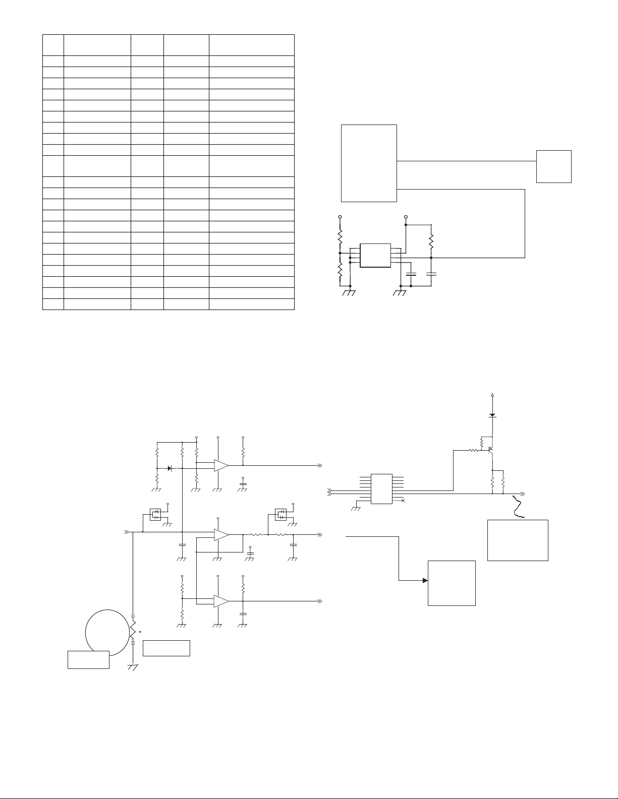
PIN
Signal Name IN/OUT
No.
Connected
to
Description
235 cpudata10 IN/OUT CPU CPU data bus
236 VCC(AC) 3.3V Power
237 cpudata9 IN/OUT CPU CPU data bus
238 cpudata8 IN/OUT CPU CPU data bus
239 GND(CORE/DC) Power
240 cpudata7 IN/OUT CPU CPU data bus
241 cpudata6 IN/OUT CPU CPU data bus
242 cpudata5 IN/OUT CPU CPU data bus
243 cpudata4 IN/OUT CPU CPU data bus
244 VCC(CORE/DC)
Power
3.3V
245 cpudata3 IN/OUT CPU CPU data bus
246 cpudata2 IN/OUT CPU CPU data bus
247 cpudata1 IN/OUT CPU CPU data bus
248 cpudata0 IN/OUT CPU CPU data bus
249 VCC(AC) 3.3V Power
250 xcpucs IN CPU CS signal
251 mem_intr (Not used)
252 GND(AC) Power
253 arb_intr OUT CPU INTR signal
254 cpusync OUT CPU CPU SYNC signal
255 cpu_ad9 IN CPU CPU address bus
256 cpu_ad8 IN CPU CPU address bus
(3) Reset circuit
This circuit detects ON/OFF of power to control start/stop of each circuit. The 3.3V voltage of the main PWB is detected by the reset IC to
generate the reset signal.
When the power voltage reaches the specified level, the circuit operations are started. Before the power voltage falls below the specified
level, the circuit operations are stopped to prevent against malfunctions.
CPU
P34
/RES
VCC3 VCC3
R114
11kF
IC104
1
NC
2
IN
3
NC
4
GND
R117
10kF
M51957BFP
Reset _OUT (ASIC Reset)
R115
10kJ
C124
0.1u
C125
22000p
VCC
OUT
8
NC
7
6
5
Cd
ASIC
(4) Heater lamp control circuit
a. Outline
The heater lamp control circuit detects the heat roller surface temperature and converts in into a voltage level. The converted voltage is
inputted to the CPU analog input pin.
12VVCC3
VCC3
R156
R155
(9-C2)
RTH_IN
R154
1kF
D101
MA700
R158
10kF
VCC3 VCC3
D102
2
3
1
DA204K
or KDS226
C197
22000p
12
1MF
R171
1.2kF
R173
10kF
7.5kF
R159
4.3kF
3
+
2
-
12V
3
+
2
-
12VVCC3
5
+
6
-
84
IC120A
NJM2903
or KIA393F
84
IC122A
LM358
or KIA358F
84
IC120B
NJM2903
or KIA393F
R157
1kJ
1
12V
C196
0.1u
D103
2
3
1
DA204K
or KDS226
R169
R170
300J
12V
R172
10kJ
C200
22000p
C199
0.1u
100J
1
5V
7
The CPU converts the inputted analog voltage into a digital signal level
and compares it with the set value of the simulation to control on/off the
heater lamp according to the level, maintaining the heat roller surface
temperature at a constant level.
SW5V
AK
D103
1SS133
GND
Q205
OUT
240J
R274
To AC circuit
(Heater lamp
Control)
240J
R280
C198
0.1u
(3-3B) HL
HT EMP
FTH
RTH
THOPEN
(5-B2)
(1-A3)
(4-A3)
IC205
I11O1
I22O2
3
I3
4
I4
5
I5
6
I6
7
I7
8
COM
TD62503F
DTA143XKA
IN
16
15
14
O3
13
O4
12
O5
11
O6
10
O7
9
NC
/HL
CPU
AN0
HLOUT (10-3A)
t
Thermistor
Heat Roller
The lower the heat roller surface temperature is, the greater the thermistor resistance is, and vise versa.
Therefore, the lower the heat roller surface temperature is, the higher
the thermistor terminal voltage is, and vise versa. The thermistor terminal voltage is inputted to the CPU analog port.
The CPU controls ON/OFF of the heater lamp by this input voltage
level.
AR-5012 ELECTRICAL SECTION 13 - 8
[High temperature protect circuit in case of CPU hung up]
For IC120 3pin (reference voltage), +3.3V is divided by the resistor.
The thermistor terminal voltage is inputted to IC120 2pin.
When, the voltage at 2pin becomes lower than the voltage at 3pin
(when the heat roller temperature is about 220 – 230°C), IC120 1pin
becomes HIGH, and the HL signal is lowered to the GND potential
through IC124, stopping generation of the heater lamp ON signal.
(IC120 1pin is normal LOW.)
Page 79
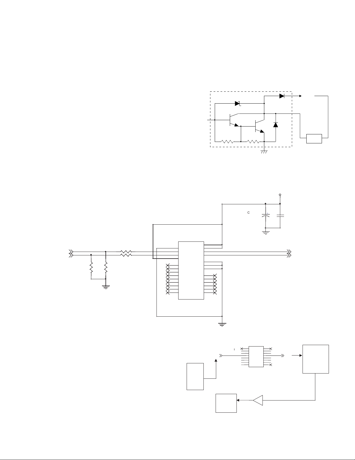
[When the heat roller surface temperature is lower than the set
level]
1) Since the thermistor terminal voltage is higher than the set level,
the HL signal from the CPU becomes HIGH.
2) The HL signal is turned to be the HLOUT signal through IC124 protect circuit, and inputted to the photo triac coupler on the power
PWB.
3) When the internal triac turns on, a pulse is applied to the gate of the
external triac. Consequently a current flow from the power source
through the heater lamp to the triac, lighting the heater lamp.
[When the heat roller surface temperature is higher than the set
level]
1) Since the thermistor terminal voltage becomes lower than the set
value, the HL signal from the CPU becomes LOW.
2) The HL turns LOW, the photo triac coupler on the power PWB turns
OFF, the external triac turns OFF, and the heater lamp turns OFF.
[In case of the thermistor open]
The voltage at IC120 6pin over the voltage at 5pin to drive the output
THOPEN at 7pin to LOW. This is passed to the CPU and the trouble
code "H2" is displayed.
(6) Toner supply motor drive circuit
The IC129 is the motor control IC, which generates the pseudo AC
waveform with the pulse signals (TM, TM-) outputted from ASIC, driving the toner supply motor.
(5) Driver circuit (Solenoid)
a. Outline
Since the load signal from the CPU or the ASIC cannot drive the load
directly, it is passed through the driver IC to drive the load.
b. Operation
The driver circuit forms a Darlington circuit with transistors. Therefore a
large drive current is obtained from a small current (ASIC output current). When the driver input voltage (base resistance input) is HIGH
(+3.3V), the transistor turns ON to flow a current in the arrow direction,
operating the load. When the driver is ON, the driver output terminal
voltage is 0V.
+24V
ASIC/CPU
OUT PUT
LOAD
LOAD
R187
(4-D3)
(4-D3)
(TM)
(TM_)
R204
47kJ
R205
47kJ
PGND
1kJ
R188
1kJ
(7) Main motor drive circuit
The main motor is driven by the MMD signal from ASIC. While the
main motor is rotating, the MMD signal is driven to HIGH and passed
through IC125 to the control circuit in the main motor to rotate the main
motor. When the main motor speed reaches the specified rpm, the
MMLD signal is turned LOW and passed through IC115 to the CPU.
24V
C212
10u/35V
1
2
3
4
5
6
7
8
IC201
I1
I2
I3
I4
I5
I6
I7
COM
TD62503F
PGND
16
O1
15
O2
14
O3
13
O4
12
O5
11
O6
10
O7
NC
IC129
19
PSAVE
20
Rin
18
Fin
21
VREF
1
NC
2
NC
3
NC
4
NC
7
NC
10
NC
11
NC
12
NC
13
NC
BA6920FP
OUT1
OUT2
RNF
GND
Vcc
FIN
NC
NC
NC
NC
NC
NC
17
16
VM
9
5
6
8
FIN
25
24
23
22
15
14
PGND
MMD MMD
C213
+
0.1u/50V
TMB_O
(9-A1)
TMA_O
(9-A1)
/MMD
9
Main Motor
Control
Circuit
( Main Motor)
ASIC
MMLD
AR-5012 ELECTRICAL SECTION 13 - 9
CPU
Page 80

(8) Mirror motor control circuit, Duplex motor control circuit
Stepping motors are employed for the mirror motor, the SPF motor,
and the duplex motor. The driver for IC127 (for mirror motor) is the
bipolar drive L6219DS, and the driver for IC128 (for SPF) is the unipolar drive IC MTD1361F. For control, the SPF outputs the drive signal
from the CPU to the IC, and the mirror outputs the drive signal to the IC
with the ASIC. They drive each motor in 1-2 phase excitement or 2phase excitement.
Each motor switches the motor current value in each magnification
ratio.
• SPF motor drive circuit
PGND
C215 OPEN
R197 1J 2W
R198 2.4kJ
R203 2.4kJ
R206 1J 2W
C232 OPEN
(4-D2)
(4-D2)
(4-D2)
(4-D2)
(SPMT2)
(SPMT0)
(SPMT3)
(SPMT1)
R195
1kJ
C218
2200p
C222
2200p
R207
1kJ
C217
47u/16V
R199
R200
620J
R201
1.2kJ
(5-C2)
(5-C2)
(5-C2)
MRPS_1
MRPS_2
MRPS_3
300J
• Mirror motor drive circuit
PGND
5V
R196
+
750J
R202
100J
PGND
C220
0.1u
PGND
C219
+
47u/16V
PGND
C211 2200p
R191 7.5kJ
R194 7.5kJ
C214 2200p
C216
OPEN
C227
OPEN
23
20
25
24
19
12
18
26
27
17
16
3
IC128
CrA
CrB
VsA
RsA
VrefA
VrefB
RsB
VsB
In /A
In A
In /B
In B
MTD1361/F
24VM
22
Vmm
1
OUT /A
4
OUT A
14
OUT /B
11
OUT B
15
PG
28
PG
PGND PGND
D112 OPEN
D113 OPEN
¢UT
D114 OPEN
D115 OPEN
SPMT_2
SPMT_0
SPMT_3
SPMT_1
(9-E1)
(9-D1)
(9-D1)
(9-E1)
(8-C3)
(8-C3)
(8-C3)
(8-C3)
OUT_AOUT_A+
OUT_B+
OUT_B-
(5-C1)
(5-C1)
(5-C1)
MMref0
MMref1
MMref2
D105 OPEN
D106 OPEN
R184
2kJ
D107 OPEN
D108 OPEN
PGND PGND
5V
R181
1kJ
R186
R185
510J
1kJ
C205
0.1u
R178
0.68J
1W
C202
820p
PGND
(2-A3)
(2-A3)
(2-A3)
R180
1.5kJ
MM_BI0
MM_BI1
MM_PH_B
C203
820p
PGND
IC127
1
OUT 1A
2
OUT 2A
3
SENSE 2
4
COMP 2
5
OUT 2B
6
GND
7
GND
8
I02
9
I12
10
PHASE 2
11
VREF 2
12
RC 2
L6219DS
PGND PGND
5V
C206
+
1u/16V
PGND
C207
0.1u
R182
30kJ
SENSE 1
COMP 1
OUT 1B
GND
GND
PHASE 1
VREF 1
RC 1
VSS
VS
I01
I11
24VM
24VM
24
23
22
21
20
19
18
17
16
15
14
13
5V
MM_AI0
MM_AI1
MM_PH_A
R183
30kJ
CP201
0603FA1.5A
CP101
ICP-N38
C209
0.1u/50V
PGND
R179
1.5kJ
C204
820p
(2-A3)
(2-A3)
(2-A3)
C210
0.1u/50V
C201
820p
R177
0.68J
1W
24V
PGND
PGND
+
C208
47u/35V
CP202
0603FA1.5A
CP102
ICP-N38
24Vdup
AR-5012 ELECTRICAL SECTION 13 - 10
Page 81
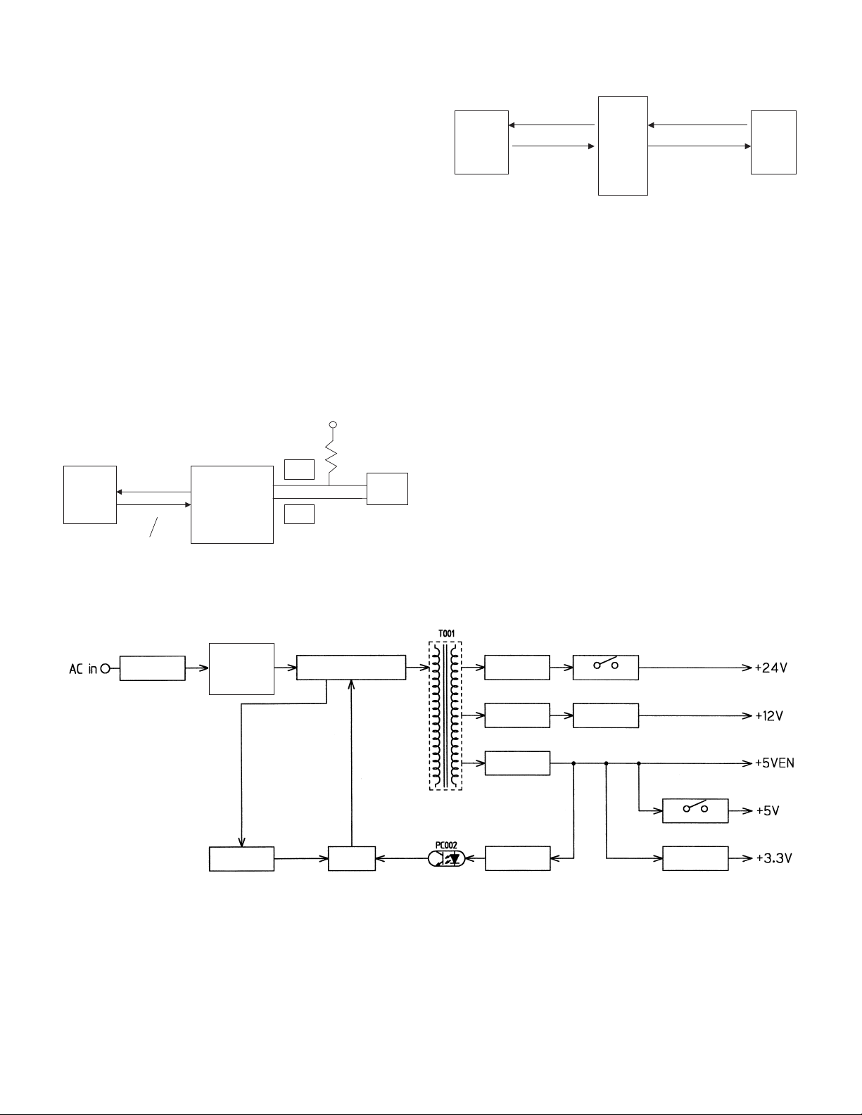
(9) Operation circuit
a. General
The operation circuit is composed of the key matrix circuit and the display matrix circuit.
b. Key matrix circuit
Select signals SELIN 1 – 3 are sent from the CPU of the MCU to the
selector in the operation circuit.
The signals detecting OFF/ON of the key are sent to the CPU as KIN 1
– 2.
c. Display circuit
The display is controlled by sending the data signal from the CPU of
the MCU, the clock signals, and the latch signals from the ASIC to the
LED driver in the operation circuit.
∗ The basic circuitry is the same as that of Puma.
(10) I/F circuit
a. General
The I/F circuit is composed of the USB driver and the IEEE1284 driver,
and performs hard interface with the ASIC (MCU PWB).
b. USB circuit
With the USB driver, the differential signals (analog) of USB are converted into digital signal, which are sent to the ASIC. In the reverse
procedure, interface between the ASIC (engine) and the host is performed.
ASIC
OE, RCV, VP, VM
Suspend, VMO
VPO
D+
USB driver
IC401
D-
USB
connector
c. IEEE1284 circuit
The IEEE1284 driver is used to perform interface between the ASIC
(engine) and the host.
ASIC
IEEE1284
driver
IC403
Centronics
connector
(11) Carriage unit
a. General
The carriage unit is provided with the CCD PWB, the inverter PWB,
and the lamps. It scans documents and transfers AD-converted image
data to the ASIC.
b. CCD PWB
The CCD on the CCD PWB employs the color image sensor uPD8861
of 5400 pixels x 3 lines, and scans documents in the main scanning
direction in the resolution of 600dpi/US letter size.
Image data scanned by the CCD are inputted to the AFE (AD9826),
and subject to CDS, amplification, and AD-conversion. Then digital
data are outputted to the MCU PWB and to the ASIC, which performs
image process of the digital data.
c. Lamp inverter PWB
The transformer is controlled by the lamp control signal from the MCU
PWB. The transformer output controls lighting of the cool cathode ray
tube.
B. DC power circuit
The DC power circuit directly rectifies the AC power and performs
switching-conversion with the DC/DC converter circuit, and rectifies
and smoothes again to generate a DC voltage.
The constant voltage control circuit is of +5VEN. +24V and +12V are of
the non-control system by winding from the +5VEN winding. As shown
in fig (1), +24V, +12V, and +5V are provided with the ON/OFF function
by external signals. +3.3V is outputted from +5VEN to the regulator IC.
Refer to the block diagram, fig (1).
Noise filter
circuit
Rush current
prevention circuit
Rectifying/
smoothing
circuit
Overcurrent
protection circuit
Inverter circuit
(Flyback converter system)
Control
circuit
fig (1) Block diagram
Rectifying/
smoothing circuit
Rectifying/
smoothing circuit
Rectifying/
smoothing circuit
Constant-voltage
detection circuit
(Semiconductor switch)
+12V regulator IC
(with ON/OFF function)
(Semiconductor switch)
+3.3V
regulator IC
AR-5012 ELECTRICAL SECTION 13 - 11
Page 82

(1) Noise filter circuit
The filter circuit is composed of L and C. It reduces common noises
and normal mode noises generated from the AC line.
The common noise means that generated in each line for GND. Its
noise component is delivered through C001, C003, and C007 to GND.
The normal noise means that overlapped in the AC line or the output
line. It is attenuated by C002, L001, C006, and L002. Refer to fig (2).
(3) Inverter and control circuit (Flyback converter system)
D103
T001
R109R111
PC002IC102
C010
Q001
fig (2) Noise filter circuit
(2) Rush current prevention circuit and rectifying/
smoothing circuit
R013
R012
R006R005
C013
R016
876
IC002
1234
5
PC002
AC
R012
fig (4) Inverter and control circuit
This circuit is one-stone separate excitation DC-DC converter called
flyback converter, as shown in fig (4).
When an electromotive voltage of IC is applied through D012, R005,
and R006 to IC002, IC002 oscillates to conduct Q001.
As a result, a voltage is applied to the primary winding of the converter
transformer (T001) and at the same time a voltage is generated in the
driving winding of IC002 to operate IC002. Then IC002 turns ON/OFF
Q001 at the frequency of about 70KHz determined by R016.
Under the ON state, the voltage in the secondary winding is reversed
to the diode D103 and no current flows through the secondary winding
of T001.
Under the OFF state, the current flowing through the primary winding is
in the same direction as the primary winding, conducting D103 and
transmitting energy to the secondary winding. Refer to fig (4).
fig (3) Rush current prevention, rectifying/smoothing circuit
Since the AC power is directly rectified, if there were not this rush current prevention resistor (TH001), an extremely large rush current
would flow due to a charging current flowing through the smoothing
capacitor C010 when turning on the power.
To prevent against this, the rush current prevention resistor TH001 is
provided between the rectifying diode D002 and the smoothing diode
C010, suppressing a rush current.
The rectifying/smoothing circuit rectifies a 50/60Hz AC voltage with the
rectifying circuit, and smoothes it with the smoothing capacitor C010.
secondary
winding
voltage
fig (5) Operation waveform of the flyback converter
AR-5012 ELECTRICAL SECTION 13 - 12
Page 83

The control circuit is subject to negative feedback from the secondary
side as shown in fig (4). A photo coupler (PC002) is employed to insulate between the primary side and the secondary side to feed back the
control signal to the primary side.
When the output voltage is increased by energy transmission from
T001, the voltage detected by R109 and R111 is compared with the
reference voltage of IC102. When it exceeds the reference voltage, the
current flowing through IC102 (that is, the photo diode current of
PC002) is increased and transmitted to the primary side. Then the
potential at the feedback pin (2 pin) of IC102 is decreased to control
Q001. Therefore, the change in the output voltage on the secondary
side is passed through IC102 and PC002 to control Q001, stabilizing
the output voltage.
(4) Overcurrent protection circuit (Primary side)
The inverter circuit of the primary side is connected with the current
detection resistor R102. When an overcurrent occurs in the secondary
side, the current flowing through the primary side inverter Q001 is
increased. The current is detected by R012, and passed through R013
to IC701 overcurrent restricting pin (3 pin) to turn OFF Q002, shutting
off all power. To resupply the power, turn off and on the power. Refer
to fig (4).
(5) Rectifying/smoothing circuit (+5V)
fig (6) Rectifying/smoothing circuit
The high frequency pulse generated by the inverter circuit is
decreased by the converter transformer, rectified by the high frequency
diode D103, and smoothed by C103 and C104.
Voltage waveform
Voltage waveform
fig (7) +5V rectifying/smoothing circuit voltage waveform
AR-5012 ELECTRICAL SECTION 13 - 13
Page 84

[14] CIRCUIT DIAGRAM
4
VCC3
1/9
E
D
5
6
VCC3
7
8
5
12
C102
*6
Spreading Range :
+/- 1.25%
VCC3
R101
OPEN
R104(*3) OPEN 0J
R103(*1) OPEN 680J
When IC101 is, mounted NOT mounted
6
7
8
5
6
7
8
21
X101
HC-49U/S
R103 *1
*2
21
R102
1
2
3
4
Xin
Vss
FS0
Xout
SSon5MODOUT6SR07VDD
IC101
8
21
12
VCC3
15pF
22pF
R107(*4) 22J OPEN
R102(*2) 0J OPEN
C103(*5)
4
19.6608MHz
C101
15pF
22pF
C102(*6)
C
B
A
MCU PWB (CPU SECTION)
1. MCU PWB
876
5
BR105
123
4
/CS0
/CS2
/CS1
876
5
BR104
123
4
D13
D12
D14
D15
4
3
2
1
BR103 10kJ
4
3
2
1
BR102 10kJ
4
3
2
1
BR101 10kJ
21
R104 *3
12
12
C103 *5
P2010/PLL701-01
R106
0J
R105
0J
0.1u
*R102,R103,C102, and C103 are temtative
876
5
BR107
10kJ
123
4
RY/BY
CCD_TG
MT_HOME
A20
876
5
BR106
10kJ
123
4
D11
D10
D9
D8
C105
100p
12
12
C104
100p
12
21
12p
C106
R107 *4
21
21
10kJ
(6-D3)
DMT3
10kJ
(6-D3)
DMT2
R276 33J
BR109
BR108
(6-D4)
DMT1
21
R277 33J21R278 100J
RD
/RD
(3-A2)(2-A2)
876
123
(FW)
CPU_SYNC
ARB_INT
876
123
D5
D7
D6
(6-D4)
(5-B2)
(5-B1)
(2-A2)
POFF
DMT0
TMEN
PMCLK
21
LWR
HWR
/LWR
/HWR
SELIN3
SELIN2
(3-A2)
(4-C3)
(4-C3)
(2-A2)
VCC3
5
4
5
4
D4
(2-A2)
TMCLK
SELIN1
(4-C3)
10kJ
10kJ
BR110
(4-D4)
(4-D4)
(3-B2)
RY/BY
(KIN1)
(KIN2)
RY/BY
CPUNRST
FAXSTS(NC)
FAXCMD(NC)
SCL
SCL
(9-B1)
C107
0.1u
1
2
VCC3
5
BR111
4
HWR
RD
CPUCLK(NC)
876
123
D3
D2
D1
VCC3
CPU3.3
CPUCLK(NC)
RESETOUT
SDA
SDA
(9-B1)
VCC3
IC102
R270
5
876
BR114
10kJ
4
123
LWR
FAXSTS(NC)
5
10kJ
4
D0
R283
8
7
6
5
21
R291 1kJ
5
6WC7
8
SCL
SDA
VCC
E01E12E23VSS
4
21
OPEN
3
876
876
10kJ
BR115
123
123
/PRINTST
SDA
SCL
FAXCMD(NC)
10kJ
21
1
2
3
4
BR112 10kJ
65
Vss
66
67
Vss
68
Vss
69
70
71
72
73
74
75
76
77
78
79
80
81
RES
82
NMI
83
STBY
84
VCC
85
XTAL
86
EXTAL
87
Vss
88
PF7/0
89
VCC
90
PF6/AS
91
PF5/RD
92
93
94
95
96
97
98
99
Vss
100
Vss
101
102
IC103
103
VCC3
24WC02 or HT24LC02
21
R271
10kJ
R108
10kJ
VCC3
3
5
10kJ
4
/SCANSP
/TRANSST
/SCANST
(9-B3)
(8-A2)
(8-C4)
(8-C1)
(8-D3)
TxD1
ONL
D_CONT
BEO
/CL_RESET
RESETOUT1
63
61
59
P31/TxD160P30/TxD0
P33/RxD162P32/RxD0
P35/SCK164P34/SCK0
P60/ /DREQ0CS4
P61/ /TEND0CS5
P62/DREQ1
P63/TEND1
P27/PO7/TIOCB5
P26/PO6/TIOCA5
P25/PO5/TIOCB4
P24/PO4/TIOCA4
P23/PO3/TIOCD3
P22/PO2/TIOCC3
P21/PO1/YICOB3
P20/PO0/TIOCA3
WDTOVF
PF4/HWR
PF3/LWR
PF1/BACK
PF0/BREQ
P50/TxD2
P51/RxD2
P52/SCK2
P53/ADTRG
AVcc
Vref
P40/AN0
P41/AN1
P42/AN2
P43/AN3
104
105
106
107
108
RTH
(SIN1)
(SIN2)
(5-E3)
(4-D3)
(4-D3)
12
21
876
5
BR117
10kJ
123
4
SPMT1
SPMT0
SPMT3
SPMT2
D12
D8
D15
D10
D7
D6
D9
D14
D13
D11
BR118
33J
876
5
123
4
BR116
33J
BR119
33J
5
876
4
123
54
53
51
49
55
Vss
PE7/D748PE6/D647PE5/D546PE4/D4
PD1/D950PD0/D8
PD4/D12
PD3/D1152PD2/D10
PD7/D1557PD6/D1456PD5/D13
HD6412320VF25(H8S/2320)
PF2/ / WAIT/BREQOLCAS
P45/AN5
P46/AN6/DA0
P47/AN7/DA1
AVss
Vss
P17/PO15/TIOCB2/TCLKD
P16/PO14/TIOCA2
P15/PO13/TIOCB1/TCLKC
P14/PO12/TIOCA1
P13/PO11/TIOCD0/TCLKB
P12/PO10/TIOCC0/TCLKA
111
112
113
114
115
116
117
118
119
120
21
21
R112 10kJ
/SCANSP
/TRANSST
/SCANST
/PRINTST
SPMT2
SPMT3
SPMT3
(USBIN)
/SCANST
/SCANSP
/PRINTST
/TRANSST
0.1u
(2-A2)
(2-A2)
(2-A2)
(2-A2)
(4-C2)
21
SPMT2/MIRCNT
(4-C2)
C108
OPEN
58
VCC
P44/AN4
109
110
(SIN3)
(4-D3)
R109
876
123
R111 10kJ
D5
D4
5
4
45
P11/PO9/TIOCB0/DACK1
121
122
SPMT1
SPMT0
SPMT1
(4-C2)
44
P10/PO8/TIOCA0/DACK0
123
SPMT0
(4-C2)
Vss
MD0
D0
D2
D1
D3
BR120
33J
876
5
123
4
40
PE3/D343PE2/D242PE1/D141PE0/D0
MD1
MD2
PG0/CAS
PG1/CS3
124
125
126
127
PSL
(8-C3)
2
VCC3
3
2
12
L101
ZJSR5101-223
1
+
C109
10u/16V
12
C115 0.1u
12
C114 0.1u
12
C113 0.1u
12
C112 0.1u
12
C111 0.1u
12
C110 0.1u
1
E
CPU3.3
(2-A2) (3-A1)
D[15..0]
(2-A1)
(4-D4)
(8-C2)
(7-E1)
(2-A1)
(2-B4)
(7-E1)
D
mt_at_home
(PSW)
CCD_TG
CPU_SYNC
ARB_INT
(SPPD)
(FW)
A20
CPU_SYNC
MT_HOME
CCD_TG
ARB_INT
(FW)
39
H8S/2320
VCC
P64/IRQ0
38
P65/IRQ1
37
Vss
36
Vss
35
P66/ /CS6 IRQ2
34
P67/ /CS7 IRQ3
33
PA7/A23/IRQ7
32
PA6/A22/IRQ6
31
PA5/A21/IRQ5
30
PA4/A20/IRQ4
29
Vss
28
PA3/A19
27
PA2/A18
26
PA1/A17
25
PA0/A16
24
PB7/A15
23
PB6/A14
22
PB5/A13
21
PB4/A12
20
Vss
19
PB3/A11
18
PB2/A10
17
PB1/A9
16
PB0/A8
15
PC7/A7
14
PC6/A6
13
PC5/A5
12
PC4/A4
11
Vss
10
PC3/A3
9
PC2/A2
8
PC1/A1
7
PC0/A0
6
VCC
5
NC
4
Vss
3
PG4/CS0
2
PG3/CS1
1
PG2/CS2
128
/CS2
/CS2
(2-A1)
/CS1
/CS1
(3-A2)
33J
BR123
33J
BR122
33J
BR121
/CS0
/CS0
(3-C2)
2
12
C123 OPEN
12
C122 OPEN
12
C121 OPEN
12
C120 OPEN
2
1
C119 OPEN
12
C118 OPEN
12
C117 OPEN
(2-A1) (3-A3)
A[19..0]
C
4
5
3
6
2
7
1
8
5
6
7
33J
8
BR125
4
5
3
6
2
7
1
8
5
6
33J
7
8
BR124
4
5
3
6
2
7
1
8
A19
A18
A17
A16
4
A15
3
A14
2
A13
1
A12
A11
A10
A9
A8
4
A7
3
A6
2
A5
1
A4
A3
A2
A1
A0
B
VCC3
VCC3
21
R115
10kJ
8
7
NC
NC1IN2NC
IC104
21
R114
11kF
(3-B2)
(9-B1) (2-D1)
CPUNRST
CPUNRST
5
6
Cd
VCC
OUT
GND
4
3
C125
22000p
12
12
C124
0.1u
M51957BFP
21
R117
10kF
VCC3
C128
12
21
R285 33J
RESETOUT1
0.1u
CPU port selection of a /ASIC_RST output
R284
10kJ
1
33J mounted on R116 and R285 are OPEN
33J mounted on R285 and R116 are OPEN
(2-D1)
PF6
P34
/ASIC_RST
C126
47p
12
21
R116 OPEN
21
R118
10kJ
21
RESETOUT
A
AR-5012 CIRCUIT DIAGRAM 14 - 1
Page 85

VCC3
876
5
8
7
876
6
5
123
4
123
4
BR145 10kJ
C162 0.1u
C161 0.1u
C160 0.1u
BR130
BR129
BR128
BR127
BR126
5
4
AFE_DB0
AFE_DB1
L110
VCC3
21
R261
12
5
OUTPUT
X102
8
12
12
3
ZJSR5101-223
1
VCC3
876
5
876
123
4
123
BR133 10kJ
BR135 10kJ
RAMDB14
RAMDB13
RAMDB12
RAMDB11
RAMDB10
RAMDB9
RAMDB8
(3-E3)
(3-E2)
(3-E2)
(3-D2)
/SDWDE
SDCKE
SDCLK
RAMDB[15..0]
BR134
33J
876
5
123
4
124
125
126
127
128
VCC(AC)
GND(AC)
RAM_CLK
RAM_CKE
GND(CORE/DC)
RAM_WDE#
129
RAM_CAS#
130
RAM_RAS#
131
RAM_CS#
132
VCC(CORE/DC)
133
RAM_BANK0
134
RAM_BANK1
135
GND(CORE/DC)
136
RAM_DQM0
137
RAM_DQM1
138
RAM_MAD12
139
VCC(CORE/DC)
140
RAM_MAD11
141
RAM_MAD9
142
GND(AC)
143
RAM_MAD8
144
RAM_MAD7
145
VCC(AC)
146
RAM_MAD6
147
RAM_MAD5
148
GND(CORE/DC)
149
RAM_MAD4
150
RAM_MAD10
151
RAM_MAD0
152
VCC(CORE/DC)
153
RAM_MAD1
154
RAM_MAD2
155
RAM_MAD3
156
TDO
157
CL
158
VCC(CORE/DC)
159
AFP_OBE
160
CCD_TG
161
GND(CORE/DC)
162
AFP_VSMP
163
CCD_PHRB
164
CCD_PHCLB
165
VCC(AC)
166
AFP_BSMP
167
CCD_PH2
168
AFP_AFESDI
169
GND(AC)
170
CCD_PH1
171
VCC(CORE/DC)
172
AFP_ADCCLK
173
AFP_AFESEN
174
GND(CORE/DC)
175
AFP_AFESCK
176
MTR_AT_HOME
177
VCC(CORE/DC)
178
AFP_DATA7
179
AFP_DATA6
180
AFP_DATA5
181
GND(CORE/DC)
182
AFP_DATA4
183
AFP_DATA3
184
VCC(AC)
185
AFP_DATA2
186
AFP_DATA1
187
GND(AC)
188
AFP_DATA0
189
GND(AC)
190
SFCLK
191
TM2_24M
192
VCC(CORE/DC)
GND(PLL)
VCC(PLL)
GND(PLL)
VCC(PLL)
197
195
196
193
4
GND
N.C.1VCC
22000p
C163
OSC-11
24MHz
194
IC106
33J
C165
12p
C164
0.1u
2
5
876
4
123
BR137 10kJ
RAMDB7
RAMDB15
RAMDB10
RAMDB9
RAMDB8
BR136
876
123
120
121
122
123
RAM_DATA9
RAM_DATA8
VCC(CORE/DC)
GND(CORE/DC)
MTR_PHASE1
MTR_Y1
201
200
199
198
MM_AI0
MM_Y1
MM_PH_A
(5-B1)
(6-C3)
5
4
RAMDB4
RAMDB5
RAMDB6
RAMDB11
33J
5
4
117
118
119
RAM_DATA11
RAM_DATA10
GND(CORE/DC)
MTR_I21
MTR_I11
MTR_I01
204
203
202
MM_AI1
MM_AI2
MM_AI0
MM_AI1
(6-C3)
(6-C3)
876
10kJ
123
BR139
RAMDB2
RAMDB3
RAMDB15
RAMDB14
RAMDB13
RAMDB12
BR138
876
5
123
4
113
114
115
116
RAM_DATA15
RAM_DATA14
RAM_DATA13
RAM_DATA12
VCC(CORE/DC)
MTR_I22
MTR_I12
MTR_I02
VCC(CORE/DC)
MTR_PHASE2
208
207
206
205
MM_BI0
MM_BI1
MM_BI2
MM_BI0
MM_BI1
MM_PH_B
(6-B3)
(6-B3)
(6-B3)
RAMDB1
33J
112
RAM_DATA7
MTR_Y2
209
MM_Y2
(5-B1)
3 3
5
4
RAMDB0
RAMDB4
RAMDB5
RAMDB6
RAMDB7
BR140
876
5
123
4
107
108
109
110
111
VCC(AC)
RAM_DATA5
RAM_DATA6
GND(CORE/DC)
GND(AC)
LD#
SYNC#
VCC(AC)
214
213
212
211
210
12
21
C166
10J
R267
(/SYNC)
(4-D4)
33J
106
RAM_DATA4
LEND#
215
/LEND
(5-B1)
47p
VCC3
3
2
1
L113
ZJSR5101-223
12
12
8
VCC
OUTPUT5GND
X103
12
C167
12p
21
R262
33J
RAMDB0
RAMDB1
RAMDB2
RAMDB3
BR141
33J
876
5
123
4
96
97
98
99
100
101
102
103
104
105
PFCLK
GND(AC)
VCC(PLL)
GND(PLL)
RAM_DATA0
RAM_DATA1
RAM_DATA2
RAM_DATA3
VCC(CORE/DC)
GND(CORE/DC)
Jaguar ASIC without PCI
SCANSP
TMEN
PRINTST#
TRANSST#
VCC(CORE/DC)
SCANST#
CPURD#
CPUWR#
TESTPIN3
TESTPIN4
217
225
221
220
219
223
218
216
224
222
TSP3
TSP4
/RD
/LWR
TMEN
/SCANSP
/SCANST
/PRINTST
/TRANSST
(1-A2)
(1-A2)
(1-B3)
(1-A2)
(1-B3)
(1-D3)
(1-A2)
1
2
5V
4
IC107
NC7ST08M5X
21
R120
100J
/VIDEO
(9-A2)
22000p
C169
C168 0.1u
1
N.C.
OSC-11
4
(8-B2)
VPOUT
VPOUT
VMOUT
21
R121
33J
876
33J
BR142
123
93
92
94
95
VPOUT
TM2_15M
VCC(PLL)
GND(PLL)
TMCLK
GND(CORE/DC)
TESTPIN1
TESTPIN2
226
229
228
227
TSP0
TSP1
TSP2
TMCLK
D[15..0]
(1-D3)
(1-D2)
C170
12
5V
2 2
13.9867MHz
PARAD0
(8-B2)
(8-B2)
(8-B2)
(8-B2)
(8-B2)
(8-B2)
VMOUT
SUSPEND
OEN
RCV
VMIN
VPIN
SUSPEND
VMIN
VPIN
RCV
876
123
5
4
87
88
89
90
91
RCV
OEN
VPIN
VMIN
VMOUT
SUSPEND
IE1284_PARAD086IE1284_PARAD184IE1284_PARAD283IE1284_PARAD3
CPU_DATA10
CPU_DATA11
CPU_DATA12
CPU_DATA13
CPU_DATA14
CPU_DATA15
TESTPIN0
235
234
233
232
231
230
D15
D13
D12
D11
D10D9D8D7D6D5D4D3D2D1D0
D14
0.1u
VCC3
VMOUT
VPOUT
PARAD1
5
4
BR143 33J
85
GND(AC)
VCC(AC)
237
236
CPU_DATA9
RCV
PARAD2
876
123
CPU_DATA8
238
R126
R125
R124
R123
R122
VCC3
E
3
2
L103
ZJSR5101-223
1
+
12
C139
47u/16V
G3.3V
12
12
12
12
12
12
12
12
12
12
C138 0.1u
C137 0.1u
C136 0.1u
C135 0.1u
C134 0.1u
C133 0.1u
C132 0.1u
C131 0.1u
C130 0.1u
C129 0.1u
1212
C149 0.1u
12
12
12
12
12
12
12
12
12
12
C148 0.1u
12
C147 0.1u
12
C146 0.1u
12
C145 0.1u
12
C144 0.1u
12
C143 0.1u
12
C142 0.1u
12
C141 0.1u
12
C140 0.1u
12
C159 0.1u
12
C158 0.1u
12
C157 0.1u
C156 0.1u
C155 0.1u
C154 0.1u
C153 0.1u
C152 0.1u
C151 0.1u
C150 0.1u
D
(3-E2)
(3-E1)
(3-D2)
(3-D2)
(3-D2)
(3-D2)
(3-D2)
(3-D2)
MAD[12..0]
DQM1
DQM0
BANK1
BANK0
/SDCS
/SDRAS
/SDCAS
33J
(9-B2)
JTG_TDO
CL
(8-C1)
R280
OPEN
C315
47p
12
21
R254
33J
VSAMP
CCD_TG
(8-E2)
(1-D2),(8-D2)
21
C317
47p
12
21
R256
33J
C318
C316
47p
12
21
R257
R255
33J
CCD_RS
CCD_CP
(8-D2)
(8-D2)
47p
21
33J
BSAMP
(8-E2)
C319
47p
21
R258
33J
12
12
CCD_PHI2
(8-D2)
C
B
C320
R259
AFE_SDI
(8-E2)
MAD12
MAD11
MAD9
MAD8
MAD7
MAD6
MAD5
MAD4
MAD10
MAD0
MAD1
MAD2
MAD3
47p
12
21
33J
CCD_PHI1
(8-D2)
33J
33J
33J
33J
12
47p
21
C321
R260
33J
ADCLK
AFE_SEN
AFE_SCK
(8-D2)
(8-D2)
(8-E2)
5
6
7
8
5
6
7
8
5
6
7
8
5
6
7
8
5
6
7
8
1
mt_at_home
(8-C2)
BR131
AFE_DB[7..0]
(8-D2)
2
876
123
33J
AFE_DB7
AFE_DB6
AFE_DB5
4
3
2
1
4
3
2
1
4
3
2
1
4
3
2
1
4
3
2
1
R119 33J
G3.3V
5
876
4
123
BR132
33J
AFE_DB4
AFE_DB3
AFE_DB2
A
MCU PWB (ASIC SECTION) 2/9
4 4
123
BR148 10kJ
BR150 10kJ
PARAD4
PARAD3
PARAD2
PARAD1
PARAD0
SUSPEND
VMIN
VPIN
(8-A2)
PARAD[7..0]
PARAD7
PARAD6
PARAD5
PARAD4
PARAD3
(8-B2)
(8-B2)
(8-B2)
(8-B2)
(8-B2)
/REV
/ACK
BUSYPE/FAULT
REV
ACK
BUSYPEFAULT
5
876
876
5
4
123
123
4
BR147 33J
BR144 33J
72
77
76
74
73
82
81
VCC(AC)
CPU_DATA7
GND(CORE/DC)
240
239
10kJ
10kJ
10kJ
10kJ
10kJ
71
75
79
IE1284_PE
IE1284_ACK#
IE1284_REV#
IE1284_BUSY
IE1284_FAULT#
GND(CORE/DC)
IE1284_PARAD678IE1284_PARAD7
IE1284_PARAD480IE1284_PARAD5
CPUCS#
VCC(AC)
CPU_DATA0
CPU_DATA1
CPU_DATA2
CPU_DATA3
VCC(CORE/DC)
CPU_DATA4
CPU_DATA5
CPU_DATA6
250
249
248
247
246
245
244
243
242
241
/CS2
(1-A2)
TSP0
TSP1
TSP2
TSP3
TSP4
R133
OPEN
21
R132
OPEN
21
R131
OPEN
21
R130
OPEN
21
R129
OPEN
2121
5
876
5
4
123
4
BR152 10kJ
FAULT
REV
PARAD7
PARAD6
PARAD5
(8-B2)
(8-B1)
(8-B1)
(8-B1)
(8-B1)
/INIT
SLCT
/SLCTIN
/AUTOFD
/STB
INIT
SLCTIN
AUTOFD
STB
SLCT
876
5
5
123
4
4
BR151 33J
BR149 33J
68
67
66
65
70
69
IE1284_INIT
IE1284_STB#
IE1284_SLCT
VCC(CORE/DC)
IE1284_SLCTIN#
IE1284_AUTOFD#
CPU_AD7
CPU_AD8
CPU_SYNC#
ARB_INTR
GND(AC)
MEM_INTR
256
255
254
253
252
251
A9
A8
ARB_INT
CPU_SYNC
(1-D2)
(1-D2)
21
21
21
21
BR153 10kJ
876
123
ACK
BUSYPESLCT
TCK
TDI
TM
TM_
HL
PR
Y3
MC
TC
R279
5
4
VCC(AC)
64
TMS
63
62
TRST
61
GND(AC)
60
RESET#
59
PFCLK0
58
VCC(CORE/DC)
57
GND(CORE/DC)
56
55
PRAREAEN
54
ES_S_PRINT
53
FAX_S_PRINT
52
PCL_S_PRINT
51
GND(CORE/DC)
50
MIRCNT
49
SPFON
48
GND(AC)
47
MIRON
46
45
VCC(AC)
44
43
TMON
42
41
40
RRS
39
POFFR
38
CPFS1
37
CPFS2
36
MPFS
35
VCC(CORE/DC)
34
GND(CORE/DC)
33
MMD
32
GND(CORE/DC)
31
PMD
30
LDEN
29
BIAS
28
27
MRPS3
26
25
GRIDL
24
23
VFM
22
GND(AC)
21
VFMCNT
20
OP_CLK
19
VCC(AC)
18
OP_DATA
17
OPE_LATCH
16
MRPS2
15
MRPS1
14
SPPS
13
SPUS
12
SRRC
11
SGS
10
CPU_AD0
9
GND(CORE/DC)
8
CPU_AD1
7
CPU_AD2
6
VCC(CORE/DC)
5
CPU_AD3
4
CPU_AD4
3
CPU_AD5
2
CPU_AD6
1
OPEN
876
5
123
4
BR154 10kJ
INIT
SLCTIN
AUTOFD
STB
VCC3
BR146 10kJ
HG73C119HF
A1
A2
A3
A4
A5
A6
A7
21
1 1
VCC3
876
123
MM_AI0
MM_AI1
(9-B2)
(9-B2)
(1-B1)
JTG_TMS
JTG_TCK
CPUNRST
A[19..0]
(1-C1)
BR155 10kJ
5
4
MM_AI2
MM_BI0
(1-B1)
(9-B2)
/ASIC_RST
JTG_TDI
ES_S_PRT
FAX_S_PRT
PCL_S_PRT
TMON
POFFR
876
123
ES_S_PRT
FAX_S_PRT
PCL_S_PRT
R127
10kJ21R128
MM_BI1
5
4
POFFR
10kJ
21
MM_BI2
TM
HL
PR
MC
TC
TM_
RRS
PMD
BIAS
VFM
SGS
R189
21
TMON
MPFS
MMD
LDEN
SPFS
SPUS
SRRC
10kJ
SPFON
MIRON
CPFS1
CPFS2
MM_Y3
MRPS3
GRIDL
MRPS2
MRPS1
MIRCNT
VFMCNT
OP_CLK
OP_DATA
OP_LATCH
(4-C2)
(4-C2)
(4-C2)
(4-C3)
(4-C3)
(5-B2)
(5-B3)
(5-B3)
(5-B3)
(5-B3)
(5-B3)
(5-B1)
(5-B1)
(5-B2)
(5-B4)
(5-B1)
(5-B2)
(5-B4)
(5-B4)
(5-B4)
(5-B3)
(5-B3)
(4-C3)
(4-C3)
(4-C3)
(5-B2)
(5-B2)
(5-A2)
(5-A2)
(5-A2)
(5-A2)
E
D
C
B
A
AR-5012 CIRCUIT DIAGRAM 14 - 2
Page 86

(2-D3)
RAMDB[15..0]
E
MAD8
MAD9
MAD4
MAD5
MAD11
MAD7
MAD12
MAD6
21
R138
OPEN
RAMDB9
RAMDB10
RAMDB11
RAMDB12
RAMDB13
RAMDB14
RAMDB15
VCC3
53
54
52
VSS
VSSQ
VCCQ
DQ02DQ14DQ25DQ37DQ48DQ510DQ611DQ7
VCC
IC110
3
VCC3
1
RAMDB0
VCC3
RAMDB1
D
C
49
VCCQ
VSSQ6VSSQ
RAMDB3
RAMDB2
RAMDB4
C174
22u/16V
12
+
R137
10kJ
RAMDB8
44
41
43
46
VSS
DQ842DQ9
DQ1045DQ1147DQ1248DQ1350DQ1451DQ15
VSSQ
VCCQ
VCC14BA1
VCCQ
9
13
12
15
RAMDB7
RAMDB5
RAMDB6
D15
A17
21
47
48
44
45
46
A16
GND
BYTE
(2-D4)
DQM1
39
UDQM
LDQM
WE
16
DQM0
/SDWDE
(2-D3)
(2-D4)
D14D9D13
(2-D3)
SDCLK
37
38NC40NC36
CLK
CAS17RAS18CS
/SDCAS
(2-D4)
D6
(2-D3)
SDCKE
CLKE
19
/SDRAS
(2-D4)
D5
35
20
/SDCS
(2-D4)
D12
34
A11
21
BANK0
(2-D4)
D4
BANK1
(2-D4)
MAD10
37
A023A124A225A3
A1022BA0
MAD0
D11D7D3
VCC
MAD1
MAD2
D10
DQ1034DQ1136DQ1239DQ1341DQ1443DQ15
A429A530A631A732A833A9
26
MAD3
D2
28
VSS
VCC
27
D1
D8
32
DQ830DQ9
SDRAM (16bit x 4bank)
D0
(1-A2)
/CS0
RDZ
A1
28CE26
25
27
A0
OE
DQ029DQ131DQ233DQ335DQ438DQ540DQ642DQ7
GND
VCC3
C327
12
C176
12
C183
0.1u
0.1u
12
C182
12
C181
12
C180
12
C179
12
C178
12
C177
12
OPEN
0.1u
0.1u
0.1u
0.1u
0.1u
0.1u
(2-D4)
MAD[12..0]
Vendor/Type
Model
SDRAM
HY57V641620HGT-P(Hyndai) MT48LC4M16A2TG-75(Micron)
K4S641632F-TC75(Samsung)
W986416DH-7(Winbond)
HY57V281620AT(Hyndai) K4S281632D-TC75(Samsung)
W981216BH-75(Winbond)
64Mb(1Mx16bitx4bank)
12/13/14 CPM
15CPM 128Mb(2Mx16bitx4bank) MT48LC8M16A2TG-75(Micron)
E
D
C
WE
A88A97A106A115A124A133A142A15
NC9NC10NC
VPP
IC111
1
21
R287 0J
VCC3
B
A
MCU PWB (MEMORY SECTION) 3/9
4 4
A[19..0]
(1-C1)
3 3
21
R286 10kJ
A16
A15
A14
D8
D9
13
14
I/O0
A0
IC112
12
11
A0
A12
A11
A13
D12
D11
D10
15
17
18
I/O1
I/O2
I/O3
I/O4
A1
A2
A3
A4
9
8
10
A2
A4
A3
RY/BY
13
11RP12WP14
15
RY/BY
HWRZ
CPUNRST
(1-D3)
(1-B1)
R139
OPEN
A10
A9
VCC3
R269
D14
D15
D13
21
30
19
20
21
I/O5
I/O6
I/O7
CS2
A75A827A926A1023A1125A124A1328A143CS1
A5
A6
7
6
A8
A13
A12
A11
A10
A9A6A7
A5
A17
18
17
16
21
A5A4A2
A7A1A6A8A19
A18
10kJ
32
VDD
A1531A162NC
22OE24WE29
A14
A15
A16
CS1Z
/CS1
(1-A2)
C173
12
RDZ
/RD
(1-B3)
A3
0.1u
HWRZ
/HWR
(1-B3)
2 2
A124A223A322A421A520A619A7
16
GND
1
LH28F400BVE
C326
12
OPEN
OPEN
A1
A17
W24L010A
C325
OPEN
12
12
C324
OPEN
OPEN
21
R289
21
R288
D[15..0]
(1-D2)
B
A
1 1
AR-5012 CIRCUIT DIAGRAM 14 - 3
Page 87

E
(1-D3)
(1-D3)
(1-D2)
(1-A3)
(1-A3)
(1-A3)
(2-A2)
(KIN1)
(KIN2)
(FW)
(SIN1)
(SIN2)
(SIN3)
(USBIN)
876
5
123
4
876
D
123
BR156 10J
VCC3
20
1Y1181Y2161Y3141Y4122Y192Y272Y352Y4
VCC
IC113
1A121A241A361A482A1112A2132A3152A4
12
VCC3
R141
10kJ
1212
5V
R140
10kJ
BR157 10J
5
4
C184
0.1u
12
3
74LCX244
1G12G
GND
17
19
10
R266
10kJ
5V
IC116
(8-D3)
(8-D3)
(8-D3)
(4-A3)
(4-A3)
(8-D3)
(SELIN1)
(SELIN2)
(SELIN3)
(OP_CLK)
20
1Y1181Y2161Y3141Y4122Y192Y272Y352Y4
VCC
1A121A241A361A482A1112A2132A3152A4
(8-D3)
(OP_DATA)
(8-D3)
(OP_LATCH)
(6-D2)
(TM)
3
17
(6-D2)
(TM_)
12
1G12G
19
R146
R147
10
10kJ
10kJ
GND
C192 100p
21
C191 100p
21
C190 100p
21
C189 0.1u
74VHCT244
21
VCC3
20
1Y1181Y2161Y3141Y4122Y192Y272Y352Y4
VCC
1A121A241A361A482A1112A2132A3152A4
IC118
BR158
10J
(6-B1)
(SPMT0)
876
123
(6-B1)
(6-B1)
(6-B1)
(SPMT1)
(SPMT2)
(SPMT3)
5
4
3
17
1
2
3
4
12
1G12G
19
10
BR159
C195
GND
10kJ
0.1u
74LCX244
8
7
6
5
E
D
FW
SIN1
SIN2
SIN3
KIN1
KIN2
/SYNC (/SYNC)
USBIN
TM
(8-C4)
(8-C4)
(8-A3)
(9-A2)
(4-B3)
(4-B3)
(4-B2)
SELIN1
SELIN2
(1-B3)
(1-B3) (4-A3)
SELIN3
OP_CLK
(2-B1)
(1-B3)
OP_DATA
(2-B1)
OP_LATCH
(2-B1)
(2-C1)
TM_
(2-C1)
C
(4-C4)
(4-C4)
SIN1
C186
33p
21
10J
C185
0.1u
21
6Y5
8
W
GND
G
9
7
5V
74HC151
5V
16
VCC
D04D13D22D31D415D514D613D712A11B10C
IC114
21
R144
B
(4-C4)
SIN2
21
R145
10J
6Y5
16
W
VCC
D04D13D22D31D415D514D613D712A11B10C
IC115
C188
C187
33p
21
0.1u
21
8
9
7
GND
G
5V
5V
74HC151
SIN3
R148
10kJ
21
21
R149
10J
6Y5
16
W
VCC
D04D13D22D31D415D514D613D712A11B10C
IC117
C194
C193
33p
21
0.1u
21
8
GND
G
7
9
74HC151
For SPF/DSPF Model Only
MIRCNT
(2-C1)
SPMT0
SPMT1
SPMT3
SPMT2/MIRCNT
(1-A2)
(1-A2)
(1-A2)
(1-A2)
MIRON
(2-C1)
SPFON
(2-C1)
C
B
21
5V
R263
10kJ
DVS1
(POD)
(TCS)
(MFD)
(PPD1)
(CED1)
(DRST)
(SELIN1)
(SELIN2)
(SELIN3)
(7-E2)
(7-E4)
(7-E3)
(7-E1)
(7-E3)
(PMRDY)
(7-E4)
(7-E3)
(7-E1)
(4-D3)
(4-D3)
(4-D3)
A
(PPD2)
(PPD3)
(7-E2)
(7-E4)
(CED2)
THOPEN
(7-E1)
(5-E2)
DSWS
(7-C4)
(MMLD)
GDIIN
(7-E3)
(8-B1)
(SPID)
(SDSW)
(7-E4)
(7-E4)
(SB4D)
(SDOD)
(9-D4)
(7-E4)
A
MCU PWB (DRIVER SECTION 1) 4/9
4 4
3 3
AR-5012 CIRCUIT DIAGRAM 14 - 4
2 2
1 1
Page 88

R172
10kJ
1
R171
1.2kF
(4-A3)
THOPEN
C200
1
2
7
IC120B
NJM2903
or KIA393F
4
8
+
-
5
6
1
2 12
R173
10kF
22000p
2
E
7
LM358
IC122B
or KIA358F
84
+
-
12V
5
6
(5-B2)
FTH
E
D103
R157
VCC3
12VVCC3
1kJ
1
R156
7.5kF
1
1
R155
1MF
1
R154
1kF
8
2
IC120A
3
2
2
2
C196
0.1u
12
12V
1
NJM2903
or KIA393F
4
+
-
2
R159
4.3kF
1
2
D101
MA700
1 2
1
R158
VCC3 VCC3
2
10kF
D102
(1-A3)
RTH
C198
0.1u
12
1
2
R170
100J
DA204K
3
or KDS226
21 21
C199
R169
IC122A
84
12V
1
2
DA204K
3
or KDS226
0.1u
300J
12
12V
1
LM358
or KIA358F
+
-
3
2
1
C197
5V
12VVCC3
2
22000p
D
RTH_IN
(9-C2)
(9-A2)
/LDEN
LDEN
(2-C1)
10
HL
(2-C1)
1
FTH
(5-E3)
R175
R174
9
NC
8
240J
2
2 1
240J
TD62503
or KID65503F
(8-B3)
HLOUT
(9-A3)
or KTA1505S
VFMOUT
Q101
2SA1036
21
R161
47kJ
2
R166
4.7kJ
1/4W
1
(8-A3)
(9-A3)
(9-B3)
(9-D3)
(9-C1)
24V 24V
/CPFS1
/CPFS2
/MPFS
1C162C153C144C135C126C117C
1B12B23B34B45B56B67B7E
IC121
21
2121212121
R160 1.5kJ
R162 1.5kJ
R163 1.5kJ
CPFS1
CPFS2
(2-C1)
(2-C1)
R164 1.5kJ
MPFS
(2-C1)
(9-C2)
/RRS
RRS
(2-C1)
R165 1.5kJ
VFM
(2-C1)
/PR
/VFMCNT
10
21
R167 1.5kJ
R168 1.5kJ
PR
VFMCNT
(2-C1)
(2-B1)
9
COM
8
TD62001AF
or KID65001AF
PGND
(8-A4)
(8-A4)
(8-B4)
24V
IC119
(8-B4)
/MC
/BIAS
/TC
/GRIDL
1C162C153C144C135C126C117C
1B12B23B34B45B56B67B7E
21
212121
R150 1.5kJ
R151 1.5kJ
R152 1.5kJ
R153 1.5kJ
TC
MC
BIAS
GRIDL
(2-C1)
(2-C1)
(2-C1)
(2-C1)
10
9
COM
8
TD62001AF
or KID65001AF
PGND
C
INT5V
1
D104
1SS133
or KRA119S
3
Q102
DTA143XKA
2
1
2
(9-A2)
(6-A1)
(6-A1)
(6-A1)
PMCLK_A
MRPS_1
MRPS_2
1C162C153C144C135C126C117C
1B12B23B34B45B56B67B7G
IC124
MRPS2
MRPS3 MRPS_3
MRPS1
PMCLK
(2-C1)
(2-B1)
(2-B1)
(1-D3)
5V
R176
240J
(9-A4)
(6-A3)
(6-A3)
MMref1
/MMD
MMref0
1C162C153C144C135C126C117C
1B12B23B34B45B56B67B7G
IC125
MMD
MM_Y2
MM_Y1
(2-C1)
(2-A2)
(2-A3)
(9-A2)
SHOLD
3
2 1
(8-B4)
(6-A3)
MMref2
POFF /POFF
MM_Y3
(2-C1)
(1-D3)
2
(9-A2)
/PMD
10
PMD
(2-C1)
9
8
/LEND
(2-A2)
Q103
NC
or KRC106S
DTC143ZKA
1
TD62503
or KID65503F
B
D
C
B
(9-E1)
(9-E1)
(9-E1)
(9-E1)
/SGS
/SPUS
/SRRC
/SPFS
24V
16
SPUS
(2-B1)
SGS
(2-B1)
SRRC
(2-B1)
COM1COM
17
8
GND
18I414NC15
TD62064AF
PGND
For SPF/DSPF Model Only
2 2
A
1 1
O12O27O39O4
I13NC4NC5I26NC10I311NC12NC13GND
IC123
A
MCU PWB (DRIVER SECTION 2) 5/9
4 4
3 3
SPFS
(2-B1)
AR-5012 CIRCUIT DIAGRAM 14 - 5
Page 89

(9-A1)
(9-A1)
6/9
C213
0.1u/50V
1
E
(9-B3)
(9-B3)
(9-B3)
(9-B3)
24Vdup
/DMT_1
/DMT_2
/DMT_3
D109
MITJ22B
8
16
O12O27O39O4
IC126
I13NC4NC5I26NC10I311NC12NC13GND
COM1COM
17
18I414NC15
GND
TD62064AF
PGND
For DSPF Model Only
D
DMT1
DMT2
DMT3
DMT0 /DMT_0
(1-D3)
(1-D3)
(1-D3)
(1-D3)
24Vdup
C
CP202
0603FA1.5A
CP102
ICP-N38
1 2
C208
47u/35V
0603FA1.5A
1 2 1 2
C206
1u/16V
+
C207
0.1u
PGND
24V
CP101
ICP-N38
1 2
PGND
24VM
+
12
1
C210
1
C209
2
0.1u/50V
2
0.1u/50V
PGND
C211 2200p
1 2
0.68J
1W
1
R179
1.5kJ
5V
OUT 1A
IC127
1
R180
1.5kJ
1
0.68J
1W
PGND
1 2
C201
820p
(2-A3)
(2-A3)
2
(2-A3)
MM_PH_A
MM_AI0
MM_AI1
14
15
16
17
19
20
21
22
23VS24
I11
I01
GND18GND
VREF 1
OUT 1B
COMP 1
PHASE 1
SENSE 1
OUT 2A2SENSE 23COMP 24OUT 2B5GND6GND7I028I129PHASE 210VREF 211RC 2
MM_BI0
MM_BI1
2
MM_PH_B
(2-A3)
(2-A3)
(2-A3)
C202
820p
1 2
5V
PGND
1 2
PGND
D108 OPEN
1 2
D107 OPEN
1 2
D106 OPEN
1 2
D105 OPEN
C204
820p
2
1
PGND
1
2
R183
30kJ
13
VSS
RC 1
L6219DS
12
R182
30kJ
2
1
1
2
C203
820p
2
1
R181
1kJ
CP201
12
5V
PGND PGND
12
PGND
2
1
C205
0.1u
2
1
R186
510J
2
1
R185
1kJ
2
1
R184
2kJ
MMref0
MMref1
MMref2
(5-C1)
(5-C1)
(5-C1)
21
R177
24VM
B
21
R178
OUT_A-
OUT_B-
OUT_A+
A
(8-C3)
(8-C3)
OUT_B+
(8-C3)
(8-C3)
24V
+
12
C212
10u/35V
21
21
1 2
C214 2200p
R191 7.5kJ
R194 7.5kJ
C215 OPEN
PGND
1 2
C216
1 2
R195
1
5V
2
24VM
PGND
IC129
IC128
OPEN
C218
1kJ
2
12
21
R197 1J 2W
R196
750J
2
1
+
12
C217
47u/16V
TMB_O
TMA_O
6
16
25
FIN
8
5
17
VM
FIN
Vcc
RNF
GND
OUT19OUT2
Rin20Fin
VREF
PSAVE19NC1NC2NC3NC4NC7NC10NC11NC12NC
18
21
21
21
R188
1kJ
R187
1kJ
1
2
R205
47kJ
2
1
R204
47kJ
(TM)
(TM_)
(4-D3)
(4-D3)
(9-D1)
(9-D1)
(9-E1)
(9-E1)
SPMT_2
SPMT_0
SPMT_3
SPMT_1
2
2
2
2
22
1
14
4
11
Vmm
OUT A
OUT B
OUT /A
OUT /B
CrA23CrB20VsA25RsA3VrefA24VrefB19RsB12VsB18In /A26In A27In /B17In B
2200p
C222
2200p
2
1
21
21
21
R198 2.4kJ
R203 2.4kJ
C219
47u/16V
+
1
2
12
C220
0.1u
2
1
R202
100J
1
2
PGND
R201
1.2kJ
2 1
R200
620J
2 1
R199
300J
PG15PG
28
16
1
PGND
C227
1
R207
R206 1J 2W
PGND
NC14NC15NC22NC23NC24NC
13
PGND
1
D115 OPEN
1
D114 OPEN
1
D113 OPEN
1
D112 OPEN
MTD1361/F
OPEN
2
1kJ
2
1 2
BA6920FP
C232 OPEN
PGND
PGND
PGND
(SPMT2)
(SPMT0)
(4-D2)
(4-D2)
PGND
(SPMT3)
(SPMT1)
(4-D2)
(4-D2)
E
D
C
For SPF/DSPF Model Only
B
A
MCU PWB (DRIVER SECTION 3)
4 4
3 3
AR-5012 CIRCUIT DIAGRAM 14 - 6
MRPS_1
MRPS_2
MRPS_3
(5-C2)
(5-C2)
(5-C2)
2 2
1 1
Page 90
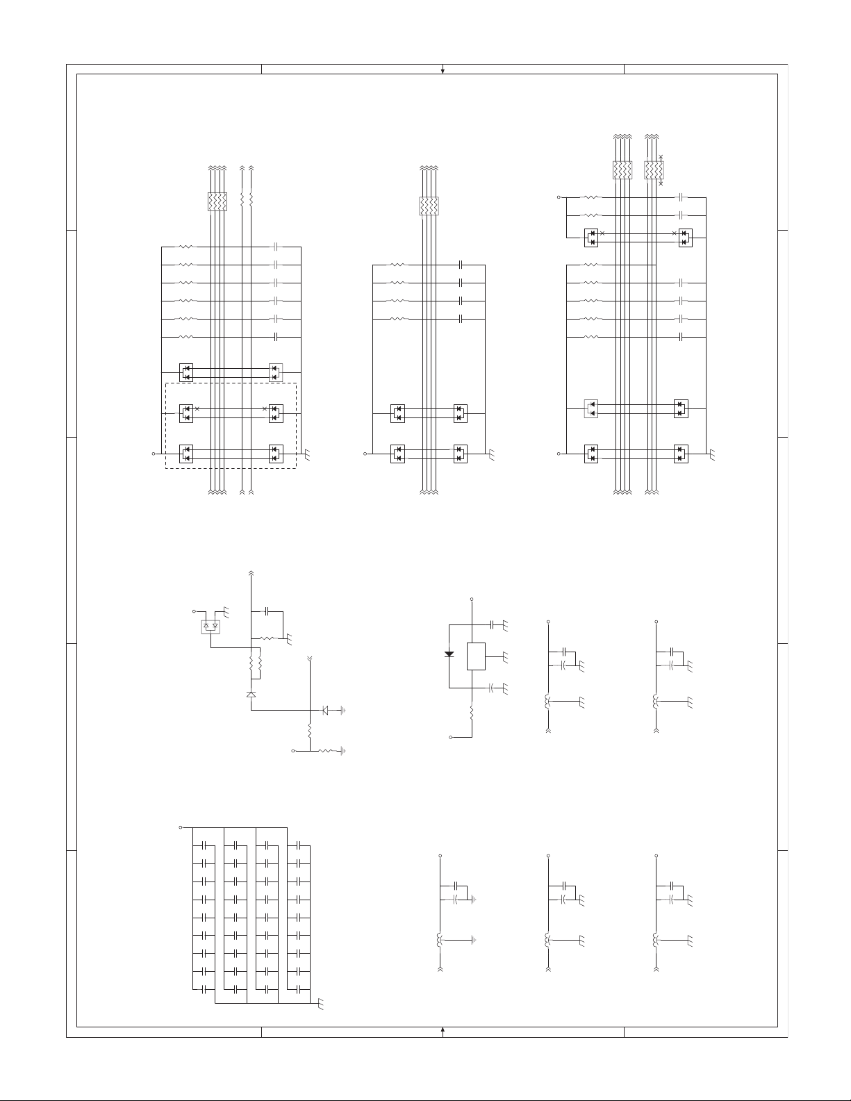
7/9
(4-A3)
(4-A3)
(4-A3)
(4-A3)
(4-A3)
(1-D2)
(1-D2)
(PPD1)
(PPD2)
(PSW)
(CED1)
(DRST)
876
123
(CED2)
5
876
5
BR163 1kJ
4
123
4
C295
1000p
1221
C292
1000p
1221
1
3
2
D134
DAP202U
or KDS120
C294
1000p
1221
C293
1000p
1221
C291
1000p
1221
C290
1000p
12 2 1
D135
DAP202U
or KDS120or KDS120
1
3
2
D133
DAP202U
1
3
2
E
D
D118
D117
D116
5V
R213
R212
R211
R210
R209
R208
DAN202U
or KDS121
3
DAN202U
3
DAN202U
or KDS121 or KDS121
3
BR160
10kJ
21
10kJ
21
39kJ
10kJ
10kJ
10kJ
2
1
2
1
2
1
(4-A2)
(SDSW)
876
123
(4-A2)
(SPID)
(4-A2)
(SB4D)
5
4
(4-A3)
(PPD3)
(4-A3)
(4-A3)
(POD)
(PMRDY)
21
21
1kJ
R214 1kJ
R216 1kJ
C266
1000p
12
C265
1000p
12
C264
1000p
1221
C263
1000p
1221
C262
1000p
1221
C261
1000p
12 2 1
D123
DAP202U
1
3
2
D122
DAP202U
1
3
2
D121
DAP202U
or KDS120 or KDS120 or KDS120
1
3
2
D126
D125
5V
R224
10kJ
2112
R223
39kJ
2112
R222
10kJ
2112
R221
10kJ
2 1
DAN202U
2
3
1
DAN202U
or KDS121 or KDS121
2
3
1
876
BR161
123
(4-A3)
DVS1
(4-A3)
(TCS)
(4-A3)
(MFD)
5
4
(4-A3)
(MMLD)
BR162 1kJ
R232
3.3kJ
VCC35V
R228
D131
DAN202U
D132
D130
3
R231
or KDS121
R230
R229
R227
R226
DAN202U
3
DAN202U
or KDS121 or KDS121
3
10kJ
7.5kJ
7.5kJ
7.5kJ
39kJ
39kJ
2
1
2
1
2
1
1kJ
C281
1000p
C280
1000p
C279
1000p
C278
1000p
12
D129
DAP202U
1
3
2
D128
DAP202U
or KDS120 or KDS120
1
3
2
E
D
POD
SPID
SB4D
PPD3
SDSW
For SPF/DSPF Model Only
(9-D1)
(9-E1)
(9-E1)
(9-D3)
(9-C2)
PMRDY
(9-A2)
C
(4-A3)
DSWS
C260
0.1u
2
DA204K
or KDS226
C250
12
C249
12
C248
12
C247
12
C246
12
C245
12
C244
12
C243
12
C242
12
R215
D120
20kJ
1SS133
OPEN
OPEN
OPEN
OPEN
OPEN
OPEN
OPEN
OPEN
OPEN
1
R218
2.7kJ
21
21
R217
1 2
C259
12
C258
12
C257
12
C256
12
C255
12
C254
12
C253
12
C252
12
C251
12
20kJ
OPEN
OPEN
OPEN
OPEN
OPEN
OPEN
OPEN
OPEN
OPEN
(9-A3)
2 1
24V1(DSWS)
D124
1SS133
1
2
21
R219
0.22J 2W
1
OPEN
OPEN
OPEN
OPEN
OPEN
OPEN
OPEN
OPEN
OPEN
R220
2
1kJ
2W
INT24V
C275
12
C274
12
C273
12
C272
12
C271
12
C270
12
C269
12
C268
12
C267
12
5V
1
2
D119
3
B
VCC3
C241
OPEN
12
C240
OPEN
12
C239
OPEN
12
C238
OPEN
12
C237
OPEN
12
C236
OPEN
12
C235
OPEN
A
12
C234
12
C233
12
OPEN
OPEN
MCU PWB (NOISE FILTER/PULL-UP SECTION)
4 4
PGNDPGND
3 3
TCS
MFD
DVSEL
(9-C4)
(9-C4)
(9-C1)
L123
ZJSR5101-223
MMLD
(9-A4)
D127
3
1
1SS133
24V
24VIN
(8-B4)
12
INT24V
12
1
C277
+
C276
2
IC130
R225
68J 2W
0.1u/50V
2
47u/35V
3
1
21
INT5V
OUT
IN
1
GND
12
PGND
PGND
C283
KIA7805
2
+
C282
0.1u
2
47u/35V
L126
ZJSR5101-223
L124
ZJSR5101-223
2 2
VCC3
3
1
3.3VIN
(8-B4)
12V
3
1
12VIN
(8-A4)
PSW
PPD1
PPD2
CED1
CED2
DRST
SPPD (SPPD)
(9-C2)
(9-C3)
(9-D1)
(9-D3)
(9-B4)
(8-D4)
(8-D4)
C
EN5V
C323
3
L127
ZJSR5101-223
1
5VEN
(8-B4)
5V
3
L125
ZJSR5101-223
1
5VIN
(8-A4)
0.1u
2
1
+
2
1
C322
22u/16V
2
B
C288
0.1u
2
1
+
1
2
C286
22u/16V
2
A
C289
0.1u
2
1
+
2
1
C287
22u/16V
2
C285
0.1u
2
1
+
2
1
C284
47u/25V
2
1 1
AR-5012 CIRCUIT DIAGRAM 14 - 7
Page 91
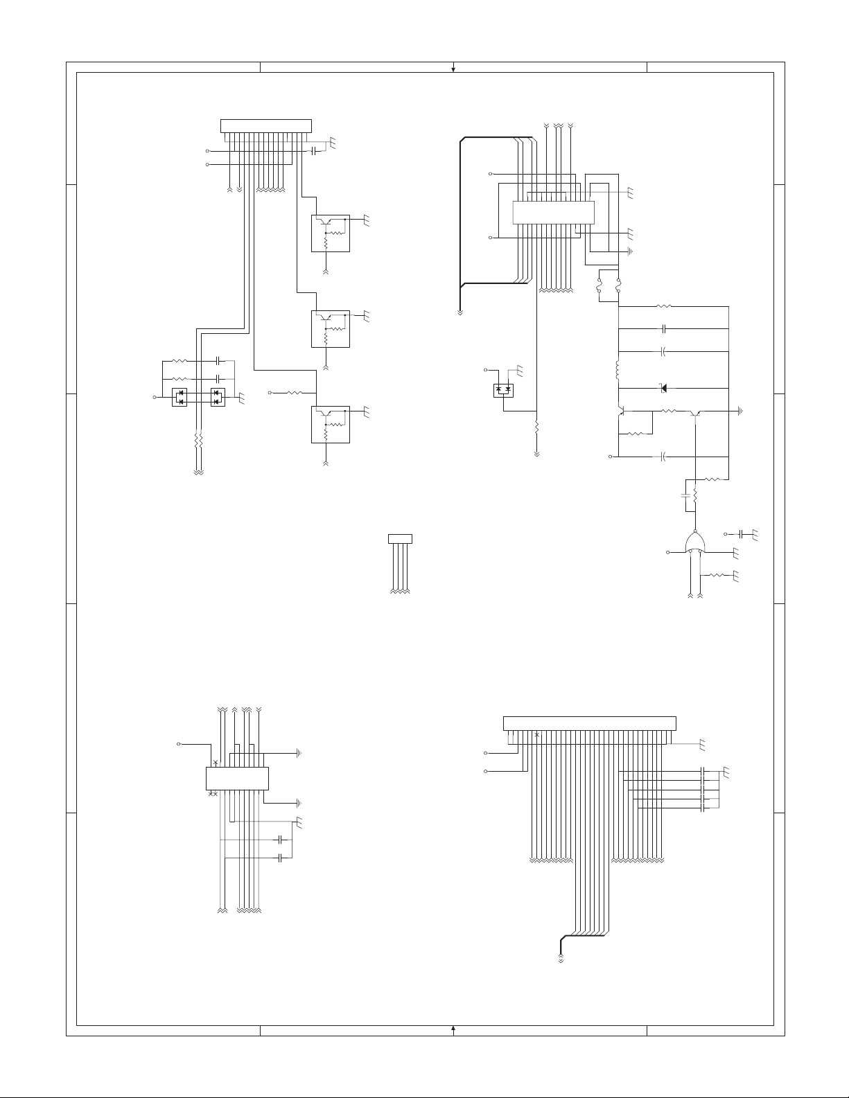
(2-B4)
(2-B4)
(2-B4)
(2-B4)
8/9
E
5V
EN5V
CN102
18
PSW
DRST
(OP_CLK)
(OP_LATCH)
(7-C1)
(7-C1)
(4-D3)
(4-D3)
(SELIN1)
(SELIN2)
(SELIN3)
(OP_DATA)
(4-D3)
(4-D3)
(4-D3)
(4-D3)
1122334455667788991010111112121313141415151616171718
12
C298
3
Q107
18FE-BT-VK-N
1000p
2
1
DTC143ZKA
EN5V
12V
To Scanner unit
D
(1-A2)
To Operational PWB
3
R281
4.7kJ
Q106
2 1
3
Q110
C297
R234
10kJ
R233
10kJ
3
5V
D136
DAN202U
or KDS121
C
1000p
1
2
2 1
C296
1000p
12
2 1
2
1
21
R235 1kJ
21
R236 1kJ
KIN2
(4-C4)
KIN1
(4-C4)
1
2
D137
DAP202U
or KDS120
5V
3
2
2
PSL ONL
(1-A2)(1-D3)
BEO
1
DTC143ZKA
or KRC106S or KRC106S
1
DTC143ZKA
or KRC106S
CN103
1122334
4
B4B-PH-K-R
AFE_DB[7..0]
(2-B3)
VCC3
D138
2
3
1
CN105
AFE_DB3
AFE_DB1
27
29
31
27
29
31
28
30
32
28
30
32
AFE_DB0
AFE_DB4
AFE_DB2
DA204K
or KDS226
R237
AFE_DB5
AFE_DB7
21
23
25
21
23
25
24
26
22
24
26
AFE_DB6
21
1kJ
mt_at_home
(2-B4)
(1-D2)
AFE_SEN
17
19
17
19
18
20
22
18
20
ADCLK
AFE_SCK
CCD_PHI1
(2-B4)
(2-B4)
(2-B4)
AFE_SDI
BSAMP
11
13
15
11
13
15
12
14
16
12
14
16
CCD_CP
CCD_RS
CCD_PHI2
(2-B4)
(2-B4)
(2-B4)
VSAMP
7
9
7
9
8
10
8
10
CCD_TG
(2-B4)
5
5
6
6
VCL
VCL
1
3
1
3
2
4
2
4
CP203
0603FA1.5A
1 2
FF4-32-S15D5Q108
CP103
L129
2SA1020
24V
ICP-N38
1 2
220uH
TWKA-221K
or KTA1281
R238
PGND
10kJ
R275
15kJ
1
2
C301
0.1u/50V
12
C300
47u/35V
+
2
1
D139
11EQS06
1
2
2 1
R239
470J
Q109
2 1
+
1
C299
47u/35V
VCC3
2SC1815
or KTC3198
2
56kJ
2 1
21
1 2
R240
15kJ R241
C302 33p
IC131
4
1
2
VCC3
NC7S08M5X
R290
10kJ
2 1
C328
12
E
D
PGND
C
0.1u
(5-C4)
(5-C4)
(5-C1)
(5-D2)
(7-A2)
(7-B1)
/TC
/POFF
HLOUT
3.3VIN
24VIN
B
INT24V
/MC
8
2244668
101012121414161618182020222224
3355779911111313151517171919212123
1
CN101
1
24
B24B-PHDSS-BC334
23
To Power unit
12
0.1u/50V
12
C335
0.1u/50V
A
/BIAS
(5-C4)
/GRIDL
(5-C4)
5VEN
(8-D3)(8-B2)
5VIN
(7-A1)
12VIN
(7-A2)
FW
(4-C4)
/PR
(5-C3)
MCU PWB (CONNECTOR SECTION 1)
4 4
PGND PGND
To Mirror motor
OUT_A+
OUT_B+
(6-A4)
(6-A4)
OUT_A-
OUT_B-
(6-A4)
(6-A4)
3 3
112233445566778899101011111212131314141515161617171818191920202121222223232424252526262727282829293030313132323333343435
CN104
VCC3
EN5V
OEN
RCV
VPIN
VMIN
USBIN
VPOUT
VMOUT
D_CONT
To Interface PWB
(1-D3)
(2-D2)
(2-D2)
(2-D2)
(2-D2)
(2-D2)
PARAD[7..0]
(2-E1)
SUSPEND
(2-D2)
(2-D2)
PARAD0
PARAD1
PARAD2
PARAD3
PARAD4
2 2
PARAD5
PARAD6
/REV
(2-D2)
PARAD7
/ACK
/FAULT
(2-D2)
(2-D1)
BUSY
(2-D1)
PE
(2-D1)
SLCT
(2-D1)
/INIT
(2-D1)
/SLCTIN
/AUTOFD
(2-D1)
(2-D1)
/STB
(2-D1)
GDIIN
(4-A3)
35
CL
/CL_RESET
(1-D3)
(2-B4)
35FE-BT-VK-N
12
12
12
12
12
B
C333 OPEN
C332 OPEN
C331 OPEN
C330 OPEN
C329 OPEN
A
1 1
AR-5012 CIRCUIT DIAGRAM 14 - 8
Page 92

(7-C4)
(7-C4)
(5-B2)
(6-C2)
(6-C2)
(5-B2)
(5-B2)
(5-B2)
SB4D
SPID
/SGS
/SRRC
/SPUS
SPMT_2
SPMT_1
CN122
/SPFS
9
23
24
113355779
11111313151517171919212123
22446688101012121414161618182020222224
B24B-PHDSS-B
E
For SPF/DSPF Model Only
2
150J
1/4W
SPPD
SDSW
SPMT_0
SPMT_3
(7-C4)
(6-C2)
(7-C2)
(6-C2)
2
5V 24V
2244668
1133557799111113
CN115
/CPFS2
(5-C3)
8
PPD3
(7-C4)
1010121214
1
1
14
13
CED2
(7-C1)
C309 1000p
2
C308 0.1u
B14B-PHDSS-B
2
1
2
1
2
1
C312 1000p
C311 1000p
C310 1000p
PGNDPGND
For DSPF Model Only
To SPF unit
24VM5V
24V
1
R251
E
5V
5V
To Cover open detect
D140
11223
CN109
B3B-PH-K-S
3
R242
10kJ
C305
1000p
2
2 11
1
2
DA204K
3
or KDS226
21
R244
1kJ
(SDOD)
(4-A2)
For SPF/DSPF Model Only
To 2nd. cassette
D
SDA
D141
DAN202U
1
or KDS121
R272
10J
CN106B
21
R273 300J
231
1
2
2244668
113355779
SCL
21
R274 300J
2
10
8
10
9
24V
or KDS120
D142
DAP202U
For CRUM Model Only
3
B10B-PHDSS-B
To Cassette paper
solenoid
11223
CN110
B3B-PH-K-S
3
/CPFS1
(5-C3)
To Resist roller
11223
CN117
3
24V
/RRS
(5-C3)
24Vdup
solenoid
B3B-PH-K-E
To Duplex motor
112233445
CN114
/DMT_0
/DMT_1
/DMT_2
(6-D3)
(6-D4)
(6-D4)
5V
5
/DMT_3
(6-D3)
R245
390J
1/4W
1
B05B-XASK-1
CN111
To Paper pass detect
11223
B3B-PH-K-R
3
2
PPD1
(7-C2)
5V
5V
VCC3
For debug
Not mounted
For DSPF Model Only
CN118
R246
1122334
CN113
390J
1/4W
2 1
B4B-PH-K-S
4
TxD1
(1-D3)
To Paper out detect
11223
B3B-PH-K-S
3
POD
(7-C4)
5V
5V
For JTAG
R250
R249
R248
VCC3
CN120
R247
390J
1/4W
2 1
8
2244668
113355779
CN121
10kJ
21
10kJ
21
10kJ
2 1
To HL unit
112233445
5
PPD2
RTH_IN
(7-C2)
(5-D3)
10
10
9
9204B-2-10
B5B-PH-K-S
To Multi unit
112233445
CN123
24V
2
1
5V
R253
390J
1/4W
11223344556
CN125
SDA
SCL
For checker
SCL
SDA
CPUNRST
(1-B1)
(1-B3)
(1-B3)
/MPFS
(5-C3)
6
5
MFD
(7-C3)
B6B-PH-K-S
B5B-PH-K-R
To DV unit
with CRUM
1122334
B4B-PH-K-R
CN106A
4
24V
C
TCS
DVSEL
(7-C3)
(7-C3)
To Cassette detect
11223
CN108
3
CED1
(7-C1)
24V VCC3
B3B-PH-K-K
B
D
C
B
(5-C2)
(5-C2)
(5-D1)
(4-C4)
SHOLD
/LDEN
/SYNC
1
3
2 2
INT5V
DA204K
or KDS226
CN119
21
R282 1kJ
8
2244668
101012121414161618
113355779911111313151517
/VIDEO
(2-A2)
5V
PGND
2
D143
24V
To LSU
To Main motor
To Fan motor
1122334
CN112
B4B-PH-K-S
VFMOUT
/VFMCNT
(5-C3)
(5-C3)
4
PGND
12
C307
1000p
12
C306
1000p
3 3
112233445566778
CN107
8
INT24V
A
MCU PWB (CONNECTOR SECTION 2) 9/9
/MMD
(5-C1)
MMLD
(7-C3)
C304
1
1
C303
08FE-BT-VK-N
PGND
1000p
2
2
1000p
4 4
To Interlock switch
112
CN116
2
24V
24V1(DSWS)
(7-B3)
B2P-VH-R
0.1u/50V
0.1u/50V
12
1
C314
2
C313
PMCLK_A
18
17
PMRDY /PMD
(7-C4) (5-C1)
JTG_TDI
JTG_TCK
JTG_TDO
JTG_TMS
(2-C4)
(2-D1)
(2-D1)
(2-D1)
B18B-PHDSS-B
PGND
To Toner motor
112
B2P-VH
CN124
2
TMA_O
TMB_O
(6-B2)
(6-B2)
1 1
A
AR-5012 CIRCUIT DIAGRAM 14 - 9
Page 93
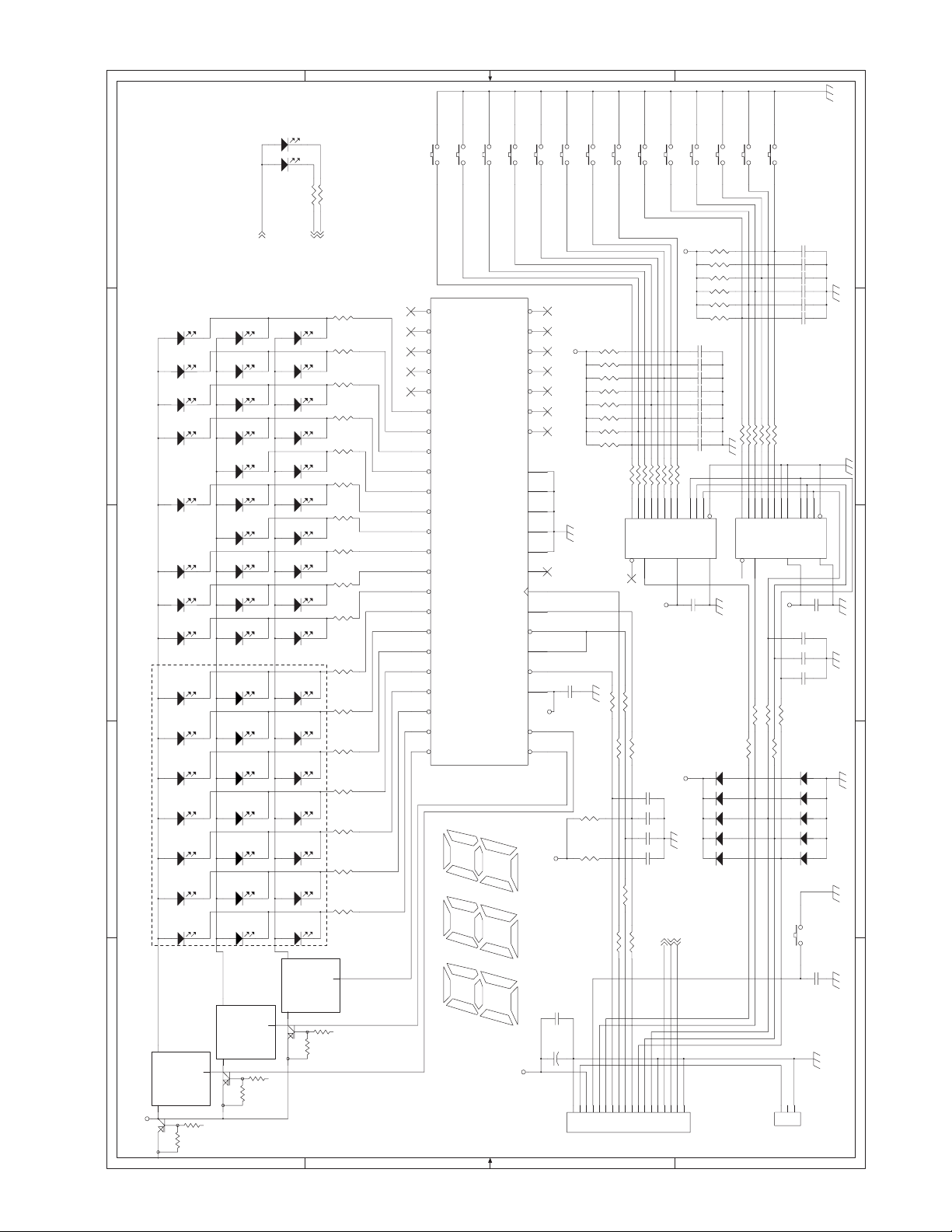
ONLL
PML
E
R354 470J
R353 470J
OLK
SCNK
MAGK
ZDWK
CLK
ZUPK
10UPK
1UPK
EXUPK
EXDWK
EXMODK
DUPK
CRSK
BPK
E
4.7KJ
R336 100J
5
C327
C326
C317
C319
SELIN2
R302 100J
R319 100J
200PF
200PF
200PF
200PF
SELIN3
D-GND
+5V
R327 100J
5VEN
5VEN
+5V
R307
4.7KJ
R305
4.7KJ
R316
4.7KJ
R315
4.7KJ
R311
4.7KJ
R306
1000p
C302
1000p
C314
1000p
C303
1000p
C312
1000p
C304
1000p
C316
1000p
C315
1000p
C313
R321 100J
R324 100J
12
A11B10C9G
VCC
C311
0.1uF
+5V
D303
1SS133
D306
1SS133
D307
1SS133
ONL
PSL
ONL
PSL
D-GND
18FE-ST-VK-N
7
GND
74HC151
D302
1SS133
D310
1SS133
IC302
R313 100J
R312 100J
R308 100J
R314 100J
R310 100J
R309 100J
D04D13D22D31D415D514D613D7
W6Y
5
R317 1KJ
R362 510J
R356 510J
R357 1KJ
CN302
ONL
Q302
KRA225S
2
PSL
R361
120J
2ENR
1ENR
NOR
1RE
2RE
3RE
CS2L
SPFL
SJAL
DAA2
3
1
R348
120J
R347
120J
R346
120J
R344
120J
R345
120J
R349
120J
R343
120J
R342
120J
R341
120J
R330
120J
a1
R328
120J
b1
R333
120J
c1
R329
120J
d1
R334
120J
e1
R332
120J
f1
R331
120J
g1
2
/Q8
39
/Q15
47
/Q14
46
/Q13
45
/Q12
43
/Q26
11
/Q25
10
/Q24
9
/Q23
8
/Q22
7
/Q21
6
/Q20
4
/Q19
3
/Q18
2
/Q17
1
/Q11
42
/Q10
41
/Q9
40
/Q7
38
/Q6
37
/Q5
36
/Q4
34
/Q3
33
IC303
LC7935AN
b3
a3
g3
f3
b2
a2
g2
f2
b1
a1
g1
f1
/Q16
48
/Q32
18
/Q27
12
13
15
16
17
62
44
35
14
5
19
64
30
50
49
51
63
31
32
LEDM
+5V
+5V
C325
C301
+5V
C318
22000PF
R359
R304
22000PF
47uF/16V
DRST
D-GND
123456789
CN301
/Q28
/Q29
/Q30
/Q31
GND5
GND4
GND3
GND2
GND1
S OUT
CLOCK
S IN
/LATCH
BEO
/STROBE
VCC
/Q1
/Q2
c3
d3
e3
c2
d2
e2
c1
d1
e1
+5V
4.7KJ
R323
4.7KJ
R325
4.7KJ
R301
4.7KJ
R320
4.7KJ
R303
4.7KJ
R337
4.7KJ
R326
4.7KJ
R355
R322 100J
R318 100J
D04D13D22D31D415D514D613D7
W6Y
IC301
R335 1KJ
R338 1KJ
R360 1KJ
R340 1KJ
1.5KJ
1.5KJ
R351 150J
R350 150J
R358 150J
OP-CLK
OP-DATA
OP-LATCH
KIN1
KIN2
PSW
OP-STB
SELIN1
101112131415161718
5V
5VEN
RPL
TPL
D
C
ZPL
AE
ME
PE
DU22
DU21
a3
b3
c3
d3
SCNL
BPL
CS1L
EXL
EXN
EXD
JPL
N.M.(MPL)
DPL
DAA1
a2
b2
c2
d2
B
e3
f3
g3
LEDM
A
3
Q303
KRA225S
1
+5V
Q301
3
KRA225S
1
2
e2
f2
g2
R352 1KJ
DRST
12
123
+5V
VCC
1000p
1000p
1000p
C320
C321
C322
D-GND
C305
C309
C307
A11B10C9G
1000p
C306
1000p
C310
1000p
C308
7
GND
C323
0.1uF
N.M.
N.M.
N.M.
D304
1SS133
D309
1SS133
PSW
C324
N.M.
S3B-PH-K-S
74HC151
D301
1SS133
D305
1SS133
D308
1SS133
D
C
B
A
2. OPERATION PWB
4 4
3 3
AR-5012 CIRCUIT DIAGRAM 14 - 10
2 2
1 1
Page 94
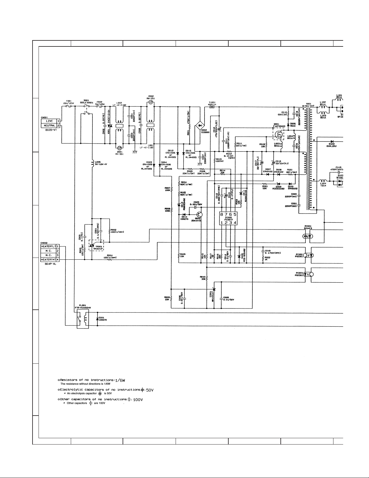
3. POWER SUPPLY
1
POWER SUPPLY (120V/127V)
A
B
C
2 3 4 5 6
D
E
F
G
H
1 2 3 4 5 6
AR-5012 CIRCUIT DIAGRAM 14 - 11
Page 95
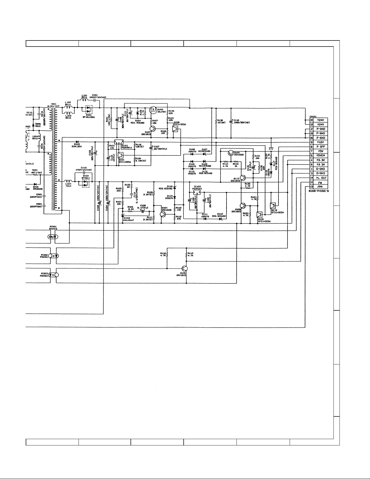
6 7 8 9 10 11
A
B
C
D
E
F
G
6 7 8 9 10 11
AR-5012 CIRCUIT DIAGRAM 14 - 12
H
Page 96

1
POWER SUPPLY (220V/240V)
A
B
C
2 3 4 5 6
D
E
F
4. NOISE FILTER CIRCUIT
G
H
1 2 3 4 5 6
AR-5012 CIRCUIT DIAGRAM 14 - 13
Page 97

6 7 8 9 10 11
A
B
C
D
E
F
G
6 7 8 9 10 11
AR-5012 CIRCUIT DIAGRAM 14 - 14
H
Page 98

5. ACTUAL WIRING DIAGRAM
10
S
S
G
G
G
C
/
G
G
/
/SYNC
/
O
SHO
G
CC
S
CO
O
O
O
C
SUS
/
/
/
/S
/
S
SLC
G
G
G
G
/
/SLC
G
(
)
ACTUAL WIRING DIAGRAM 1/7
*E
*C
interface
(POLYGON MT)
PPD2 sensorPWB 1
Thermisto
PWB
(GDI)
USB
LSU
PULUP5V
PPD2
2 CN120
D-
ND
3
RTH_IN
1
ND
D-
2
Fuser unit
CN104
D-GND
1
D-
2
V
3
EN5V
4
EN5V
5
BIN
U
6
D_
7
VP
8
VM
9
EN
10
R
V
11
VPIN
12
VMIN
13
14
PARAD0
15
PARAD1
16
PARAD2
17
PARAD3
18
PARAD4
19
PARAD5
20
PARAD6
21
PARAD7
22
REV
23
FAULT
24
ACK
25
BU
26
PE
27
28
INT
29
30
AUTOFD
31
TB
32
DIIN
33
D-
34
D-
35
35FE-BT-VK-N
CN119
1
INT5V
2
D-GND
3
4
VIDE
5
6
D-
7
LDEN
8
9
10
D-
11
D-
12
ND
P-
13
PM
14
PMRDY
15
PMD
16
P-
ND
17
24V
18
B18B-PHDSS-B
PULUP5V
1
2
PPD2
D-GND
3
RTH_IN
4
5
D-GND
B5B-PH-K-
ND
3
UT
PEND
Y
T
TIN
ND
ND
LD
ND
ND
ND
LK_A
Paper out
detecter
123
PULUP5V
POD
D-GND
B3B-PH-K-S
CN113
NT
UT
Resist roller
Solenoide
123
24V
/RRS
B3B-PH-K-B
CN117
Cassette paper
Solenoide
123
24V
/CPFS1
B3B-PH-K-S
CN110
Cassette detect
123
CED1
D-GND
D-GND
B3B-PH-K-K
CN108
B14B-PHDSS-B
2nd
cassette
123456789
/CPFS2
24V
5V
PPD3
D-GND
1011121314
CED2
D-GND
D-GND
D-GND
CN115
MCU
CN123
24V
1
/MPFS
2
PULUP5V
3
MFD
4
D-GND
5
B5B-PH-K-R
B4B-PH-K-S
VFMOUT
123
FAN
MT
/VFMCNT
PGND
4
CN112
B2P-VH-S
TMB-
TMA-
CN124
1
2
TONER
MT
08FE-BT-VK-N
MMLD
PGND
PGND
1234567
PGND
/MMD
MAIN
MT
PGND
INT24V
INT24V
8
CN107
B5B-XASK-1
/DMT_1
/DMT_0
24Vdup
12345
DUPLEX
/DMT_2
/DMT_3
CN114
B24B-PHDSS-B
D-GND
123456789
SPPD
D-GND
PULUP5V
SPID
SDSW
MT
For DSPF Model Only For
SB4D
5V
*F
Manual Paper
Feeding unit
AR-5012 CIRCUIT DIAGRAM 14 - 15
Page 99

S
(
)
)
)
)
)
*E
Cassette detect
123
CED1
D-GND
D-GND
B3B-PH-K-K
CN108
cassette
123456789
/CPFS2
24V
5V
B14B-PHDSS-B
MCU
2nd
PPD3
D-GND
1011121314
D-GND
D-GND
CED2
D-GND
CN115
Paper pass detect
123
PULUP5V
PPD1
D-GND
B3B-PH-K-R
CN111
Scanner
MT
123
4
OUT_A+
OUT_B+
OUT_A-
OUT_B-
B4B-PH-K-R
CN103
CN102
D-GND
(ONL
(PSL
EN5V
D-GND
SELIN3
SELIN2
SELIN1
OP-DATA
OP-LATCH
OP-CLK
(BEO)
(KIN1
(KIN2
DRST
D-GND
18FE-BT-VK-N
CN105
PGND
PGND
EN5V
D-
VSAMP
CCD-TG
D-GND
CCD-RS
BSAMP
CCD-CP
AFE_SDI
CCD-PHI2
D-GND
CCD-PHI1
AFE_SEN
ADCLK
D-GND
AFE_SCK
AFE_DB7
mt_at_home
AFE_DB5
AFE_DB6
D-GND
AFE_DB4
AFE_DB3
AFE_DB2
AFE_DB1
AFE_DB0
15D5
FE4-32-
PSW
GND
1
2
3
4
5
6
7
8
9
10
11
12
13
14
15
5V
16
17
18
1
2
VCL
3
VCL
4
12V
5
12V
6
7
8
9
10
11
12
13
14
15
16
17
18
19
20
21
22
23
24
25
26
27
28
29
30
31
32
Operational PWB
Scanner
(CCD)
*B
*B
B5B-XASK-1
/DMT_0
24Vdup
12345
/DMT_1
/DMT_2
/DMT_3
CN114
B24B-PHDSS-B
PULUP5V
D-GND
D-GND
SPPD
SPID
123456789
SDSW
/SPUS
SB4D
/SPFS
24V
5V
101112131415161718192021222324
DUPLEX
MT
For DSPF Model Only For SPF/DSPF Model Only
SPF
UNIT
CN106
1
24V
TCS
2
DVSEL
3
D-GND
4
B4B-PH-K-R
CN101
1
INT24V
2
3
4
/BIAS
5
/TC
6
/GRIDL
7
/MC
8
D-
GND
9
PGND
10
D-GND
11
3.3VIN
12
5VEN
13
3.3VIN
14
5VIN
15
/POFF
16
12VIN
17
24VIN
18
FW
19
24VIN
20
/PR
21
HLOUT
22
PGND
23
PGND
24
B24B-PHDSS-B
24VM
24VM
CN122
B3B-PH-K-S
5V
123
(SDOD)
D-GND
CN109
SPMT-0
SPMT-2
SPMT-3
SPMT-1
/SRRC
/SGS
24V
24V
24V
Cover open
detecter
24V1(DSWS)
B2P-VH-R
CN116
24V
1
2
INTERLOCK SW
(SIDE DOOR SW)
DV
*A
Power
unit
*A – E have detail view
For DSPF Model Only
*D
AR-5012 CIRCUIT DIAGRAM 14 - 16
Page 100
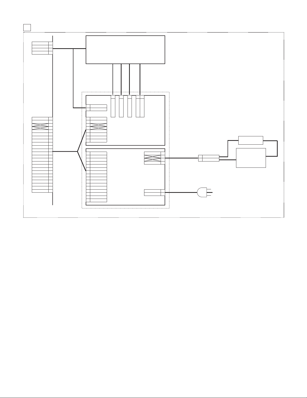
ACTUAL WIRING DIAGRAM 2/7 (POWER UNIT)
A
CN106
24V
1
TCS
2
DVSEL
3
D-GND
B4B-PH-K-R
INT24V
INT24V
/BIAS
/TC
/GRIDL
/MC
D-GND
PGND
D-GND
3.3VIN
5VEN
3.3VIN
5VIN
/POFF
12VIN
24VIN
FW
24VIN
/PR
HLOUT
PGND
PGND
B24B-PHDSS
4
CN101 CN6
1
2
3
4
5
6
7
8
9
10
11 CN101 CN002
12 1 1
13 2 2 1
14 3 3 2
15 4 4
16 5
17 6
18 7
19 8
20 9
21 10
22 11
23 12 CN001
24 13 1 AC-ORD
CN10
1
DV-BIAS
2
F-GND
INT24V
1
INT24V
2
3
4
/BIAS
5
/TC
6
/GRIDL
7
/MC
8
D-GND
PGND
D-GND
3.3VIN
5VEN
3.3VIN
5VIN
/POFF
12VIN
24VIN
FW
24VIN
/PR
HLOUT
14 2
PGND
15
PGND
16
DV UNIT
1
1
TC-OUT
MC-OUT
HIGH VOLTAGE
POWER SUPPLY UNIT
LOW VOLTAGE
POWER SUPPLY UNIT
1
BC-OUT
1
2
GRID
MC-CASE
HLL
HLN
L
N
HLL
HLN
Thermostat
Heater
Lamp
POWER UNIT
AR-5012 CIRCUIT DIAGRAM 14 - 17
 Loading...