


®
VNQ860
/ VNQ860S P
QUAD CH ANNEL HIGH SIDE DRIV ER
6P
TYPE R
VNQ860
VNQ860SP
(*) Per each channel
■ CMOS COMPATIBLE I/Os
■ UNDERVOLTAGE & OV ERVOLTAGE
SHUT- DOWN
n
■ SHORTED LOAD PROTECTION
■ THERMAL SHUTDOWN
■ VERY LOW STAND-BY CURRENT
■ PROTECTION AGAINST LOSS OF GROUND
DS(on)
(*) I
OUT
V
CC
270mΩ 0.25A 36V
DESCRIPTION
The VNQ860, VNQ86 0SP are mono lithic devi ces
made using| STMicroelectronics VIPower M0-3
Technology, intended for driving any kind load
with one side connected to ground. Active current
limitation combined with thermal shutdown and
automatic restart protect the device against
overload. Device automatically turns off in case of
ground pin disconnection. This device is
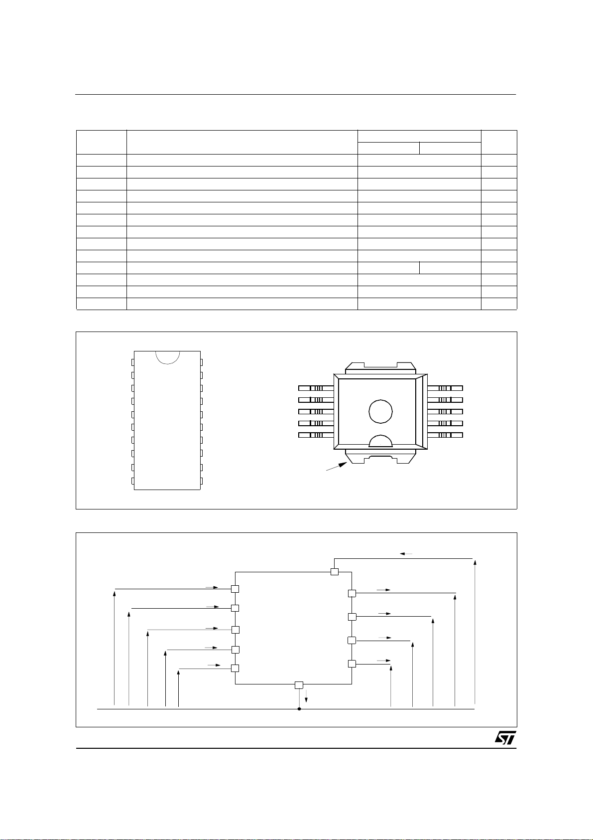
BLO C K DIAGRA M
10
1
SO-20
PowerSO-10™
ORDER CODES
SO-20
PowerSO-10™
VNQ860
VNQ860SP
especially suitable for industrial applications in
norms conformity with IEC1131 (Programmable
Controllers International Standard).
V
CC
OUTPUT1
OUTPUT2
OUTPUT3
OUTPUT4
GND
I/O 1
I/O 2
I/O 3
I/O 4
STATUS
V
CC
CLAMP
LOGIC
OVERVOLTAG E
UNDERVOLTAGE
OVERTEMP
OVERTEMP
OVERTEMP
OVERTEMP
DETECTION
DETECTION
Power CLAMP
CURRENT LIMITER
Power CLAMP
CURRENT LIMITER
Power CLAMP
CURRENT LIMITER
Power CLAMP
CURRENT LIMITER
Januar y 20 03 1/10
1
VNQ860 / VNQ860SP
ABSOLUTE MAXIMUM RATING
Symbol Parameter
tot
DC supply voltage 41 V
Reverse DC supply volt age - 0.3 V
CC
DC reverse ground pin current - 200 mA
DC output current Internally Limited A
Reverse DC output current - 2 A
DC Input current +/- 10 mA
Input voltage range -3/+V
IN
DC Status voltage + V
Electrostatic discharge (R=1.5 KΩ; C=100 pF) 2000 V
Power dissipation TC=25 °C 16 90 W
Junction operating temperature Internally Limited °C
j
Case operating temperature - 40 to 150 °C
c
Storage t em perature - 55 to 150 °C
1
10
20
11
GROUND
I/O 3
OUTPUT 3
V
CC
V
CC
V
CC
V
CC
N.C.
OUTPUT 2
I/O 2
V
CC
- V
- I
GND
I
OUT
- I
OUT
I
IN
V
V
STAT
V
ESD
P
T
T
T
stg
CONNECTION DIAGRAM
I/O 4
OUTPUT 4
N.C.
V
CC
V
CC
V
CC
V
CC
OUTPUT 1
I/O 1
STATUS
OUTPUT 3
I/O 3
GND
I/O 4
OUTPUT 4
Value
SO-20 PowerSO-10
CC
CC
6
7
8
9
10
TAB
V
CC
5
4
3
2
1
Unit
V
V
OUTPUT 2
I/O 2
STATUS
I/O 1
OUTPUT 1
CURRENT AND VOLTAGE CONVENTIONS
I
I/O1
V
I/O1
V
I/O2
V
I/O3
V
I/O4
V
STAT
I
I/O2
I
I/O3
I
I/O4
I
STAT
I/O1
I/O2
I/O 3
I/O 4
STATUS
2/10
1
GND
V
CC
OUTPUT 1
OUTPUT 2
OUTPUT 3
OUTPUT 4
I
GND
I
OUT1
I
OUT2
I
OUT3
I
OUT4
V
OUT4
V
OUT3
V
I
CC
OUT2
V
OUT1
V
CC
VNQ860 / VNQ860SP
THERMAL DATA
Symbol Parameter
R
R
R
tj-amb
tj-case
tj-pin
Therma l resistance junction -pins (MAX) 8 Therma l resistance junction -ambient (*) (MAX) 58 50
Therma l resistance junction -case (MAX) - 1.4
SO-20 PowerSO-10
(*) When mounted on FR4 printed circuit board with 0.5 cm2 of copper area (at least 35µ thick) connected to all VCC pins.
ELECTRICAL CHARACTERISTICS (8V<VCC<36V; -40oC<Tj<150oC; unless otherwise specified)
POWER
Symbol Parameter Test Conditions Min Typ Max Unit
V
CC
V
USD
V
OV
R
ON
I
S
I
LGND
I
L(off)
I
OUTleak
I
OUTleak
Operating supply voltage 5.5 36 V
Undervolt age shut-down 3 4 5.5 V
Overvoltage shut-down 36 42 48 V
On state resistance
(per ch annel)
Supply current
Output current
Off state output current VIN=V
Off state output leakage
current
Off state output leakage
current
I
=0.25A ; Tj=25oC
OUT
I
=0.25A
OUT
Off state;
V
=24V; Tc=25oC
CC
On state (all channels on)
V
CC-VSTAT=VIN=VGND
V
=0V
OUT
V
IN=VGND
T
amb
V
IN=VGND
V
OUT
=0V 0 10 µA
OUT
=0V; VCC=V
=25oC
=0V; VCC=24V;
=10V; T
amb
=24V
OUT
=25oC
=24V;
Value
70
5
Unit
o
C/W
o
C/W
o
C/W
270
540
120
10
mΩ
mΩ
µA
mA
1mA
240 µA
100 µA
SWITCHING (VCC=24V) (Per channel)
Symbol Par am eter Test Conditions Min Typ Max Unit
Turn-on delay time
Turn-off delay time
/dt)onTurn-on voltage slo pe RL=96Ω from V
/dt)
Turn-off voltage slope RL=96Ω from V
off
(dV
(dV
t
D(on)
t
D(off)
OUT
OUT
RL=96Ω from VIN rising edge to
V
=2.4V
OUT
RL=96Ω from VIN falling edge to
V
=21.6V
OUT
=2.4V to 19.2V 0.75 V/µs
OUT
=21.6V to 2.4V 0.2 5 V/µs
OUT
10 µs
40 µs
PROTECTIONS (Per channel)
Symbol Parameter Test Conditions Min Typ Max Unit
Current limitation 0.35 0.7 1.1 A
Thermal hysteresis 7 15
Thermal shut-down
temperature
150 175 200
Reset temperature 135
Turn-off output clamp voltage I
=0.25A VCC-47 VCC-52 VCC-59 V
OUT
T
T
V
demag
I
lim
(hyst)
TSD
T
R
o
o
o
C
C
C
3/10
1

VNQ860 / VNQ860SP
ELECTRICAL CHARACTERISTICS (continued)
LOGIC INPUT (Per channel)
Symbol Parameter Test Conditions Min Typ Max Unit
V
IL
I
IL
V
IH
I
IH
V
I(hyst)
I
IN
V
OL
STATUS PIN
Symbol Parameter Test conditions Min Typ Max Unit
V
STAT
I
LSTAT
C
STAT
TRUTH TABLE
CONDITIONS MCOUTn I/On OUTPUTn STATUS
Normal op eration
Current limit ati on
Overtemperature
Undervoltage
Overvoltage
Low level input voltag e 1.25 V
Low level input curr ent VIN=1.25V 1 µA
High level input v oltage 3.25 V
High level i n put current VIN=3.25V 10 µA
Input hysteresis Voltage 0.5 V
Input curren t VIN=VCC=36V 200 µA
I/O Output voltage IIN=5mA (Faul t condition) 1 V
Status lo w output voltage I
Status leakage current Normal operation; V
Status pin input cap acitance Normal operation; V
L
H
L
H
L
H
L
H
L
H
=5mA (Fau lt co nd i tion) 1 V
STAT
STAT=VCC
STAT
L
H
L
H
L
Driven low
L
H
L
H
=36V 10 µA
=5V 100 pF
L
H
L
X
L
L
L
L
L
L
H
H
H
H
L
L
X
X
H
H
4/10
2

SWITCHING CHARACTE RISTICS
V
OUT
/dt)
OUT
VNQ860 / VNQ860SP
80%
on
t
r
10%
90%
t
f
(dV
OUT
/dt)
off(dV
t
V
IN
Typical application schematic
MCOUTn
MCINn
MCU
t
d(on)
I/On
t
d(off)
OUTPUTn
VNQ860
t
5/10
1

VNQ860 / VNQ860SP
Figur e 1: Waveforms
V
I/On
V
OUTn
V
STAT
V
V
V
V
CC
I/On
OUTn
STAT
V
USD
NORMAL OPERATION
UNDERVOLTA GE
V
USDhyst
undefined
V
V
V
V
V
I
CC
I/On
OUTn
STAT
T
V
OUTn
V
T
TSD
T
R
j
MCOUT
I/On
STAT
VCC>V
V
USD
OVERVOLTAG E
OV
V
OVhyst
OVERTEMPERATURE
6/10
1

SO-20 MECHANICAL DATA
VNQ860 / VNQ860SP
DIM.
A 2.65 0.104
a1 0.10 0.20 0.004 0.007
a2 2.45 0.096
b 0.35 0.49 0.013 0.019
b1 0.23 0.32 0.009 0.012
C 0.50 0.020
c1 45° (typ.)
D 12.60 13.00 0.496 0.512
E 10 .00 10.65 0.393 0.419
e 1.27 0.050
F 7.40 7.60 0.291 0.299
L 0.50 1.27 0.19 0.050
M 0.75 0.029
S8° (max.)
MIN. TYP M AX. MIN. TYP . MAX.
mm. inch
7/10

VNQ860 / VNQ860SP
PowerSO-10™ MECHANICAL DATA
DIM.
MIN. TYP MAX. MIN. TYP. MAX.
mm. inch
A 3.35 3.65 0.132 0.144
A (*) 3.4 3.6 0.134 0.142
A1 0.00 0.10 0.000 0.004
B 0.40 0.60 0.016 0.024
B (*) 0.37 0.53 0.014 0.021
C 0.35 0.55 0.013 0.022
C (*) 0.23 0.32 0.009 0.0126
D 9.40 9.60 0.370 0.378
D1 7.40 7.60 0.291 0.300
E 9.30 9.50 0.366 0.374
E2 7.20 7.60 0.283 300
E2 (*) 7.30 7.50 0.287 0.295
E4 5.90 6.10 0.232 0.240
E4 (*) 5.90 6.30 0.232 0.248
e 1.27 0.050
F 1.25 1 .35 0.049 0.053
F (*) 1.20 1.40 0.047 0.055
H 13.80 14.40 0.543 0.567
H (*) 13.85 14.35 0.545 0.565
h 0.50 0.002
L 1.20 1.80 0.047 0.070
L (*) 0.80 1.10 0.031 0.043
α 0º 8º 0º 8º
α (*) 2º 8º 2º 8º
(*) Muar only POA P013P
8/10
HE
h
A
F
A1
10
1
eB
0.25
D
= =
D1
= =
E2
DETAIL "A"
DETA IL "A"
B
0.10 A
SEATING
PLANE
A
C
α
B
E4
SEATING
PLANE
A1
L
P095A

VNQ860 / VNQ860SP
PowerSO-10™ SUGGESTED PAD LAYOUT
14.6 - 14.9
10.8 - 11
6.30
0.67 - 0.73
1
2
3
9.5
4
5
10
0.54 - 0.6
9
8
7
1.27
6
TAPE AND REEL SHIPMENT (suffix “1 3TR”)
TUBE SHIPMENT (no suffix)
C
A
B
A
All dimensi ons ar e in mm.
Base Q.ty Bulk Q.ty Tube length (± 0.5) A B C (± 0.1)
Casablanca 50 1000 532 10.4 16.4 0.8
Muar 50 1000 53 2 4.9 17.2 0.8
MUARCASABLANCA
B
REEL DIMENSIONS
Base Q.ty 600
Bulk Q.ty 600
A (max) 330
B (min) 1.5
C (± 0.2) 13
F 20.2
G (+ 2 / -0) 24.4
N (min) 60
T (max) 30.4
C
TAPE DIMENSIONS
According to Electronic Industries Association
(EIA) Standard 481 rev. A, Feb. 198 6
Tape width W 24
Tape Hole Spacing P0 (± 0.1) 4
Component Spacing P 24
Hole Diameter D (± 0.1/-0) 1.5
Hole Diameter D1 (min) 1.5
Hole Position F (± 0.05) 11.5
Compartm ent Depth K (max) 6.5
Hole Spacing P1 (± 0.1) 2
All dimensions are in mm.
Top
cover
tape
End
500mm min
All dimensions are in mm.
Empty components pockets
saled with cover tape.
User direction of feed
Start
No componentsNo components Components
500mm min
9/10
1

VNQ860 / VNQ860SP
Information furnished is believed to be a c c ur ate and reliab le. However, STMicroelectronics ass um es no responsibility for the consequences
of use of such information nor for any infringement of patents or other rights of third parties which may results from its use. No license is
granted by implication or oth er wise under any patent or patent r ights of STMicroelectronics . Specificatio ns m entioned in this publication are
subject to c hange without notice. This publication s upersedes an d r eplaces all information p r ev iously suppl ied. STMicroelectronic s pr oducts
are not authorized for use as critical components in life support devices or systems without express written approval of STMicroelectronics.
Australia - Brazil - Canada - China - Finland - France - Germany - Hong Kong - India - Isra el - Italy - Japan - M alaysia -
Malta - Morocco - Singapore - Spain - Sweden - Switzerland - United Kingdom - U.S.A.
The ST logo is a trademark of STM ic r oelectronics
2003 STMicroelectronics - Printed in ITALY- All Rights Reserved.
STMicroelectronics GROUP OF COMPANIES
http://www.st.com
10/10
 Loading...