

VND670SP
DUAL HIGH SIDE SWITCH WITH DUAL POWER MOS
GATE DRIVER (BRIDGE CONFIGURATION)
TYPE R
DS(on)
I
OUT
V
DSS
VND670SP 30 mΩ 15 A 40 V
■ OUTPUT CURRENT:15A PER CHANNEL
■ 5V LOGIC LEVEL COMPATIBLE INPUTS
■ GATE DRIVE FOR TWO EXTERNAL POWER
MOS
■ UNDERVOLTAGE AND OVERVOLTAGE
SHUT-DOWN
■ OVERVOLTAGE CLAMP
■ THERMAL SHUT DOWN
■ CROSS-CONDUCTION PROTECTION
■ CURRENT LIMITATION
■ VERY LOW STAND-BY POWER
CONSUMPTION
■ PWM OPERATION UP TO 10 KHz
■ PROTECTION AGAINST:
LOSS OF GROUND AND LOSS OF V
■ REVERSE BATTERY PROTECTION (*)
CC
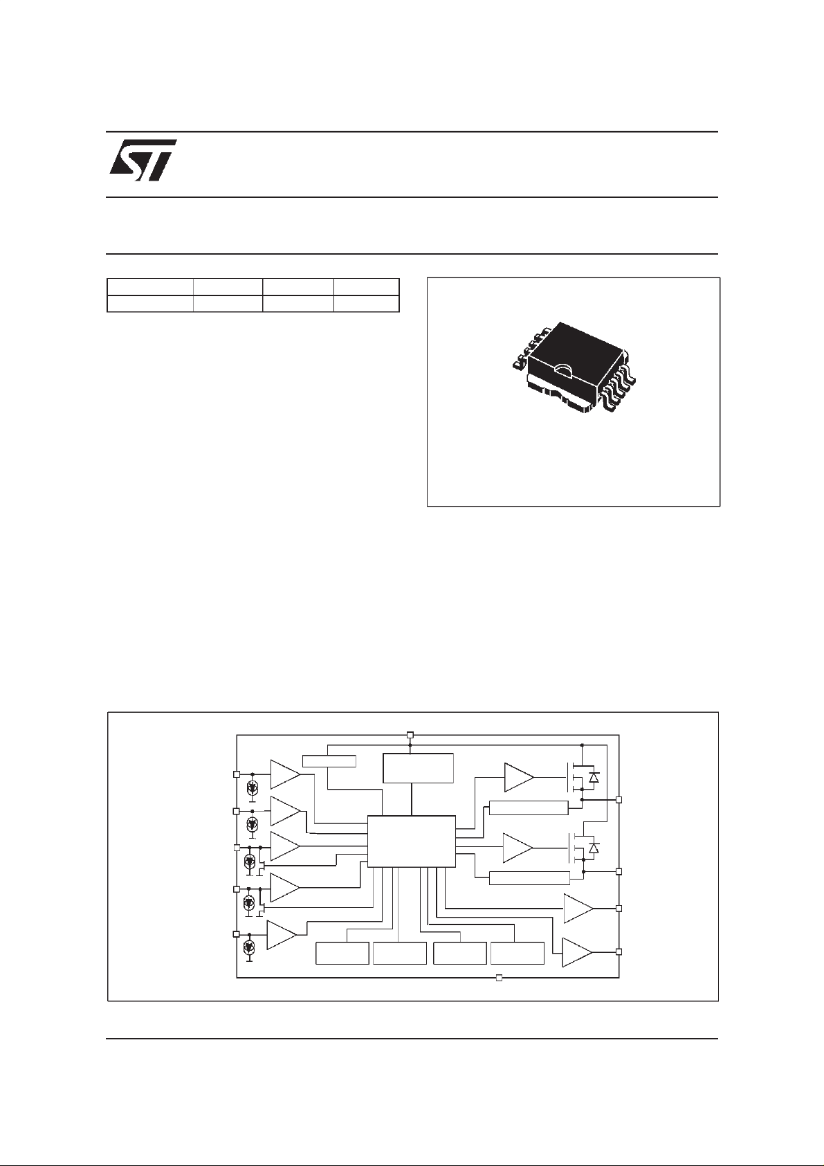
DESCRIPTION
The VND670SP is a monolithic device made
using STMicroelectronics VIPower technology,
intended for driving motors in full bridge
BLOCK DIAGRAM
10
1
PowerSO-10
configuration. The device integrates two 30 m
Power MOSFET in high side configuration, and
provides gate drive for two external Power
MOSFET used as low side switches.IN
allow to select clockwise or counter clockwise
and IN
A
drive or brake; DIAGA/ENA, DIAGB/ENBallow to
disable one half bridge and feedback diagnostic.
Built-in thermal shut-down, combined with a
current limiter, protects the chip in
overtemperature and short circuit conditions.
Short to battery protects the external connected
low-side Power MOSFET.
V
CC
Ω
B
DIAGA/EN
DIAG
PWM
(*) See note at page 5
IN
A
IN
B
A
/EN
B
B
Undervolt.
Overtemp.AOvertemp.
INTERNAL
SUPPLY
LOGIC
B
Current
Limiter B
Short to battery
Short to battery
Current
Limiter A
GND
OUT
OUT
GATE
GATE
A
B
A
B
June 2000 1/13
1
VND670SP
ABSOLUTE MAXIMUM RATING
Symbol Parameter Value Unit
V
I
max1
I
max2
I
I
I
EN
I
pw
I
gs
V
ESD
T
T
STG
CURRENT AND VOLTAGECONVENTIONS
Supply voltage -0.3 .. 40 V
CC
Maximum output current (continuous) 15 A
Maximum output current (250 ms pulse duration) 20 A
Reverse output current (continuous) -15 A
R
Input current +/- 10 mA
IN
Enable pin current +/- 10 mA
PWM pin current +/- 10 mA
Output gate current +/- 20 mA
Electrostatic discharge (R=1.5kΩ, C=100pF) 2000 V
Junction operating temperature -40 to 150 °C
j
Storage temperature -55 to 150 °C
I
CC
I
INA
I
INB
I
ENA
I
ENB
IN
A
IN
B
DIAGA/EN
DIAGB/EN
I
pw
PWM
V
CC
OUT
A
OUT
B
A
B
GATE
GATE
GND
A
B
I
gsB
I
gsA
V
gsB
I
V
OUTB
gsA
I
OUTA
V
OUTB
V
OUTA
V
CC
V
V
INA
INB
V
ENB
V
pw
V
ENA
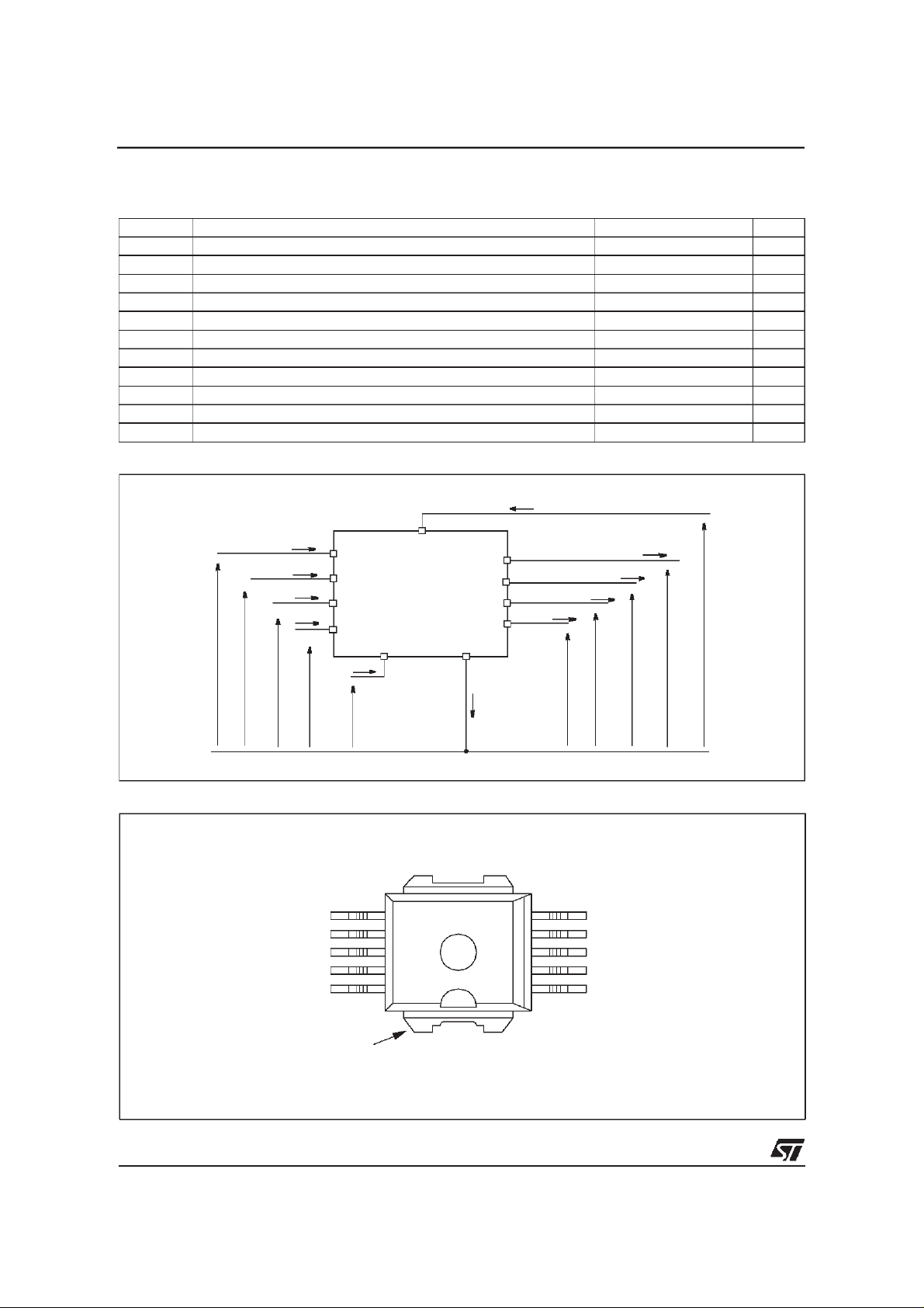
CONNECTION DIAGRAM (TOP VIEW)
INPUT B
DIAG
/EN
B
A
/EN
B
A
V
CC
PWM
DIAG
INPUT A
10
I
GND
6
7
8
9
5
4
3
2
1
OUTPUT B
GATEB
GROUND
GATEA
OUTPUT A
11
2/13
1
VND670SP
THERMAL DATA
Symbol Parameter Value Unit
R
thj-case
R
thj-amb
(*) When mounted using the recommended pad size on FR-4 board (See AN515 Application Note).
ELECTRICAL CHARACTERISTICS (VCC=9V up to 18V; -40°C<Tj<150°C; unless otherwise specified)
POWER
Symbol Parameter Test Conditions Min Typ Max Unit
V
CC
R
ON
I
s
V
gate
V
gs,cl
Thermal resistance junction-case (per channel) (MAX) 1.4 °C/W
(*) Thermal resistance junction-ambient (MAX) 50 °C/W
Operating supply voltage 5.5 26 V
On state resistance
Supply current
=12A
I
LOAD
I
=12A; Tj=25oC26
LOAD
ON state
OFF state
50
30
15
40
mΩ
mΩ
mΑ
µA
Gate output voltage 5.0 8.5 V
Gate output clamp voltage Igs=-1 mA 6.8 7.4 8.5 V
SWITCHING (VCC=13V, R
LOAD
=1.1Ω)
Symbol Parameter Test Conditions Min Typ Max Unit
(dV
(dV
t
D(on)
t
D(off)
OUT
OUT
t
dong
t
t
doffg
t
t
del
t
r
t
f
/dt)
/dt)
rg
fg
Turn-on delay time
50 150 µs
Turn-on delay time 45 135 µs
Output voltage rise time 50 150 µs
Output voltage fall time 40 120 µs
Turn-on voltage slope 160 500 V/ms
on
Turn-off voltage slope 230 1200 V/ms
off
VgsTurn-on delay time
Vgsrise time 2.6 10 µs
VgsTurn-off delay time 1.0 5.0 µs
Vgsfall time 2.2 10 µs
External MOSFET turn-on
dead time
Input rise time < 1µs (see fig. 1)
C1=4.7nF
0.5 2 µs
Break to ground configuration
(see fig. 2)
(see fig. 3) 600 1800 µs
150
PROTECTION AND DIAGNOSTIC
Symbol Parameter Test Conditions Min Typ Max Unit
V
V
T
V
USD
I
LIM
TSD
V
OV
ocl
sat
Undervoltage shut-down 5.5 V
Overvoltage shut-down 36 43 V
Current limitation 30 45 A
Thermal shut-down
temperature
Output turn-off clampvoltage
External MOSFET saturation
voltage detection threshold
V
= 3.25 V 150 170 200 °C
IN
=12A, L=6mH
I
LOAD
V
-55 VCC-41 V
CC
2.5 4.2 5.5 V
3/13
1
VND670SP
ELECTRICAL CHARACTERISTICS (continued)
PWM
Symbol Parameter Test Conditions Min Typ Max Unit
V
pwl
I
pwl
V
pwh
I
pwh
V
pwhhyst
V
pwcl
V
pwtest
I
pwtest
LOGIC INPUT (INA/INB)
Symbol Parameter Test Conditions Min Typ Max Unit
V
IL
I
INL
V
IH
I
INH
V
IHYST
V
ICL
PWM low level
voltage
1.5 V
PWM pin current Vpw=1.5V 1 µA
PWM high level
voltage
3.25 V
PWM pin current Vpw=3.25V 10 µA
PWM hysteresis voltage 0.5 V
PWM clamp voltage
I
pw
I
pw
=1mA
=-1mA
V
CC
-5.0
+0.3
VCC+0.7
-3.5
VCC+1.0
-2.0
Test modePWM pin voltage -3.5 -2.0 -0.5 V
Test modePWMpin current V
= -2.0 V -2000 -500 µA
pwtest
Input low level voltage 1.5 V
Input current VIN=1.5 V 1 µA
Input high level voltage 3.25 V
Input current VIN=3.25 V 10 µA
Input hysteresis voltage 0.5 V
Input clamp voltage
I
IN
I
IN
=1mA
=-1mA
6.8
-1.0
7.4
-0.7
8.5
-0.3
V
V
V
V
ENABLE (LOGIC I/O PIN)
Symbol Parameter Test Conditions Min Typ Max Unit
Normal operation
V
I
V
I
ENH
V
EHYST
V
ENCL
V
ENL
ENL
ENH
DIAG
Enable low level voltage
(DIAG
/ENXpin acts as an
X
input pin)
1.5 V
Enable pin current VEN= 1.5 V 1 µA
Normal operation
Enable high level voltage
/ENXpin acts as an
(DIAG
X
input pin)
3.25 V
Enable pin current VEN= 3.25 V 10 µA
Normal operation
Enable hysteresis voltage
Enable clamp voltage
/ENXpin acts as an
(DIAG
X
input pin)
=1mA
I
EN
IEN=-1mA
0.5 V
6.8
-1.0
7.4
-0.7
8.5
-0.3
Fault operation
Enable output low level
voltage
/ENXpin acts as an
(DIAG
X
input pin)
=1.6 mA
I
EN
0.4 V
V
V
4/13
2

VND670SP
WAVEFORMS AND TRUTH TABLE
TRUTH TABLE IN NORMAL OPERATING CONDITIONS
In normaloperating conditions the DIAGX/ENXpinis considered asan input pin by the device. Thispin must be externally
pulled high.
IN
A
IN
DIAGA/ENADIAGB/EN
B
OUT
B
OUT
A
GATE
B
GATE
A
B
1 1 1 1 H H L L Brake to V
1 0 1 1 H OPEN L H Clockwise
0 1 1 1 OPEN H H L Counter cw
0 0 1 1 OPEN OPEN H H Brake toGND
X X 0 0 OPEN OPEN L L Stand by
1 X 1 0 H OPEN L L HS
0 X 1 0 OPEN OPEN H L MOS
X 1 0 1 OPEN H L L HS
X 0 0 1 OPEN OPEN L H MOS
PWM pin usage:
In all cases,a “0” on the PWM pin will turn-off both GATE
GATE
turn on again depending on the input pin state.
B
and GATEBoutputs. When PWM rises back to “1”, GATEAor
A
TYPICAL APPLICATION CIRCUIT FOR DC TO 10KHz PWM OPERATION
R
prot
1K
DIAGA/EN
R1
A
+5V
V
CC
+5V
R1
DIAGB/EN
VND670SP
R
prot
1K
PWM
R
prot
1K
IN
A
GATE
OUT
A
A
UP
GND
R
gnd
(*)
OUT
B
IN
B
GATE
B
Comment
CC
only
A
only
A
only
B
only
B
R
prot
1K
B
R
prot
1K
M
DOWN
External Power Mos A
(*) Reverse battery protection:
- series relay in VCCline: R
- series fuse in VCCline with antiparallel diode between ground and VCC:R
=0 Ohms
gnd
External Power Mos B
=10 Ohms.
gnd
5/13

VND670SP
TYPICAL APPLICATION CIRCUIT FOR A 20KHZ PWM OPERATION
R
prot
1K
R
prot
1K
R
prot
1K
DIAGA/EN
IN
PWM
27Ω
+5V
R1
DIAGB/EN
R
prot
1K
B
R1
A
+5V
V
CC
VND670SP
OUT
A
GATE
A
A
R
(*)
gnd
UP
OUT
B
R
prot
1K
B
GATE
IN
B
M
D1
D2
DOWN
27Ω
External
Power Mos A
External
Power Mos B
(*) Reverse battery protection:
- series relay in VCCline: R
- series fuse in VCCline with antiparallel diode between ground and VCC:R
=0 Ohms
gnd
6/13
=10 Ohms.
gnd

VND670SP
WAVEFORMS AND TRUTH TABLE(CONTINUED)
In case of a fault condition the DIAGX/ENXpin is consideredas anoutput pin by the device.
The fault conditions are:
- overtemperature on one or both high sides;
- short to battery condition on theoutput (saturation detection on the external connected Power
MOSFET).
Possible origins of fault conditions may be:
OUT
is shorted to ground ---> overtemperature detection on high side A.
A
OUT
is shorted to VCC---> external Power MOSFET saturation detection (driven by GATEA).
A
When a fault condition is detected, the user can know which power element is in fault by monitoring the IN
EN
and DIAGB/ENBpins.
A
In any case, when a fault is detected, the faulty half bridge is latched off. To turn-on the respective output (GATE
OUT
) again, the input signal must rise from low to high level.
X
TRUTH TABLE IN FAULTCONDITIONS (detected on OUTA)
,INB, DIAGA/
A
or
X
IN
IN
A
B
DIAGA/EN
A
DIAGB/EN
B
OUT
A
OUT
B
GATE
A
1 1 0 1 OPEN H L L
1 0 0 1 OPEN OPEN L H
0 1 0 1 OPEN H L L
0 0 0 1 OPEN OPEN L H
X X 0 0 OPEN OPEN L L
1 X 0 0 OPEN OPEN L L
0 X 0 0 OPEN OPEN L L
X 1 0 1 OPEN H L L
X 0 0 1 OPEN OPEN L H
Fault Information
Protection Action
TEST MODE
The PWM pin allows to test the load connection between two half-bridges. In the test mode (V
Power Mos gate drivers are disabled. The IN
to connect one side of the load at V
continuity of the load connection. In case of load disconnection the DIAD
CC
pulled down.
orINBinputs allow to turn-on the High Side A or B, respectively, in order
A
voltage. The check of the voltageon the other side of the load allow to verify the
/ENXpin corresponding to the faulty output is
X
=-2V) the external
pwm
GATE
B
7/13
1

VND670SP
ELECTRICAL TRANSIENT REQUIREMENTS
ISO T/R
7637/1
Test Pulse
1 -25V -50V -75V -100V 2ms, 10Ω
2 +25V +50V +75V +100V 0.2ms, 10Ω
3a -25V -50V -100V -150V 0.1µs, 50Ω
3b +25V +50V +75V +100V 0.1µs, 50Ω
4 -4V -5V -6V -7V 100ms, 0.01Ω
5 +26.5V +46.5V +66.5V +86.5V 400ms, 2Ω
Test Level
I
Test Level
II
Test Level
III
Test Level
IV
Test Levels
Delays and Impedance
ISO T/R
7637/1
Test Pulse
1 CCCC
2CCCC
3a CCCC
3b CCCC
4CCCC
5CEEE
Class Contents
C All functions of the device are performed as designed after exposure to disturbance.
E
Test Levels ResultITest Levels ResultIITest Levels Result
III
One or more functions of the deviceare not performed as designed after exposure to disturbance
and cannot be returned to proper operationwithout replacing the device.
Test Levels Result
IV
8/13
1

Figure 1: Test conditions for High Side switching times measurement.
VND670SP
V
OUTA, B
(dV
OUT
/dt)
80%
on
90%
(dV
OUT
/dt)
off
10%
t
V
INA, B
t
d(on)
t
r
t
d(off)
t
f
t
Figure 2: Testconditions for external PowerMOSFETswitchingtimesmeasurement.
V
gsA, B
80%
10%
90%
20%
t
V
pw
t
dong
t
rg
t
doffg
t
fg
Figure 3: Definitionof the external Power MOSFET turn-ondead time t
IN
A
IN
B
OUT
A
V
gsA
t
del
t
del
9/13
11

VND670SP
Waveforms
NORMAL OPERATION(DIAG
DIAGA/EN
DIAGB/EN
IN
IN
PWM
OUT
OUT
GATE
GATE
A
B
A
B
A
B
A
B
NORMAL OPERATION(DIAG
DIAGA/EN
DIAGB/EN
IN
IN
PWM
OUT
OUT
GATE
GATE
A
B
A
B
A
B
A
B
/ENA=1, DIAGB/ENB=1)
A
/ENA=1, DIAGB/ENB=0 and DIAGA/ENA=0, DIAGB/ENB=1)
A
10/13
1
CURRENT LIMITATION/THERMALSHUTDOWN or OUTASHORTED TO GROUND
IN
A
IN
B
I
OUTA
T
j
DIAGA/EN
DIAGB/EN
GATE
A
GATE
B
I
LIM
A
B
normal operation
OUTAshorted to ground
normal operation
T
TSD

Waveforms (Continued)
IN
A
IN
B
OUT
A
OUT
B
GATE
A
GATE
B
DIAGB/EN
DIAGA/EN
B
A
VND670SP
OUTAshorted to VCCand undervoltage shutdown
IN
A
IN
B
PWM
(test mode)
OUT
A
OUT
B
GATE
A
GATE
B
DIAGA/EN
DIAGB/EN
normal operation
A
B
load connected
OUTAshorted to V
CC
normal operation
Load disconnection test (INA=1, PWM=-2V)
load disconnected load connected back
undervoltage shutdown
11/13
111

VND670SP
PowerSO-10 MECHANICAL DATA
DIM.
MIN. TYP MAX. MIN. TYP. MAX.
mm. inch
A 3.35 3.65 0.132 0.144
A1 0.00 0.10 0.000 0.004
B 0.40 0.60 0.016 0.024
c 0.35 0.55 0.013 0.022
D 9.40 9.60 0.370 0.378
D1 7.40 7.60 0.291 0.300
E 9.30 9.50 0.366 0.374
E1 7.20 7.40 0.283 0.291
E2 7.20 7.60 0.283 300
E3 6.10 6.35 0.240 0.250
E4 5.90 6.10 0.232 0.240
e 1.27 0.050
F 1.25 1.35 0.049 0.053
H 13.80 14.40 0.543 0.567
h 0.50 0.002
L 1.20 1.80 0.047 0.070
Q 1.70 0.067
α 0º 8º
12/13
==
==
HE
h
A
F
A1
e
0.25
M
D
==
D1
==
B
0.10 A
E1E3
==
SEATING
PLANE
A
C
α
B
E4
==
SEATING
PLANE
A1
L
==
610
E2
==
51
DETAIL”A”
B
Q
DETAIL”A”
21
111
1
1
1

VND670SP
Information furnished is believed to be accurate and reliable. However,STMicroelectronicsassumes no responsibility for the consequences
of use of such information nor for any infringement of patents or other rights of third parties which may results from its use. No license is
granted by implication or otherwise under any patent or patentrights of STMicroelectronics. Specifications mentioned in this publication are
subject to change without notice. This publication supersedes and replacesallinformation previously supplied. STMicroelectronics products
are not authorized for use as critical components in lifesupport devices or systemswithout express written approvalof STMicroelectronics.
Australia - Brazil - China - Finland- France - Germany - Hong Kong - India - Italy - Japan - Malaysia -Malta -
Morocco - Singapore - Spain - Sweden - Switzerland - United Kingdom - U.S.A.
The ST logo is a registered trademark of STMicroelectronics
2000 STMicroelectronics - Printed in ITALY- All Rights Reserved.
STMicroelectronics GROUP OF COMPANIES
http://www.st.com
13/13
1
 Loading...