

SGS Thomson Microelectronics TL7705ACP-A, TL7702ACP-A Datasheet
TL7700 A Series
August1996
SUPPLY VOLTAGE SUPERVISORS
.POWER-ONRESETGENERATOR
.AUTOMATIC RESET GENERATION AFTER
VOLTAGEDROP
.
WIDE SUPPLY VOLTAGE RANGE ... 3V TO
18V
.
PRECISIONVOLTAGESENSOR
.TEMPERATURE-COMPENSATED VOLTAGE
REFERENCE
.
TRUEANDCOMPLEMENTRESETOUTPUTS
.EXTERNALLYADJUSTABLEPULSE WIDTH
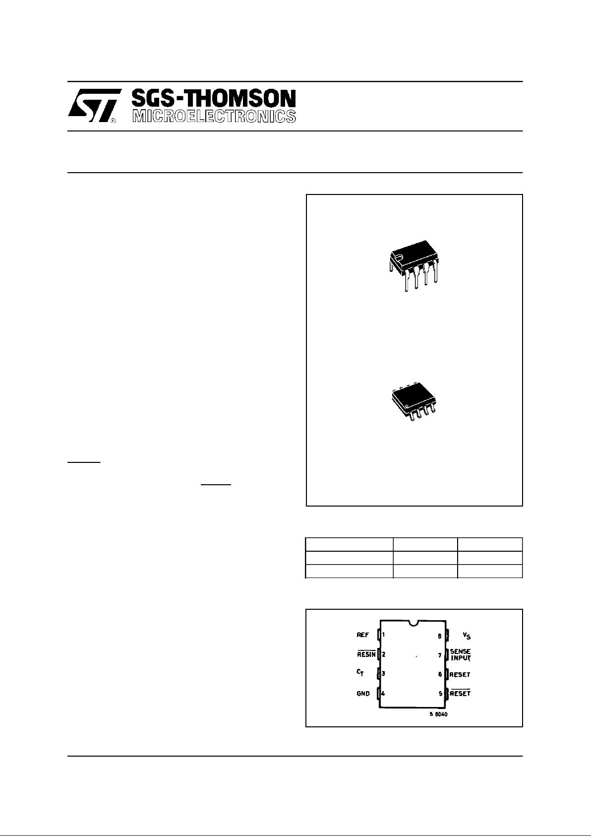
N
Minidip
DESCRIPTION
TheTL7700Aseriesaremonolithicintegratedcircuit
supplyvoltagesupervisorsspecificallydesi-gnedfor
use as reset controllers in microcomputer and microprocessorsystems.During power-upthedevice
teststhesupplyvoltageand keepsthe RESETand
RESEToutputsactive (high and low, respectively)
as long as the supply voltage has not reached its
nominalvoltage value. Taking RESIN low has the
sameeffect.Toensurethatthemicrocomputersystemhasreset,theTL7700Athen initiatesaninternal
timedelaythatdelaysthereturnof the resetoutputs
totheirinactivestates.Sincethetimedelayformost
microcomputersandmicroprocessorsis in theorder
of severalmachinecycles,the device internaltime
delayis determinedby anexternaltimedelayisdeterminedby an externalcapacitorconnectedto the
C
T
input(pin3).
t
d
=1.3 x 10⁴xC
T
Where: CTisin farads(F) and tdinseconds(s).In
addition,when thesupply voltagedrops below the
nominal value, the outputs will be active until the
supplyvoltagereturns to thenominalvalue.An externalcapacitor(typically0.1µF)mustbeconnected
to theREF output(pin1) to reducethe influenceof
fasttransientsin thesupply voltage.
TheTL7700AIseriesis characterized for operation
from– 25
o
Cto85oC ;theTL7700ACseriesis char-
acterizedfrom 0
o
Cto70oC.
D
SO8
ORDERINGNUMBERS
Temperature Range Minidip S08
0to70
o
C TL77XXACP TL77XXACD
-25to 85
o
C TL77XXAIP TL77XXAID
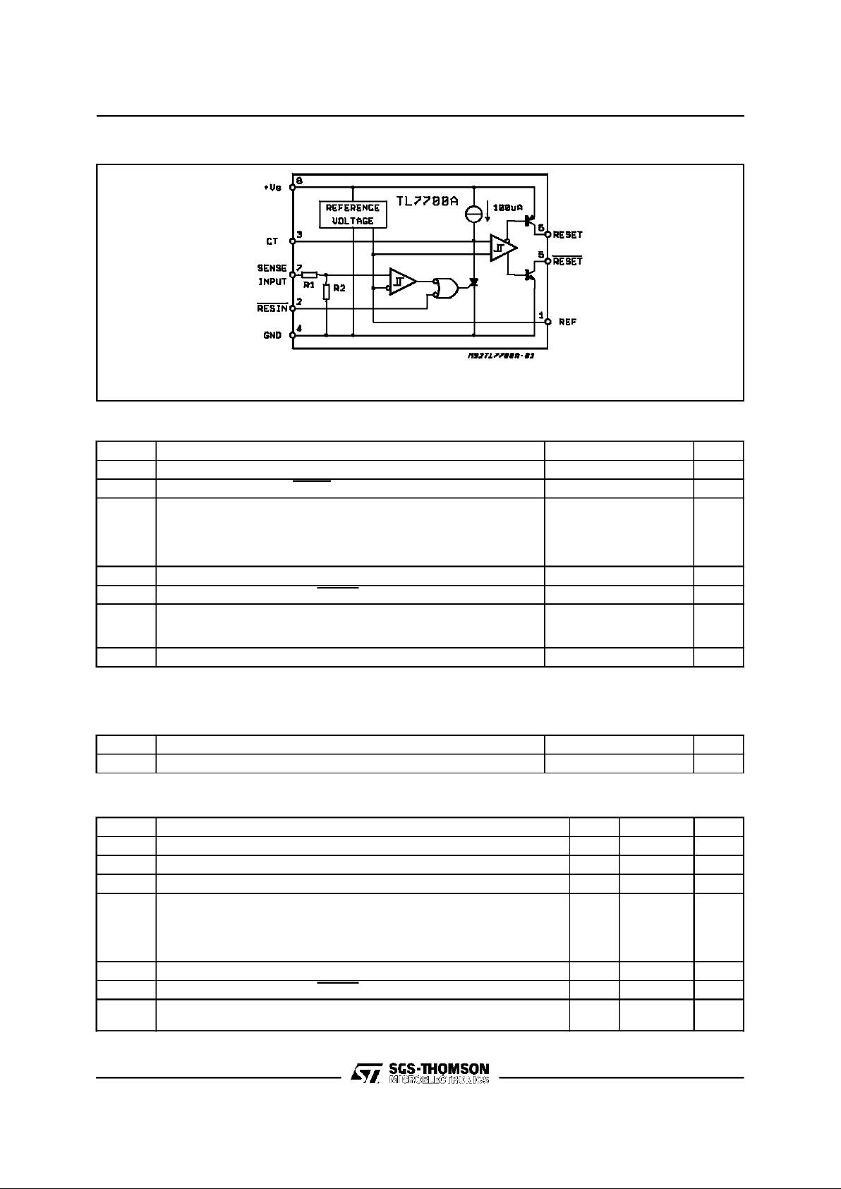
PIN CONNE C TI ON (top view)
1/7
*
TL7702A R1 =0Ω, R2 = open ; TL7705A R1 = 7.8KΩ, R2 = 10kΩ;TL7709A R1 = 19.7KΩ,R2 = 10kΩ;
TL7712A R1 = 32.7kΩ, R2 = 10kΩ; TL7715AR1= 43.4KΩ, R2 = 10kΩ.
BLOCK DIAGRAM
ABSOLUTE MAXIMUM RATINGS
Symbol Parameter Value Unit
V
S
Supply Voltage, VCC- (see note 1) 20 V
V
i
Input Voltage Range at RESIN -0.3 to 20 V
V
i
Input Voltage at SENSE : TL7702A (see note 2)
TL7705A
TL7709A
TL7712A
TL7715A
-0.3 to 6
-0.3 to 10
-0.3 to 15
-0.3 to 20
-0.3 to 20
V
I
OH
High-level Output Current at RESET -30 mA
I
OL
Low-level Output Current at RESET 30 mA
T
amb
Operating Free-air Temperature Range :
TL77XXAI
TL77XXAC
-25 to 85
0to70
o
C
T
stg
Storage Temperature Range -65 to 150
o
C
Notes: 1. All voltage values are withrespect to thenetwork ground terminal
2. For the TL7700A, the voltage appliedto theSENSEterminalmust never exceed V
s
.
THERMAL DATA
Symbol Parameter Value Unit
R
th j-amb
Thermal Resistance Junction-ambient Max. 120
o
C/W
RECOMMENDED OPERATING CONDITIONS
Symbol Parameter Min. Max. Unit
V
S
Supply Voltage 3.6 18 V
V
IH
High-level Input Voltage at RESIN 2 V
V
IL
Low-level Input Voltage at RESIN 0.6 V
V
i
Voltage at Sense Input TL7702A
TL7705A
TL7709A
TL7712A
TL7715A
0
0
0
0
0
See note 3
10
15
20
20
V
I
OH
High-level Output Current at RESET -16 mA
I
OL
Low-level Output Current at RESET 16 mA
T
amb
Operating Free-air Temperature Range TL77-AI
TL77-AC
-25
0
85
70
o
C
Note : 3. For properoperationof theTL7702A, the voltageapplied to the SENSEterminal should not exceed Vs- 1V or 6V, which everis less.
TL7700A Series
2/7
ELECTRICAL CHARACTERISTICS these specificationsunless otherwise specified, apply for :
T
amb
= –25 to 85oC (TLXXAI),T
amb
= 0 to 70oC (TL77XXAC)
Symbol Parameter Test Conditions (1) Min. Typ. Max. Unit
V
OH
High-level Output Voltage at RESET IOH= –16mA Vs-
1.5
V
V
OL
Low-Level Output Voltage at RESET IOL= 16mA 0.4 V
V
ref
Reference Voltage T
amb
=25oC 2.48 2.53 2.58 V
V
T
Threshold Voltage at SENSE Input TL7702A
TL7705A
TL7709A
TL7712A
TL7715A
V
s
= 3.6V to 18V
T
amb
=25oC
2.48
4.5
7.5
10.6
13.2
2.53
4.55
7.6
10.8
13.5
2.58
4.6
7.7
11
13.8
V
V
T
Threshold Voltage at SENSE Inpu TL7702A
TL7705A
TL7709A
TL7712A
TL7715At
V
s
= 3.6V to 18V 2.45
4.45
7.4
10.4
13
2.53
4.55
7.6
10.8
13.5
2.58
4.6
7.7
11
13.8
V
V
T+,VT–
Hysteresis (2) at SENSE Input TL7702A
TL7705A
TL7709A
TL7712A
TL7715A
V
s
= 3.6V to 18V
T
amb
=25oC
10
15
20
35
45
mV
I
I
Input Current at RESIN Input Vi= 2.4V to V
S
Vi= 0.4V
20
-100
µ
A
I
I
Input Current at SENSE Input TL7702A V
ref<Vi<Vs
- 1.5V 0.5 2
µ
A
I
OH
High-level Output Current at RESET VO= 18V 50 µA
I
OL
Low-level Output Current at RESET VO=0V -50
µ
A
I
S
Supply Current All Inputs and out.
open
1.8 3.3 mA
Notes:
1. All characteristicsare measured withC = 0.1µF from Pin 1 to GND,and with C = 0.1µF fromPin 3 to GND.
2. Hysteresis isthe differencebetween the positivegoinginput threshold voltage.V
T+
,and the negative going input threshold
voltage, V
T-
.
SWITCHING CHARACTERISTICS
Symbol Parameter Test Conditions Min. Typ. Max. Unit
t
pi
Pulse Width at SENSE Input Vih=V
ityp
+0.04 x V
i
ViL=V
ityp
–0.04 x V
i
0.9
µ
s
t
pi
Pulse Width at RESIN Input 0.4
µ
s
t
po
Pulse Width at Output CT= 0.1µF 0.65 1.3 2.6 ms
t
pdHL
Propagation Delay Time from RESIN
to RESET
CL= 100pF, Vs= 5V, RL= 4.7k
Ω
1
µ
s
t
r/f
Rise/Falltime at RESET and RESET CL= 10pF, Vs= 5V, RL= 4.7k
Ω
1
µ
s
TL7700A Series
3/7
 Loading...