

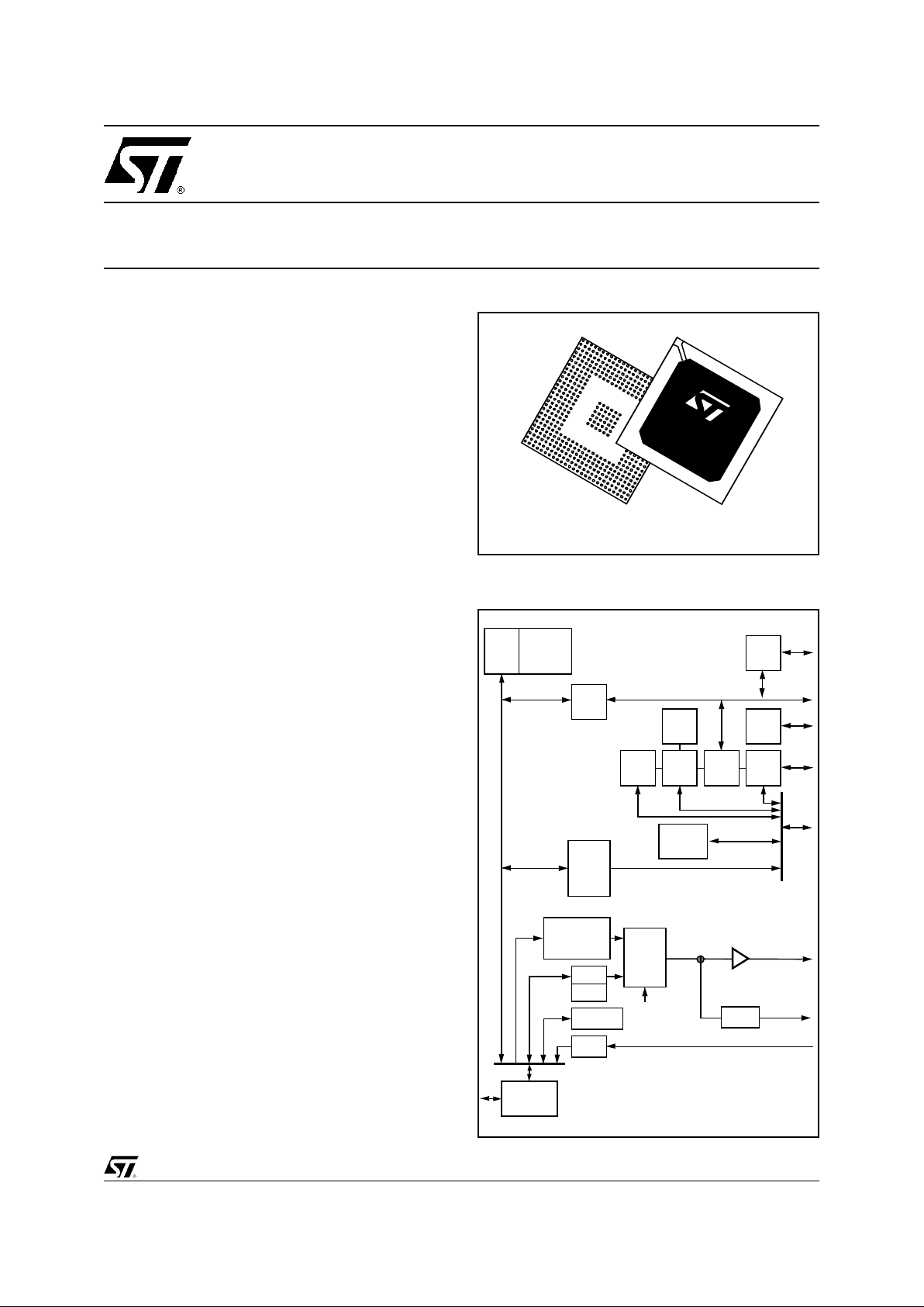
STPC® ATLAS
X86 Core PC Compatible System-on-Chip for Terminals
Issue 1.0 - July 24, 2002 1/111
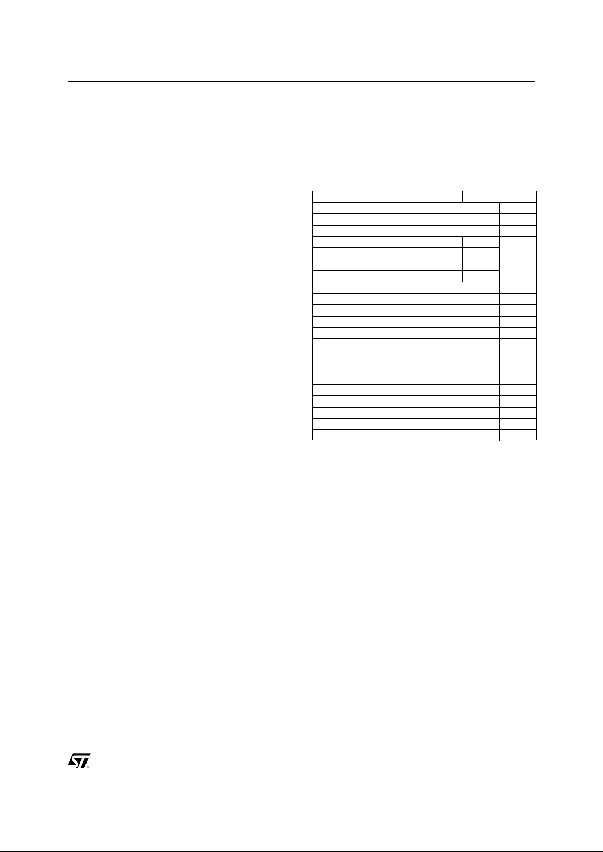
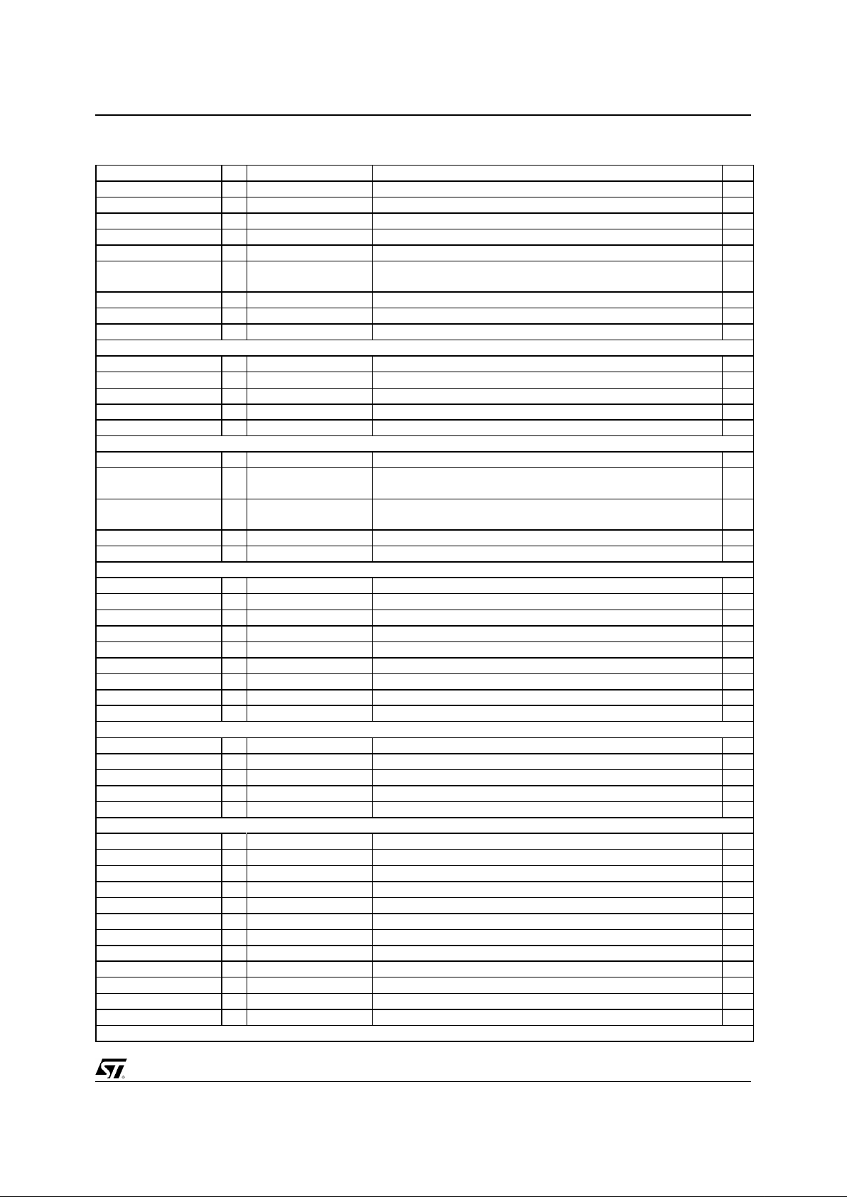
Figure 0-1. Logic Diagram
■
POWERFUL x86 PROCESSOR
■
64-BIT SDRAM UMA CONTROLLER
■
GRAPHICS CONTROLLER
- VGA & SVGA CRT CONTROLLER
- 135MHz RAMDAC
- ENHANCED 2D GRAPHICS ENGINE
■
VIDEO INPUT PORT
■
VIDEO PIPELINE
- UP-SCALER
- VIDEO COLOUR SPACE CONVERTER
- CHROMA & COLOUR KEY SUPPORT
■
TFT DISPLAY CONTROLLER
■
PCI 2.1 MASTER / SLAVE / ARBITER
■
ISA MASTER / SLAVE CONTROLLER
■
16-BIT LOCAL BUS INTERFACE
■
PCMCIA INTERFACE CONTROLLER
■
EIDE CONTROLLER
■
2 USB HOST HU B INTER FACES
■
I/O FEATURES
- PC/AT+ KEYBOARD CONTR O L LER
- PS/2 MOUSE CONTROLLER
- 2 SERIAL PORTS
- 1 PARALLEL PORT
- 16 GENERAL PURPOSE I/Os
- I²C IN TERFACE
■
INTEGRATED PERIPHERAL CONTROLLER
- DMA CONTROLLER
- INTERRUPT CONTROLLER
- TIMER / COUNTERS
■
POWER MANAGEMENT UNIT
■
WATCHDOG
■
JTAG IEEE1149.1
PBGA516
S
T
P
C
A
t
l
a
s
x86
Core
Host
I/F
SDRAM
CTRL
SVGA
GE I/F
VIP
PCI
m/s
LB
ctrl
PCI Bus
ISA
m/s
IPC
PCI
m/s
ISA Bus
CRTC
Cursor
Monitor
IDE
I/F
PMU
wdog
Video
Pipeline
C Key
K Key
LUT
Local Bus
PCMCIA
I/Os
USB
TFT
TFT I/F
Video In

STPC® ATLAS
2/111
Issue 1.0 - Jul
y
24, 2002
DESCRIPTION
The STPC Atlas integrates a standard 5th
generation x86 core along with a powerful UMA
graphics/video chipset, support logic including
PCI, ISA, Local Bus, USB, EIDE controllers and
combines them with standard I/O interfaces to
provide a single PC compatible subsystem o n a
single device, suitable for all kinds of terminal and
industrial appliances.
■
X86 Processor core
■
Fully static 32-bit 5-stage pipeline, x86
processor fully PC compatib l e .
■
Can access up to 4GB of external memory.
■
8Kbyte unified instruction and data cache
with write back and write through capability.
■
Parallel processing integral floating point unit,
with automatic power down.
■
Runs up to 133 MHz (X2).
■
Fully static design for dynamic clock control.
■
Low power and system management modes.
■
Optimized design for 2.5V operation.
■
SDRAM Controller
■
64-bit data bus.
■
Up to 90MHz SDRAM clock speed.
■
Integrated system memory, graphic frame
memory and video frame memory.
■
Supports 8MB up to 128 MB system memory .
■
Supports 16-Mbit, 64-Mbit and 128-Mbit
SDRAMs.
■
Support s 8, 16, 32, 64, and 128 MB DIMMs.
■
Supports buffered, non buffered, and
registered DIMMs
■
4-line write buffers f or CPU to DRAM and PCI
to DRAM cycles.
■
4-line read prefetch buffers for PCI masters.
■
Programmable latency
■
Programmable timing for SDRAM
parameters.
■
Support s -8, -10, -12, -13, -15 memory par t s
■
Supports memory hole between 1MB and
8MB for PCI/ISA busses.
■
32-bit access, Autoprecharge & Power-down
are not supported.
■
Enhanced 2D Graphics Controller
■
Support s pixel depths of 8, 16, 24 and 32 bit.
■
Full BitBLT implementat ion for all 256 raster
operations defined for Windows.
■
Support s 4 transparent BLT modes - Bitmap
Transparency, Pat tern Transparency, Source
Transparency and Destination Transparency.
■
Hardware clipping
■
Fast line draw engin e with anti-aliasing.
■
Supports 4-bit alpha blended font for anti-
aliased text display.
■
Complete double buffered registers for
pipelined operation.
■
64-bit wide pipelined architecture running at
90 MHz. Hardware clipping
■
CRT Controlle r
■
Integrated 135MHz triple RAMDAC allowing
for 1280 x 1024 x 75Hz display.
■
8-, 16-, 24-bit pixels.
■
Interlaced or non-interlaced output.
■
Video Input port
■
Accepts video inputs in CCIR 601/656 mode.
■
Optional 2:1 decimator
■
Stores captured video in off setting area of
the onboard frame buffer.
■
HSYNC and B/T generation or lock onto
external video timing source.
■
Video Pipeli ne
■
Two-tap interpolative horizontal filter.
■
Two-tap interpolative vertical filter.
■
Color space conversion (RGB to YUV and
YUV to RGB).
■
Programmable window size.
■
Chroma and color keying for integrat ed video
overlay.

STPC® ATLAS
Issue 1.0 - July 24, 2002 3/111
■
TFT Int erface
■
Programmable panel size up to 1024 by 1024
pixels.
■
Support for VGA and SVGA active matrix
TFT flat panels with 9, 12, 18-bit interface (1
pixel per clock).
■
Support for XGA and SXGA active matrix
TFT flat panels with 2 x 9-bit interface (2
pixels per clock).
■
Programmable image positionning.
■
Programmable blank space insertion in text
mode.
■
Programmable horizontal a nd vertical image
expansion in graphic mode.
■
One fully programmable PWM (Pulse Width
Modulator) signals to adjust the flat panel
brightness and contrast.
■
Support s
PanelLink
TM
high speed serial
transmitter externally for high resolution
panel interface.
■
PCI Controller
■
Compatible with PCI 2.1 specification.
■
Integrated PCI arbitration interface. Up to 3
masters can connect directly. External logic
allows for greater than 3 masters.
■
Translation of PCI cycles to ISA bus.
■
Translation of ISA maste r initiated cycle to
PCI.
■
Support for burst read/write from PCI master.
■
PCI clock is 1/2, 1/3 or 1/4 Host bus clock.
■
ISA master/slave
■
Generates the ISA clock from either
14.318 MH z o s c illator clock or P CI c lo ck
■
Support s programmable extra wait state for
ISA cycles
■
Supports I/O recovery time for back to back
I/O cycles.
■
Fast Gate A20 and Fast reset.
■
Support s the single ROM that C, D, or E.
blocks shares with F block BIOS ROM.
■
Support s flash ROM.
■
Support s ISA hidden re fresh.
■
Buffered DMA & ISA master cycl es t o reduce
bandwidth utilization of the PCI and Host
bus.
■
Local Bus interface
■
Multiplexed with ISA/DMA interface.
■
Low latency asynchronous bus
■
16-bit data bus with word steering capability.
■
Programmable timing (Host clock granularity)
■
4 Programmable Flash Chip Select.
■
8 Programmable I/O Chip Select.
■
I/O devic e timi n g (set u p & reco very time)
programmable
■
Support s 32-bit Flash burst.
■
2-level hardware ke y protection for Flash boot
block protection.
■
Supports 2 banks of 32MB flash devices with
boot block shadowed to 0x000F0000.
■
Reallocatable Memory space Windows
■
EIDE Interface
■
Supports PIO
■
Transfer Rates to 22 MBytes/sec
■
Supports up to 4 IDE devices
■
Concurrent channel operation (PIO modes) -
4 x 32-Bit Buffer FIFOs per channel
■
Support for PIO mode 3 & 4.
■
Individual drive timing for all four IDE devices
■
Support s both legacy & native IDE modes
■
Supports hard drives larger than 528MB
■
Support for CD-ROM and tape peripherals
■
Backward compatibil it y wit h ID E (ATA-1).
■
Integrated Peripheral Controller
■
2X8237/AT compatible 7-channel DMA
controller.
■
2X8259/AT compatible interrupt Controller.
16 interrupt inputs - ISA and PCI.
■
Three 8254 compatible Timer/Counters.
■
Co-processor error support logic.
■
Support s external RTC (Not in Local Bus
Mode).

STPC® ATLAS
4/111
Issue 1.0 - Jul
y
24, 2002
■
PCMCIA interface
■
Support one PCMCIA 68-pin standard PC
Card Socket .
■
Power Management support.
■
Support PCMCIA/ATA specifications.
■
Support I/O PC Card with pulse-mode
interrupts.
■
USB Interface
■
USB 1.1 compatible.
■
Open HCI 1.0 compliant.
■
User configurable RootHub.
■
Support for both LowSpeed and HighSpeed
USB devices.
■
No bi-directionnal or Tri-state busses.
■
No level sensitive lat ches.
■
System Management Interrupt pin support
■
Hooks for legacy device support.
■
Keyboard interface
■
Fully PC/AT+ compatible
■
Mouse interface
■
Fully PS/ 2 compatible
■
Serial inte rface
■
15540 compatible
■
Programmable word length, stop bits, parity.
■
16-bit programmable baud rate generator.
■
Interrupt generator.
■
Loop-back mode.
■
8-bit scratch register.
■
Two 16-bit FIFOs.
■
Two DMA handshake lines.
Paralle l port
■
All IEEE Standard 1284 protocols supported:
Compatibility, Nibble, Byte, EPP, and ECP
modes.
■
16 bytes FIFO for ECP.
■
Power Manage me nt
■
Four power saving modes: On, Doze,
Standby, Suspend.
■
Programmable system activity detector
■
Support s Intel & Cyrix SMM and APM.
■
Supports STOPCLK.
■
Support s IO trap & restart .
■
Independent peripheral time-out timer to
monitor hard disk, serial & parallel port.
■
128K SM_RAM address space from
0xA0000 to 0xB0000
■
JTAG
■
Boundary Scan com patible IEEE1149 .1.
■
Scan Chain control.
■
Bypass register compatible IEEE1149.1.
■
ID register compatible IEEE1149.1.
■
RAM BIST co ntrol.
.
ExCA
is a trademark of PCMCIA / JEIDA.
PanelLink
is a trademark of SiliconImage, Inc

GENERAL DESCRIPTION
Issue 1.0 - July 24, 2002 5/111
1. GENERAL DESCRIPTIO N
At the heart of the STPC Atlas is an advanced
processor block that includes a powerful x86
processor core along with a 64-bit SDRAM
controller, advanced 64-bit accelerated graphics
and video controller, a high speed PCI bus
controller and industry standard PC chip set
functions (Interrupt controller, DMA Controller,
Interval timer and ISA bus).
The STPC Atlas has in addition, a TFT output, a
Video Input, an EIDE controller, a Local Bus
interface, PCMCIA and super I/O features
including USB host hub.
1.1. ARCHITECTURE
The STPC Atlas ma ke s use of a tightly coupled
Unified Memory Architecture (UMA), where the
same memory array is used for CPU main
memory and graphics frame-buf fer. This me ans a
reduction in total system memory for system
performances that are equal to that of a
comparable frame buffer and system memory
based system, and generally much better, due to
the higher memory bandwidth allowed by
attaching the graphics engine directly to the 64-bit
processor host interface runni ng at the speed of
the processor bus rather than the traditional PCI
bus.
The 64-bit wide memory array provides the
system with an 800MB/s peak bandwidth. This
allows for higher resolution screens and greater
color depth. The processor bus runs a t 133 MHz,
further increasing “standard” bandwidth by at least
a factor of two.
The ‘standard’ PC chipset functions (DMA,
interrupt controller, timers, power management
logic) are integrated together with the x86
processor core; additional low bandwidth
functions such as communication ports are
accessed by the ST PC Atlas via an internal ISA
bus.
The PCI bus is the ma in data comm unication link
to the STPC A tl as c hip. Th e STPC Atl as t ran slate s
appropriate host bus I/O an d M em ory cycles onto
the PCI bus. It also supports the generation of
Configuration cycles on the PCI bus. The STPC
Atlas, as a PCI bus agent (host bridge class), is
compatible with PCI specification 2.1. The chipset also implements the PCI mandatory header
registers in Type 0 PCI configuration space for
easy porting of PCI aware system BIOS. The
device contains a PCI arbitration function for three
external PCI devi ces.
Figure 1-1 describes this architecture.
1.2. GRAPHICS FEATURES
Graphics functions are controlle d through t he onchip SVGA controller and the monitor display is
produced through the 2D graphics display engine.
This Graphics Engine is tuned to work with the
host CPU to provide a balanced graphics system
with a low silicon area cost. It performs limited
graphics drawing operations which include
hardware acceleration of t ext, bitblts, transparent
blts and fills. The results of these operations
change the contents of the on-screen or offscreen frame buffer areas of SDRAM memory.
The frame buffer can occupy a space up to 4
Mbytes anywhere in the physical main memory.
The maximum graphics resolution supported is
1280 x 1024 in 16 Million colours at 75 Hz refresh
rate and is VGA and SVGA compatible. Horizontal
timing fields are VGA compatible while the vertical
fields are extended by one bit to accommodate
above display resolution.
To generate the TFT output, the STPC Atlas
extracts the digital video stream before the
RAMDAC and reformats i t to the TF T form at. T he
height and width of the flat panel are
programmable.
1.3. INTERFACES
An industry standard EIDE (ATA 2) controller is
built in to the STPC Atlas and connected internally
via the PCI bus.
The STPC Atlas integrates two USB ports.
Universal Serial Bus (USB) is a general purpose
communications interface for connecting
peripherals to a PC. The USB Open Host
Controller Interface (Open HCI) Specification,
revision 1.1, supports speeds of up to 12 MB/s.
USB is royalty free and is likely to replace lowspeed legacy serial, parallel, keyboard, mouse
and floppy drive interfaces. USB Revision 1.1 is
fully supported under Microsoft W indows 98 and
Windows 2000.
The STPC Atlas PCMCIA controller has been
specifically designed to provide the interface with
PCMCIA cards which cont ain additional memory
or I/O
The power management control facilities include
socket power control, insertion/removal capability,
power saving with Windows inactivity, NCS
controlled Chip Power Down, together with further
controls for 3.3V suspend with Modem Ring
Resume Detection.

GENERAL DESCRIPTION
6/111
Issue 1.0 - Jul
y
24, 2002
The STPC Atlas implements a multi-function
parallel port. The standard PC/AT compatible
logical address assignments for LPT1, LPT2 and
LPT3 are supported. It can be configured for any
of the following three modes and supports the
IEEE Standard 1284 parallel interface protocol
standards, as follows:
- Compatibility Mode (Forward channel, standard)
- Nibble Mode (Reverse channel, PC compatible)
- Byte Mode (Reverse channel, PS/2 compatible)
The General Purpose Input/Output (GPIO)
interface provides a 16-bit I/O facility, using 16
dedicated device pins. It is organised using two
blocks of 8-bit Registers, one for lines 0 to 7, the
other for lines 8 to 15.
Each GPIO port can be configured as an input or
an output simply by programming the assoc iated
port direction control register. All GPIO ports are
configured as inputs at reset, which also la tches
the input levels into the Strap Registers. The input
states of the ports are thus recorded automatically at reset, and this can be used as a strap
register anywhere in the system.
1.4. FEATURE MULTIPLEXING
The STPC Atlas BGA package has 516 balls. This
however is not sufficient for all of the integrat ed
functions available; some features therefore share
the same balls and cannot thus be used at the
same time. The ST PC A tlas c onfigurat ion is d one
by ‘strap options’. This is a set of pull-up or pulldown resistors on the memory data bus, checked
on reset, which auto-configure the STPC Atlas.
There 3 multiplexed functions are the external ISA
bus, the Local Bus and the PCMCIA interface.
1.5. POWER MANAGEMENT
The STPC Atlas core is compliant with the
Advanced Power Management (APM)
specification to provide a standard method by
which the BIOS can control the power used by
personal computers. The Power Management
Unit (PMU) module controls the power
consumption, providing a comprehensive set of
features that controls the power usage and
supports compliance with the United States
Environmental Protection Agency's Energy Star
Computer Program. The PMU provides the
following hardware structures to assist the
software in managing the system power
consumption:
- System Activity Detection.
- 3 power-down timers detecting system inactivity:
- Doze timer (short durations).
- Stand-by timer (medium durations).
- Suspend timer (long durations).
- House-keeping activity detection.
- House-keeping timer to cope with short bursts of
house-keeping activity while dozing or in stand-by
state.
- Peripheral activity detection.
- Peripheral timer detecting peripheral inactivity
- SUSP# modulation to adjust the system
performance in various power down state s of the
system including full power-on state.
- Power control outputs to disable power from
different planes of the board.
Lack of system activity for progressively longer
periods of time is detected by the three power
down timers. These timers can generate SMI
interrupts to CPU so that the SMM software can
put the system in decreasing states of power
consumption. Alternatively, system activity in a
power down state can g enerate an SMI interrupt
to allow the software to bring the system back up
to full power-on state. The chip-set supports up to
three power down states described above; these
correspond to decreasing levels of power savings.
Power down puts the STPC Atlas into suspend
mode. The processor completes execution of the
current instruction, any pending decoded
instructions and associated bus cycles. During the
suspend mode, internal clocks are stopped.
Removing power-down, the processor resumes
instruction fetching and begins execution in the
instruction stream at the point it had stopped.
Because of the static nature of the core, no
internal data is lost.
1.6. JTAG
JTAG stands for Joint Test Action Group and is
the popular name for IEEE Std. 1149.1, Standard
Test Access Port and Boundary -S can Architec ture. This built-in circuitry is used to assist in the
test, maintenance and support of functional circuit
blocks. The circuitry includes a standard interface
through which instructions and test data are
communicated. A set of test features is defined,
including a boundary-scan registe r so that a
component is able to respond to a minimum set of
test instructions.

GENERAL DESCRIPTION
Issue 1.0 - July 24, 2002 7/111
Figure 1-1. Functional description.
x86
Core
Host
I/F
SDRAM
CTRL
SVGA
GE I/F
VIP
PCI
m/s
LB
CTRL
PCI Bus
ISA
m/s
IPC
PCI
m/s
ISA Bus
CRTC
Cursor
Monitor
IDE
I/F
PMU
Video
Pipeline
C Key
K Key
LUT
Local Bus
PCMCIA
I/Os
USB
TFT
TFT I/F
Video In
JTAG

GENERAL DESCRIPTION
8/111
Issue 1.0 - Jul
y
24, 2002
1.7. CLOCK TREE
The STPC Atlas integrates many features and
generates all its clocks from a single 14MHz
oscillator. This results in multiple clock domains as
described in Figure 1-2.
The speed of the PLLs is either fixed (DE VCLK),
either programmable by strap option (HCLK)
either programmable by software (DCLK, MCLK).
When in synchronized mode, MCLK speed is fixed
to HCLKO speed and HCLKI is generated from
MCLKI.
Figure 1-2. STPC Atlas clock architecture
Kbd/Mouse
IPC
SDRAM controller
North Bridge
14.31818 MHz
XTALO XTALI
OSC14M ISACLK
1/4
DEVCLK
DEVCLK
(24MHz)
PLL
(14MHz)
1/2
UARTs
HCLK
PLL
PCICLKI PCICLKO
South Bridge
PWM
1/2
1/3
HCLK
DCLK
PLL
MCLK
PLL
DCLK
MCLKIMCLKO
USB
CRTC,Video,TFT
CPU
x2
VCLK
48MHz
// Port
1/4
1/2
1/26
1/6
VIP
GE, LDE, AFE
PCMCIA
Local Bus
Host
ISA
HCLKI
HCLKO

GENERAL DESCRIPTION
Issue 1.0 - July 24, 2002 9/111
Figure 1-3. Typical ISA-based Application.
Flash
Boot
ISA
PCI
EIDE
2 Serial Ports
Parallel Port
SVGA
TFT
IRQ
DMA.REQ
DMA.ACK
STPC Atlas
Mouse
Keyboard
USB
VIP
RTC
SDRAM
16 GPIOs
ROMCS#
5V tolerant

GENERAL DESCRIPTION
10/111
Issue 1.0 - Jul
y
24, 2002
Figure 1-4. Typical PCMCIA-based Application.
PCI
Flash
EIDE
2 Serial Ports
Parallel Port
SVGA
TFT
STPC Atlas
Mouse
Keyboard
USB
Boot
VIP
SDRAM
16 GPIOs
ROMCS#
PCMCIA
5V tolerant

GENERAL DESCRIPTION
Issue 1.0 - July 24, 2002 11/111
Figure 1-5. Typical Local-Bus-based Application.
Flash
Boot
PCI
STPC Atlas
RTC
EIDE
2 Serial Ports
Parallel Port
SVGA
TFT
Mouse
Keyboard
USB
VIP
SDRAM
16 GPIOs
IRQ
Local Bus

GENERAL DESCRIPTION
12/111
Issue 1.0 - Jul
y
24, 2002
PIN DESCRIPTION
Issue 1.0 - July 24, 2002 13/111
2. PIN DESCRIPTION
2.1. INTRODUCTION
The STPC Atlas integrates most of the
functionalities of the PC architecture. Therefore,
many of the traditional interconnections between
the host PC microprocessor and the peripheral
devices are totally internal to the STPC Atlas. This
offers improved performance due to the tight
coupling of the processor core and it’s peripherals.
As a result many of the external pin connections
are made directly to the on-chip peripheral
functions.
Table 2-1 describes the physical implement ation
listing signal types a nd their functional ities. Tab le
2-2 provides a full pin listing and description.
Table 2-6 provides a full l isting of the STP C A t las
package pin location physical connection. Please
refer to the pin allocation drawing for reference.
Due to the number of pins available for the
package, and the number of functional I/Os, some
pins have several functions, selectable by strap
option on Reset. Table 2-4 provides a summary of
these pins and their functions.
Non multi-functional pins associated with a
particular function are not available for use
elsewhere when that function is disabled. For
example, when in the ISA mode, the Local Bus is
disabled totally and Local Bus pins are set to the
tri-state (high-impedance) condition.
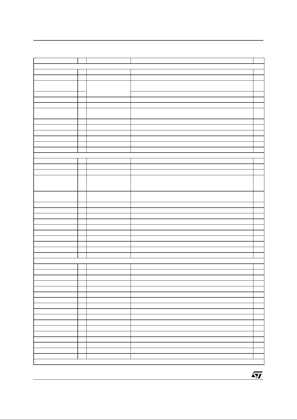
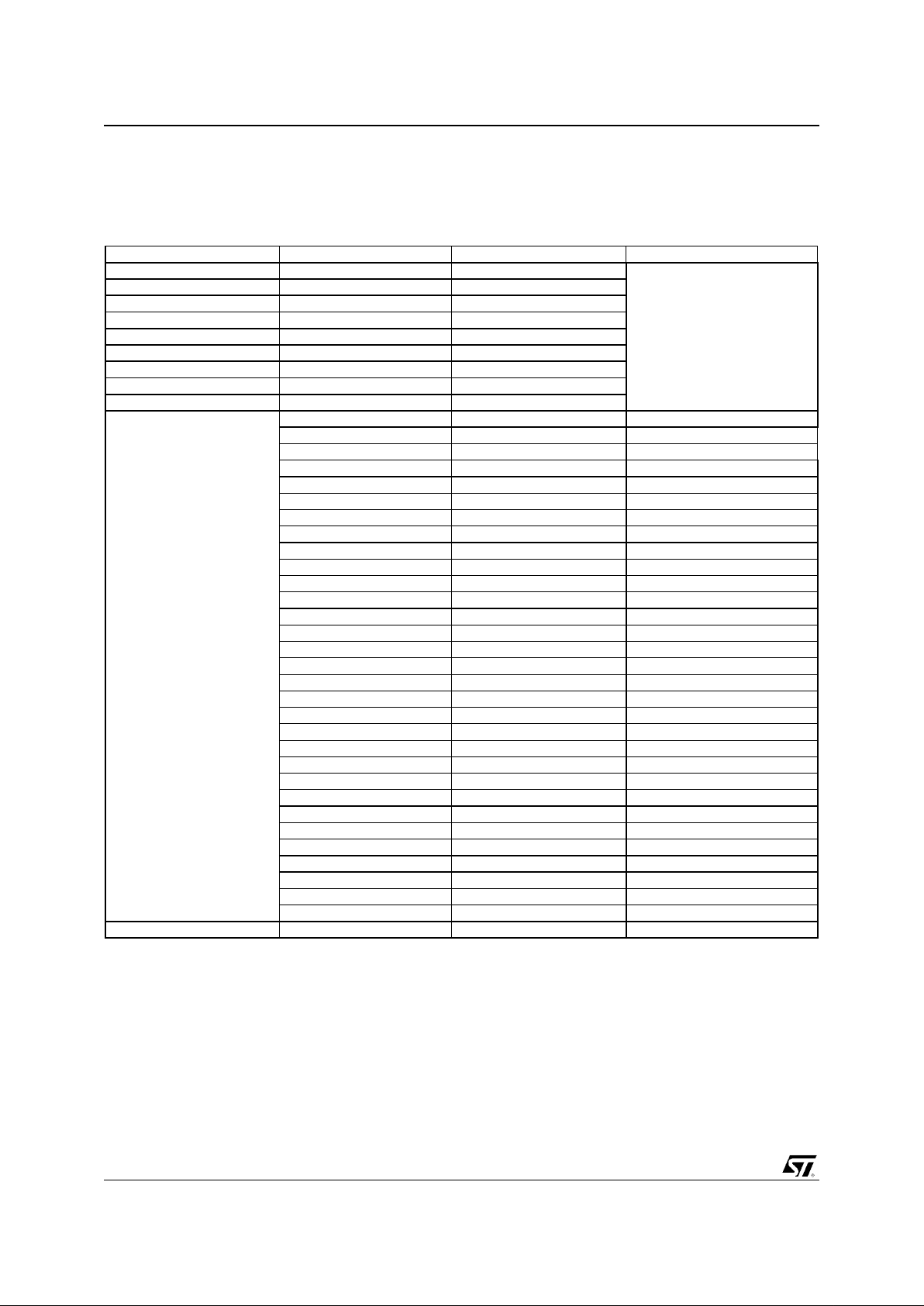
Table 2-1.
Signal Description
Group name Qty
Basic Clocks, Reset & Xtal (SYS) 19
SDRAM Controller (SDRAM) 95
PCI Controller 51
ISA Controller 80
100
Local Bus I/F 67
PCMCIA Controller 62
IDE Controller 34
VGA Controller (VGA) / I
2
C10
Video Input Port 11
TFT output 24
USB Controller 6
Serial Interface 16
Keyboard/Mouse Controller 4
Parallel Port 18
GPIO Signals 16
JTAG Signals 5
Miscellaneous 5
Grounds 96
V
DD
3.3 V/2.5 V 36
Reserved 4
Total Pin Count 516
PIN DESCRIPTION
14/111
Issue 1.0 - Jul
y
24, 2002
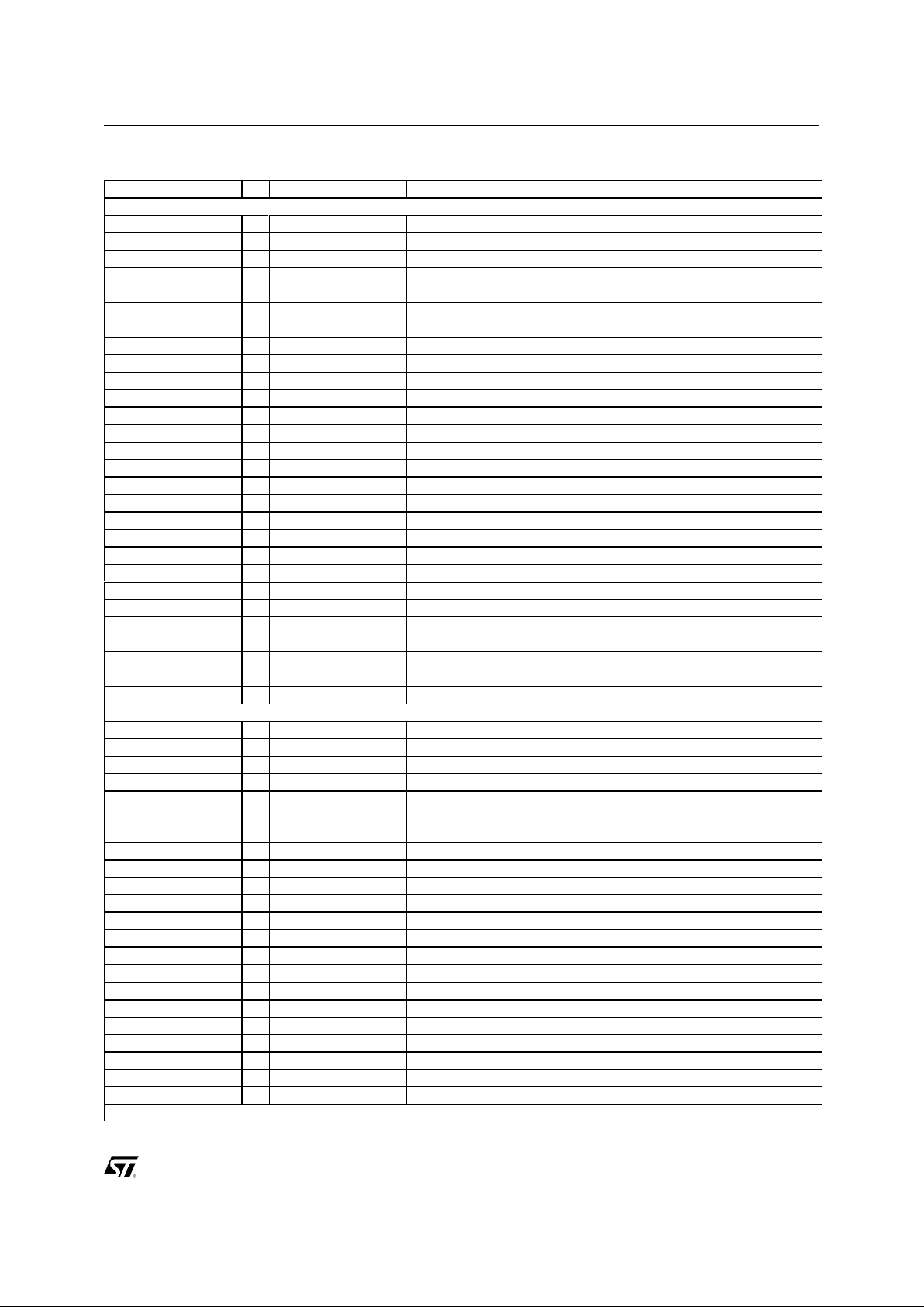
Table 2-2.
Definitio n of Si gn a l Pins
Signal Name Dir Buffer Type
1
Description Qty
BASIC CLOCKS AND RESETS
SYSRSTI# I SCHMITT_FT System Reset / Power good 1
SYSRSTO# O BD8STRP_FT Reset Output to System 1
XTALI I
OSCI13B
14.31818 MHz Crystal Input
External Oscillator Input
1
XTALO O 14.31818 MHz Crystal Output 1
PCI_CLKI I TLCHT_FT 33 MHz PCI Input Clock 1
PCI_CLKO O BT8TRP_TC 33 MHz PCI Output Clock 1
ISA_CLK,
ISA_CLK2X
O BT8TRP_TC
ISA Clock x1 and x2
Multiplexer Select Line for IPC
2
OSC14M O BD8STRP_FT ISA bus synchronisation clock 1
HCLK I/O BD4STRP_FT 66 MHz Host Clock (Test pin) 1
DEV_CLK O BT8TRP_ TC 24 MHz Peripheral Clock 1
DCLK I/O BD4STRP_FT 135 MHz Dot Clock 1
V
DD
_xxx_PLL 2.5V Power Supply for PLL Clocks 7
MEMORY CONTROLLER
MCLKI I TLCHT_TC Memory Clock Input 1
MCLKO O BT8TRP_TC Memory Clock Output 1
CS#[1:0] O BD8STRP_TC DIMM Chip Select 2
CS#[3]/MA[12]/BA[1] O BD16STARUQP_TC
DIMM Chip Select
Memory Address
Bank Address
1
CS#[2]/MA[11] O BD16STARUQP_TC
DIMM Chip Select
Memory Address
1
MA[10:0] O BD16STARUQP_TC Memory Row & Column Address 11
BA[0] O BD16STARUQP_TC Bank Address 1
RAS#[1:0] O BD16STARUQP_TC Row Address Strobe 2
CAS#[1:0] O BD16STARUQP_TC Column Address Strobe 2
MWE# O BD16STARUQP_TC Write Enable 1
MD[0] I/O BD8STRUP_F T Memory Data 1
MD[53:1] I/O BD8TRP_TC Memory Data 53
MD[63:54] I /O BD8STRU P_F T Memory Data 10
DQM[7:0] O BD8STRP_TC Data Input/Ouput Mask 8
PCI INTERFACE
AD[31:0] I/O BD8PCIARP_FT Address / Data 32
CBE[3:0] I/O BD8PCIARP_FT Bus Commands / Byte Enables 4
FRAME# I/O BD8PCIARP_FT Cycle Frame 1
TRDY# I/O BD8PCIARP_FT Target Ready 1
IRDY# I/O BD8PCIARP_FT Initiator Ready 1
STOP# I/O BD8PCIARP_FT Stop Transaction 1
DEVSEL# I/O BD8PCIARP_FT Device Select 1
PAR I/O BD8PCIARP_FT Parity Signal Transactions 1
PERR# I/O BD8PCIARP_FT Parity Error 1
SERR# O BD8PCIARP_FT System Error 1
LOCK# I TLCHT_FT PCI Lock 1
PCI_REQ#[2:0] I BD8PCIARP_FT PCI Request 3
PCI_GNT#[2:0] O BD8PCIARP_FT PCI Grant 3
PCI_INT#[3:0] I BD4STRUP_FT PCI Interrupt Request 4
Note
1
; See
Table 2-3
for buffer type descriptions
PIN DESCRIPTION
Issue 1.0 - July 24, 2002 15/111
ISA BUS INTERFACE
LA[23:17] O BD8STRUP_FT Unlatched Address Bus 7
SA[19:0] O BD8STRUP_FT Latched Address Bus 20
SD[15:0] I/O BD8STRP_FT Data Bus 16
IOCHRDY I BD8STRUP_FT I/O Channel Ready 1
ALE O BD4STRP_FT Address Latch Enable 1
BHE# O BD8STRUP_FT System Bus High Enable 1
MEMR#, MEMW# I/O BD8STRUP_FT Memory Read & Write 2
SMEMR#, SMEMW# O BD8STRP_FT System Memory Read and Write 2
IOR#, IOW# I/O BD8STRUP_FT I/O Read and Write 2
MASTER# I BD4STRUP_FT Add On Card Owns Bus 1
MCS16# I BD4STRUP_F T Memory Chip Select 16 1
IOCS16# I BD4STRUP_FT I/O Chip Select 16 1
REF# I BD8STRP _FT Refresh Cycle 1
AEN O BD8STRUP_FT Address Enable 1
IOCHCK# I BD4STRUP_FT I/O Channel Check (ISA) 1
RTCRW# O BD4STRP_FT RTC Read / Write# 1
RTCDS# O BD4STRP_FT RTC Data Strobe 1
RTCAS O BD4STRP_FT RTC Address Strobe 1
RMRTCCS# O BD4STRP_FT ROM / RTC Chip Select 1
GPIOCS# I/O BD4STRP_FT General Purpose Chip Select 1
IRQ_MUX[3:0] I BD4STRP_FT Multiplexed Interrupt Request 4
DACK_ENC[2:0] O BD4STRP_FT DMA Acknowledge 3
DREQ_MUX[1:0] I BD4STRP_FT Multiplexed DMA Request 2
TC O BD4STRP_FT ISA Terminal Count 1
ISAOE# I BD4STRP_FT ISA (0) / IDE (1) SELECTION 1
KBCS# I/O BD4STRP_FT External Keyboard CHIP SELECT 1
ZWS# I BD4STRP_FT ZERO WAIT STATE 1
PCMCIA INTERFAC E
RESET O BD8 STRP _FT Reset 1
A[23:0] O BD8STRUP_FT Address Bus 24
D[15:0] I/O BD8STRP_FT Data Bus 16
IORD#, IOWR# O BD8STRUP_FT I/O Read and Write 2
WP / IOIS16# I BD4STRUP_FT
DMA Request // Write Protect
I/O Size is 16 bit
1
BVD2, BVD1 I BD4STRUP_FT Battery Voltage Detect 2
READY# / IREQ# I BD4STRUP_FT Busy / Ready# // Interrupt Request 1
WAIT# I BD8STRUP_FT Wait 1
OE# O BD8STRUP_FT Output Enable // DMA Terminal Count 1
WE# O BD4STRP_FT Write Enable // DMA Terminal Count 1
REG# O BD4STRUP_FT DMA Acknowledge // Register 1
CD2#, CD1# I BD4STRUP_FT Card Detect 2
CE2#, CE1# O BD4STRP_FT Card Enable 2
VCC5_EN O BD4STRP_FT Power Switch control: 5 V power 1
VCC3_EN O BD8STRP_FT Power Switch control: 3.3 V power 1
VPP_PGM O BD8STRP_FT Power Switch control: Program power 1
VPP_VCC O BD4STRP_FT Power Switch control: VCC power 1
GPI# I BD4STRP _FT General Purpose Input 1
Table 2-2.
Definitio n of Si gn a l Pins
Signal Name Dir Buffer Type
1
Description Qty
Note
1
; See
Table 2-3
for buffer type descriptions

PIN DESCRIPTION
16/111
Issue 1.0 - Jul
y
24, 2002
LOCAL BUS INTERFACE
PA[24:20,15,9:8,3:0] O BD4STRP_FT Address Bus [24:20], [15], [9:8], [3:0] 12
PA[19,11] O BD8STRP_FT Address Bus [19], [11] 2
PA[18:16,14:12,7:4] O BD8STRUP_FT Address Bus [18:16], [14:12], [7:4] 10
PA[10] O BD4STRUP_FT Address Bus [10] 1
PD[15:0] I/O BD8STRP_FT Data Bus [15:0] 16
PRD# O BD4STRUP_FT Memory and I/O Read signal 1
PWR# O BD4STRUP_FT Memory and I/O Write signal 1
PRDY I BD8STRUP_FT Data Ready 1
IOCS#[7:4] O BD4STRUP_FT I/O Chip Select 4
IOCS#[3] O BD4STRP_FT I/O Chip Select 1
IOCS#[2:0] O BD8STRUP_FT I/O Chip Select 3
PBE#[1] O BD8STRP_FT Upper Byte Enable (PD[15:8]) 1
PBE#[0] O BD4STRUP_FT Lower Byte Enable (PD[7:0]) 1
FCS0# O BD4STRP_FT Flash Bank 0 Chip Select 1
FCS1# O BT8TRP_TC Flash Bank 1 Chip Select 1
FCS_0H# O BD8STRP_FT Upper half Bank 0 Flash Chip Select 1
FCS_0L# O BD8STRP_FT Lower half Bank 0 Flash Chip Select 1
FCS_1H# O BD8STRP_FT Upper half Bank 1 Flash Chip Select 1
FCS_1L# O BD8STRP_FT Lower half Bank 1 Flash Chip Select 1
IRQ_MUX[3:0]
1
I/O BD4STRP_FT Muxed Interrupt Lines 4
IDE CONTROLLER
DD[15:12] I/O BD4STRP_FT Data Bus 4
DD[11:0] I/O BD8STRUP_FT Data Bus 12
DA[2:0] O BD8STRUP_FT Address Bus 3
PCS1, PCS3 O BD8STRUP_FT Primary Chip Selects 2
SCS1, SCS3 O BD8STRUP_FT Secondary Chip Selects 2
DIORDY O BD8STRUP_FT Data I/O Ready 1
PIRQ/SIRQ I BD4STRP_FT Primary / Secondary Interrupt Request 2
PDRQ/SDRQ I BD4STRP_FT Primary / Secondary DMA Request 2
PDACK#/SDACK# O BD8STRP_FT Primary / Secondary DMA Acknowledge 2
PDIOR#/SDIOR# O BD8STRUP_FT Primary / Secondary IO Read 2
PDIOW#/SDIOW# O BD8STRP_FT Primary / Secondary IO Write 2
VGA CONTROLLER
RED, GREEN, BLUE O VDDCO Red, Green, Blue 3
VSYNC, HSYNC I/O BD4STRP_FT Vertical & Horizontal Synchronisations 2
VREF_DAC I ANA DAC Voltage reference 1
RSET I ANA Re sistor Set 1
COMP I ANA Compensation 1
COL_SEL O BD4STRP_FT Colour Select 1
I2C INTERFACE
SCL / DDC[1] I/O BD4STRUP_FT I²C Interface - Clock / VGA DDC[1] 1
SDA / DDC[0] I/O BD4STRUP_FT I²C Interface - Data / VGA DDC[0] 1
TFT INTERFACE
TFTR[5:2] O BD4STRP_TC Red 4
TFTR[1:0] O BD4STRP_FT Red 2
TFTG[5:2] O BD4STRP_TC Green 4
,TFTG[1:0] O BD4STRP_FT Green 2
Table 2-2.
Definitio n of Si gn a l Pins
Signal Name Dir Buffer Type
1
Description Qty
Note
1
; See
Table 2-3
for buffer type descriptions
PIN DESCRIPTION
Issue 1.0 - July 24, 2002 17/111
TFTB[5:2] O BD4STRP_TC Blue 4
TFTB[1:0] O BD4STRP_FT Blue 2
TFTLINE O BD8STRP_TC Horizontal Sync 1
TFTFRAME O BD4STRP_TC Vertical Sync 1
TFTDE O BD4STRP_TC Data Enable 1
TFTENVDD,
TFTENVCC
O BD4STRP_TC Enable Vdd & Vcc of flat panel 2
TFTPWM O BD8STRP_TC PWM back-light control 1
TFTDCLK O BT8TRP_TC Dot clock for Flat Panel 1
VIDEO INPUT PORT
VCLK I/O BD8STRP_FT 27-33 MHz Video Input Port Clock 1
VIN[7:0] I BD4STRP_FT Video Input Data Bus 8
ODD_EVEN# I/O BD4STRP_FT Video Input Odd/even Field 1
VCS I/O BD4STRP_FT Video Input Horizontal Sync 1
USB INTERFACE
OC I TLCHTU_TC Over Current Detect 1
USBDPLS[0]
1
USBDMNS[0]
1
I/O USBDS_2V5 Universal Serial Bus Port 0 2
USBDPLS[1]
1
USBDMNS[1]
1
I/O USBDS_2V5 Universal Serial Bus Port 1 2
POWERON
1
O BT4CRP USB power supply lines 1
SERIAL CONTROLL ER
CTS0#, CTS1# I TLCHT_FT Clear to send, MSR[4] status bit 2
DCD0#, DCD1# I TLCHT_FT Data Carrier detect, MSR[7] status bit 2
DSR0#, DSR1# I TLCHT_FT Data set ready, MSR[5] status bit. 2
DTR0#, DTR1# O BD4STRP_TC Data terminal ready, MSR[0] status bit 2
RI0#, RI1# I TLCHT_FT Ring indicator, MSR[6] status bit 2
RTS0#, RTS1# O BD4STRP_TC Request to send, MSR[1] status bit 2
RXD0, RXD1 I TLCHT_FT Receive data, Input Serial Input 2
TXD0, TXD1 O BD4STRP_TC Transmit data, Serial Output 2
KEYBOARD & MOUSE INTERFACE
KBCLK I/O BD4STRP_TC Keyboard Clock Line 1
KBDATA I/O BD4STRP_TC Keyboard Data Line 1
MCLK I/O BD4STRP_TC Mouse Clock Line 1
MDATA I/O BD4STRP_TC Mouse Data Line 1
PARALLEL PORT
PE I BD14STARP_FT Paper End 1
SLCT I BD14STARP_FT SELECT 1
BUSY# I BD14STARP_FT BUSY 1
ERR# I BD14STARP_FT ERROR 1
ACK# I BD14STARP_FT Acknowledge 1
PDIR# O BD14STARP_FT Parallel Device Direction 1
STROBE# O BD14STARP_FT PCS / STROBE# 1
INIT# O BD14STARP_FT INIT 1
AUTOFD# O BD14STARP_FT Automatic Line Feed 1
SLCTIN# O BD14STARP_FT SELECT IN 1
PPD[7:0] I/O BD14STARP_FT Data Bus 8
Table 2-2.
Definitio n of Si gn a l Pins
Signal Name Dir Buffer Type
1
Description Qty
Note
1
; See
Table 2-3
for buffer type descriptions

PIN DESCRIPTION
18/111
Issue 1.0 - Jul
y
24, 2002
GPIO SIGNALS
GPIO[15:0] I /O BD4STRP _FT General Purpose IOs 16
JTAG
TCLK I TLCHT_FT Test Clock 1
TRST I TLCHT_FT Test Reset 1
TDI I TLCHTD_FT Test Data Input
TMS I TLCHT_FT Test Mode Set 1
TDO O BT8TRP_TC Test Data output 1
MISCELLANEOUS
SCAN_ENABLE I TLCHTD_FT Test Pin - Reserved 1
SPKRD O BD4STRP_FT Speaker Device Output 1
Table 2-2.
Definitio n of Si gn a l Pins
Signal Name Dir Buffer Type
1
Description Qty
Note
1
; See
Table 2-3
for buffer type descriptions
Table 2-3.
Buffer Type Descriptions
Buffer Description
ANA Analog pad buffer
OSCI13B Oscillator, 13 MHz, HCMOS
BT4CRP LVTTL Output, 4 mA drive capability, Tri-State Control
BT8TRP_TC LVTTL Output, 8 mA drive capability, Tri-State Control, Schmitt trigger
BD4STRP_FT LVTTL Bi-Directional, 4 mA drive capability, Schmitt trigger, 5V tolerant
BD4STRUP_FT LVTTL Bi-Directional, 4 mA drive capability, Schmitt trigger, Pull-Up, 5V tolerant
BD4STRP_TC LVTTL Bi-Directional, 4 mA drive capability, Schmitt trigger
BD8STRP_FT LVTTL Bi-Directional, 8 mA drive capability, Schmitt trigger, 5V tolerant
BD8STRUP_FT LVTTL Bi-Directional, 8 mA drive capability, Schmitt trigger, Pull-Up, 5V tolerant
BD8STRP_TC LVTTL Bi-Directional, 8 mA drive capability, Schmitt trigger
BD8TRP_TC LVTTL Bi-Directional, 8 mA drive capability, Schmitt trigger
BD8PCIARP_FT LVTTL Bi-Directional, 8 mA drive capability, PCI compatible, 5V tolerant
BD14STARP_FT LVTTL Bi-Directional, 14 mA drive capability, Schmitt trigger, IEEE1284 compliant, 5V tolerant
BD16STARUQP_TC LVTTL Bi-Directional, 16 mA drive capability, Schmitt trigger
SCHMITT_FT LVTTL Input, Schmitt trigger, 5V tolerant
TLCHT_FT LVTTL Input, 5V tolerant
TLCHT_TC LVTTL Input
TLCHTD_TC LVTTL Input, Pull-Down
TLCHTU_TC LVTTL Input, Pull-Up
USBDS_2V5 USB 1.1 compliant pad buffer
VDDCO Analog output pad

PIN DESCRIPTION
Issue 1.0 - July 24, 2002 19/111
2.2. SIGNAL DESCRIPTIONS
2.2.1. BASIC CLOCKS AND RESETS
SYSRSTI#
System Reset/Power good.
This input
is low when the reset switch is depressed.
Otherwise, it reflects the power supply’s power
good signal. PWGD is asynchronous to all clocks,
and acts as a negative active reset. The reset
circuit initiates a hard reset on the rising edge of
PWGD .
Note that while Reset is being asserted, the
signals on the device pins are in an unknown
state.
SYSRSTO#
Rese t Outpu t to System .
This is the
system reset signal and is used to r eset the rest of
the components (not on Host bus) in the system.
The ISA bus reset is an externally inverted
buffered version of this output and the PCI bus
reset is an externally buffered version of this
output.
XTALI
14.3 MHz Crystal Input
XTALO
14.3 MHz Crystal Output.
These pins are
provided for the connection of an external 14.318
MHz crystal to provide the reference clock for the
internal frequency synthesizer, from which the
HCLK and CLK24M signals are generated.
PCI_CLKI
33 MHz PCI Input Clock.
This signal
must be connected to a clock generator and is
usually connected to PCI_CLKO.
PCI_CLKO
33 MHz PCI Output Clock .
This is t h e
master PCI bus clock output.
ISA_CLK
ISA Clock Output (also Multiplexer
Selec t Line For IP C).
This pin produces the Clock
signal for the ISA bus. It is also used with
ISA_CLK2X as the multiplexer control lines for the
Interrupt Controller Interrupt input lines. This is a
divided down version of the PCICLK or OSC14M.
ISA_CLKX2
ISA Clock Output (also Multiplexer
Select Line For IPC).
This pin produces a signal at
twice the frequency of the ISA bus Clock signal. It
is also used with ISA_CLK as the multiplexer
control lines for the Interrupt Controller Interrupt
input lines.
CLK14M
ISA bus synchronisation clock.
This is
the buffered 14.318 MHz clock to the ISA bus.
HCLK
Host Clock.
This is the host clock. Its
frequency can vary from 25 to 66 MHz. All host
transactions and PCI transactions are
synchronized to this clock. Host transactions
executed by the DRA M controller are also driven
by this clock.
DEV_CLK
24 MHz Peripheral Clock (floppy
drive).
This 24 MHz signal is provided as a
convenience for the system integration of a Floppy
Disk driver function in an external chip. This clock
signal is not available in Local Bus mode.
DCLK
135 MHz Dot Clock.
This is the dot clock,
which drives graphics display cycles. Its frequency
can be as high as 135 MHz, and it is required to
have a worst case duty cycle of 60-40. For further
details, r e fe r to Section 3.1.4. bit 4.
2.2.2. MEMORY INTERFACE
MCLKI
Memory Clock Input.
This clock is driving
the SDRAM controller, the graphics engine and
display controller. This input should be a buffered
version of the MCLKO signal with the track lengths
between the buffer and the pin matched with the
track lengths between the buffer and the Me mory
Bank s.
MCLKO
Memory Clock Output.
This clock drives
the Memory Banks on board and is generated
from an internal PLL.
The STPC Atlas MClock signal can run up to
100MHz reliably, but PCB layout is so critical that
the maximum guaranteed speed is 90MHz
CS#[1:0]
Chip S elect
These signals are used to
disable or enable device operation by masking or
enabling all SDRAM inputs except MCLK, CKE,
and DQM.
CS#[2]/MA[11]
Chip Select/Bank Address
This
pin is CS#[2] in the case when 16-Mbit devices are
used. For all other densities, it becomes MA[11].
CS#[3]/MA[12]/BA[1]
Chip Select/ Memory
Address/ Bank Address
This pin is CS#[3] in the
case when 16 Mbit devices are used. For all other
densities, it becomes MA[12] when 2 internal
banks devices are used and BA[1] when 4 internal
bank devices are used.
MA[10:0]
Memory Address.
Multiplexed row and
column address lines.
BA[0]
Bank Address.
Internal bank address line.
MD[63:0]
Memory Dat a.
This is the 64-bit memory
data bus. This bus is also used as input at the
rising edge of SYSRSTI# to latch in power-up
configuration information into the ADPC strap
registers.
RAS#[1:0]
Row Address Strobe.
There are two
active-low row address strobe output signals. The
RAS# signals drive the memory devices di re ctly
without any external buffering.

PIN DESCRIPTION
20/111
Issue 1.0 - Jul
y
24, 2002
CAS#[1:0]
Column Address Strobe.
There are
two active-low column address strobe output
signals. The CAS# signals drive the memory
devices directly without any external buffering.
MWE#
Write Enable.
Write enable specifies
whether the memory access is a read (MWE# = H)
or a write (MWE# = L). Th is single write enable
controls all DRAMs. The MWE# sign als drive the
memory devices directly without any external
buffering.
2.2.3. PCI INTERFACE
AD[31:0]
PCI Address/Data.
This is the 32-bit
multiplexed address and data bus of the PCI. This
bus is driven by the master during the address
phase and data phase of write transactions. It is
driven by the target during data phase of read
transactions.
PBE[3:0]#
Bus Commands/Byte Enables.
These
are the multiplexed command and Byte enable
signals of the PCI bus. During the address phase
they define the command and during the data
phase they carry the Byte enable information.
These pins are inputs when a PCI master other
than the STPC Atlas owns the bus and outputs
when the STPC Atlas owns the bus.
FRAME#
Cycle Frame.
This is the frame signal of
the PCI bus. It is an input when a PCI master owns
the bus and is an out put when STPC A tlas owns
the PCI bus.
TRDY#
Target Ready.
This is the target ready
signal of the PCI bus. It is driven as an output
when the STPC Atlas is t he target of the current
bus transaction. It is used as an input when STPC
Atlas init iates a cycle on the PCI bus.
IRDY#
Initiator Ready.
This is the initiator ready
signal of the PCI bus. It is used as an output when
the STPC Atlas initiates a bus cycle on the PCI
bus. It is used as an input during the PCI cycles
targeted to the STPC Atlas to determine when the
current PCI master is ready to complete the
current tra nsa ction .
STOP#
Stop Transaction.
STOP# is used to
implement the disconnect, retry and abort protocol
of the PCI bus. It is used as an input for the bus
cycles initiated by the STPC Atlas an d is used as
an output when a PCI master cycle is t argeted to
the STPC Atlas.
DEVSEL#
Device Select.
This signal is used as
an input when the STPC Atlas initiates a bus cycle
on the PCI bus to det erm ine if a P CI slave device
has decoded itself to be the target of the current
transaction. It is asserted as an output either when
the STPC Atlas is the target of the current PCI
transaction or when no other device asserts
DEVSEL# prior to the subtractive decode phase of
the current PCI transaction.
PAR
Parity Signal Transactions.
This is the pa rity
signal of the PCI bus. This signal is used to
guarantee even parity across AD[31:0],
CBE[3:0]#, and PAR. Thi s signal is driven by the
master during the address phase and data phase
of write transactions. It is driven by the target
during data phase of read transactions. (Its
assertion is identical to that of the AD bus delayed
by one PCI clock cycle)
PERR#
Parity Error
SERR#
System Error.
This is the system error
signal of the PCI bus. It may, if enabled, be
asserted for one PCI clock cycle if target aborts a
STPC Atlas initiated PCI transaction. Its assertion
by either the STPC A tlas or by another PCI bus
agent will trigger the assertion of NMI to the host
CPU. This is an open drain output.
LOCK#
PCI Lock.
This is the lock signal of the PCI
bus and is used to implement the exclusive bus
operations when acting as a PCI target agent.
PCI_REQ#[2:0]
PCI Request.
These pins a re t he
three external PCI master request pins. They
indicates to the PCI arbiter that the external
agents desire use of the bus.
PCI_GNT#[2:0]
PCI Grant.
These pins indicate
that the PCI bus has been g ranted to the master
requesting it on its PCI_REQ#.
PCI_INT#[3:0]
PCI Interrupt Request.
These are
the PCI bus interrupt signals. They are to be
encoded before connection to the STPC Atlas
using ISACLK and ISACLKX2 as the input
selection strobes.
2.2.4. ISA BU S INTERFACE
LA[23:17]
Unlatched Address.
These unlatched
ISA Bus pins address bits 23-17 on 16-bit devices.
When the ISA bus is accessed by any cycle
initiated from the PCI bus, these pins are in output
mode. When an ISA bus master owns the bus,
these pins are tristated.
SA[19:0]
Unlatched Address.
These are the 20
low bits of the system address bus of ISA . These
pins are used as an input when an ISA bus master
owns the bus and are outputs at all other times.
SD[15:0]
I/O Data Bus (ISA).
These are the
external ISA databus pins.
IOCHRDY
IO Channel Ready.
IOCHRDY is the IO
channel ready signal of the ISA bus and is driven
as an output in response to an ISA master cycle
targeted to the host bus or an internal register of

PIN DESCRIPTION
Issue 1.0 - July 24, 2002 21/111
the STPC Atlas. The STPC Atlas monitors this
signal as an input when performing an ISA cycle
on behalf of the host CPU, DMA master or refresh.
ISA masters which do not monitor IOCHRDY are
not guaranteed to work with the STPC Atlas since
the access to the system memory can be
considerably delayed due to CRT refresh or a
write back cycle.
ALE
Address Latch En able.
This is the address
latch enable output of the ISA bus and is asserted
by the STPC Atlas to indicate that LA23-17, SA190, AEN and SBHE# signals are valid. The ALE is
driven high during refresh, DMA master or an ISA
master cycles by the STPC Atl a s.
ALE is driven low after reset.
BHE#
System Bus High Enable.
This signal, when
asserted, indicates that a data Byte is being
transferred on SD15-8 lines. It is used as an input
when an ISA master owns the bus and is an
output at all other times.
MEMR#
Memory Read.
This is the memory read
command signal of the IS A bus. It is used as an
input when an ISA master owns the bus and is an
output at all other times.
The MEMR# signal is active during refresh.
MEMW#
Memory Write.
This is the memory write
command signal of the IS A bus. It is used as an
input when an ISA master owns the bus and is an
output at all other times.
SMEMR#
System Memory Read.
The STPC Atlas
generates SMEMR# signal of the ISA bus only
when the address is below one MByte or the cycle
is a refresh cycle.
SMEMW#
System Memory Write.
The STPC
Atlas generates SMEM W# signal of the ISA bus
only when the address is below one MByte.
IOR#
I/O Read.
This is the IO read command
signal of the ISA bus. It is an input when an ISA
master owns the bus an d is an out put at al l other
times .
IOW#
I/O Write.
This is the IO write command
signal of the ISA bus. It is an input when an ISA
master owns the bus an d is an out put at al l other
times .
MASTER #
Add On Card Owns Bus.
This signal is
active when an ISA device h as been granted bus
ownership.
MCS16#
Memory Chip Select16.
This is the
decode of LA23-17 address pins of the ISA
address bus without any qualification of the
command signal lines. MCS16# is always an
input. The STPC Atlas ignores this signal during
IO and refresh cycles.
IOCS16#
IO Chip Select16.
This signal is the
decode of SA15-0 address pins of the ISA
address bus without any qualification of the
command signals. The STPC Atlas does not drive
IOCS16# (similar to PC-AT design). An ISA
master access to an internal registe r of the S TPC
Atlas is executed as an extended 8-bit IO cycle.
REF#
Refresh Cycle.
This is the refresh command
signal of the ISA bus. It is driven as an output
when the STPC Atlas performs a refresh c ycle on
the ISA bus. It is used as an input when an ISA
master owns the bus and is used to trigger a
refresh cycle.
The STPC Atlas performs a pseudo hidden
refresh. It requests the host bus for two host
clocks to drive the refresh address and capture it
in external buffers. The host bus is then
relinquished while the refresh cycle continues on
the ISA bus.
AEN
Address Enable.
Address Enable is enab led
when the DMA controller is the bus owner to
indicate that a DMA transfer will occur. The
enabling of the signal indicat es to IO devices to
ignore the IOR#/IOW# signal during DMA
transfers.
IOCHCK#
IO Channel Che ck.
IO Channel Check
is enabled by any ISA device to signal an error
condition that can not be corrected. NMI signal
becomes active upon seeing IOCHCK# active if
the corresponding bit in Port B is enabled.
GPIOCS#
I/O General Purpose Chip Select 1.
This output signal is used by the externa l latch on
ISA bus to latch t he data on the SD[7: 0] bus . T he
latch can be use by PMU unit to control the
external peripheral devices to power down or any
other desired function.
RTCRW#
Real Time Clock RW#.
This pin is used
as RTCRW#. This signal is asserted for any I/O
write to port 71h.
RTCDS#
Real Time Clock DS
. This pin is used as
RTCDS#. This signal is asserted for any I/O read
to port 71h. Its polarity complies with the DS pin of
the MT48T86 RTC device when configured with
Intel timings.
RTCAS
Real time clock address strobe.
This
signal is asserted for any I/O write to port 70h.
RMRTCCS#
ROM/Real Time clock chip select.
This pin is a multi-function pin. This signal is
asserted if a ROM access is decoded during a
memory cycle. It should be combined with
MEMR# or MEMW# signals to properly access the
ROM. During an IO cycle, this signal is asserted if
access to the Real Time Clock (RTC) is decoded.
It should be combined with IOR# or IOW# signals
to properly access the real time clock.

PIN DESCRIPTION
22/111
Issue 1.0 - Jul
y
24, 2002
IRQ_MUX[3:0]
Multiplexed Interrupt Request.
These are the ISA bus interrupt signals. They are
to be encoded before connection to the STPC
Atlas using ISACLK and ISACLKX2 as the input
selection strobes.
Note that IRQ8B, which by convention is
connected to the RTC, is inverted before being
sent to the interrupt c ontroller, so that it may be
connected directly to the IRQ# pin of the RTC.
ISAOE#
Bidirectional OE Control.
This signal
controls the OE
signal of the external transceiver
that connects the IDE DD bus and ISA SA bus.
KBCS#
Keyboard Chip Select.
This signal is
asserted if a keyboard access is decoded during a
I/O cycle.
ZWS#
Zero Wait State.
This signal, when
asserted by addressed device, indicates that
current cycle can be shortened.
DACK_ENC[2:0]
DMA Acknowledge.
These are
the ISA bus DMA ac knowledge sig nals. They are
encoded by the STPC Atlas before output and
should be decoded ext ernally using ISACLK and
ISACLKX2 as the control strobes.
DREQ_MUX[1:0]
ISA Bus Multiplexed DMA
Request.
These are the ISA bus DMA request
signals. They are to be encoded before
connection to the S TPC Atlas using I SACLK and
ISACLKX2 as the input selection strobes.
TC
ISA Terminal Count.
This is the terminal count
output of the DMA controller and is connected to
the TC line of the ISA bus. It is asserted during the
last DMA transfer, when the Byte count expires.
2.2.5. PCMCIA INTERFACE
RESET
Card Reset.
This output forces a hard
reset to a PC Card.
A[25:0]
Address Bus.
These are the 25 low bits of
the system address bus of the PCMCIA bus.
These pins are used as an input when an PCMCIA
bus owns the bus and are outputs at all other
times.
D[15:0]
I/O Data Bus (PCMCIA).
These are the
external PCMCIA databus pins.
IORD#
I/O Read.
This output is used with REG# to
gate I/O read data from the PC Card, (only when
REG# is asserted).
IOWR#
I/O Write
. This output is used with REG#
to gate I/O write data from the PC Card, (only
when REG# is asserted).
WP
Write Protect.
This input indicates the status
of the Write Protect switch (if fitted) on memory PC
Cards (asserted when the switch is set to write
protect).
BVD1, BVD2
Battery Voltage Detect.
These
inputs will be generated by memory PC Cards that
include batteries and are an indication of the
condition of the batteries. BVD1 and BVD2 are
kept asserted high when the battery is in good
condition.
READY#/BUSY#/IREQ#
Ready/busy/Interrupt
request.
This in put is driven low by memory PC
Cards to signal that their circuits are busy
processing a previous write command.
WAIT#
Bus Cycle Wait.
This input is driven by the
PC Card to delay completion of the memory or I/O
cycle in progress.
OE#
Output Enable.
OE# is an active low output
which is driven to the PC Card to gate Memory
Read data from memory PC Cards.
WE#/PRGM#
Write Enable.
This output is used by
the host for gating Memory Write data. WE# is
also used for memory PC Cards that have
programmable memory.
REG#
Attribute Memory Select.
This output is
inactive (high) for all normal accesses to the Main
Memory of the PC Card. I/O PC Cards will only
respond to IORD# or IOWR# when REG# is active
(low). Also see Section 2.2.7.
CD1#, CD2#
Card Detect.
These inputs provide
for the detection of correct card i nsertion. CD#1
and CD#2 are positioned at opposite ends of the
connector to assist in the detection process.
These inputs are internally grounded on the PC
Card therefore they will be force d low whenever a
card is inserted in a socket.
CE1#, CE2#
Card Enable
. These are active low
output signals provided from the PCIC. CE#1
enables even Bytes, CE#2 odd Bytes.
ENABLE#
Enable.
This output is used to activate/
select a PC Card socket. ENABLE# controls the
external address buffer logic.C card has been
detected (CD#1 and CD#2 = '0').
ENIF#
ENIF
. This output is used to activate/select
a PC Card socket.
EXT_DIR
EXternal Transceiver Direction Control.
This output is high during a read and low during a
write. The default power up condition is write
(low). Used for both Low and High Bytes of the
Data Bus.
VCC_EN#, VPP1_EN0, VPP1_EN1, VPP 2_EN0,
VPP2_EN1
Power Control.
Five output signals

PIN DESCRIPTION
Issue 1.0 - July 24, 2002 23/111
used to control voltages (VP P1, VPP2 and V CC)
to a PC Card socket. Also see Section 13.7 .5 .
GPI#
General Purpose Input. This signal is
hardwired to 1.
2.2.6. LOCAL BUS
PA[24:0]
Address Bus Output.
PD[15:0]
Data Bus.
This is the 16-bit data bus.
D[7:0] is the LSB and PD[15:8] is the MSB.
PRD#[1:0]
Read Control output
. These are
memory and I/O Read signals. PRD0 # is used to
read the LSB and PRD1# to read the MSB.
PWR#[1:0]
Write Control output.
These are
memory and I/O Write signals. PWR0# is used to
write the LSB and PWR1# to write the MSB.
PRDY
Data Ready input.
This signal is used to
create wait states on the bus. When high, it
completes the current cycle.
FCS#[1:0]
Two Flash Memory Chip Select
outputs.
These are the Programmable Chip Select
signals for Flash memory.
IOCS#[7:0]
I/O Chip Select output.
These are the
Programmable Chip Select signals for up to 4
external I/O devices.
PBE#[1:0]
Byte Enable.
These are the Byte
enables that ident ifies on wh ich data bus the date
is valid. PBE#[0] corresponds to PD[7:0] and
PBE#[1] corresponds to PD[15:8]. These are
normally used when 8 bit transfers are transfered
across the 16 bit bus.
IRQ_MUX#[3:0]
Multiplex e d Interrupt Lin es.
2.2.7. IPC
DACK_ENC[2:0]
DMA Acknowledge.
These are
the ISA bus DMA ac knowledge sig nals. They are
encoded by the STPC Industrial before output and
should be decoded ext ernally using ISACLK and
ISACLKX2 as the control strobes.
DREQ_MUX[1:0]
ISA Bus Multiplexed DMA
Request.
These are the ISA bus DMA request
signals. They are to be encoded before
connection to the STPC Industrial using ISACLK
and ISACLKX2 as the input selection strobes.
TC
ISA Terminal Count.
This is the terminal count
output of the DMA controller and is connected to
the TC line of the ISA bus. It is asserted during the
last DMA transfer, when the Byte count expires.
2.2.8. IDE INTERFACE
DA[2:0]
Address.
These signals are connected to
DA[2:0] of IDE devices directly or through a buffer.
If the toggling of sign als are t o be m asked du ring
ISA bus cycles, they can be externally ORed with
ISAOE# before being connected to the IDE
devices.
DD[15:0]
Databus.
When the IDE bus is active,
they serve as IDE signals D D[11:0]. IDE devices
are connected to SA[19:8] directly and ISA bus is
connected to these pins through two LS245
transceivers.
PCS1, PCS3, SCS1, SCS3
Primary & Secondary
Chip Selects.
These signals are used as the active
high primary and secondary master & slave IDE
chip select signals. These signals must be
externally NANDed with the ISAOE
#
signal before
driving the IDE devices to guarantee it is active
only when ISA bus is idle. In Local Bus mode, they
just need to be inverted.
DIORDY
Busy/Ready.
This pin serves as IDE
signal DIORDY.
PIRQ
Primary Interrupt Request.
SIRQ
Secondary Interrupt Request.
Interrupt request from IDE channels.
PDRQ
Primary DMA Request.
SDRQ
Secondary DMA Request.
DMA request from IDE channels.
PDACK#
Primary DMA Acknowledge.
SDACK#
Secondary DMA Acknowledge.
DMA acknowledge to IDE channels.
PDIOR#, PD IOW#
Primary I/O Read & Write.
SDIOR#, SD IOW#
Secondary I/O Read & Write
.
Primary & Secondary channel read & write.
2.2.9. MONITOR INTERFACE
RED, GREEN, BLUE
RGB Video Outputs.
These
are the 3 analog colour outputs from the
RAMDACs. These signals are sensitive to
interference, therefore they need to be properly
shielded.
VSYNC
Vertical Synchronisation Pulse.
This is
the vertical synchronization signal f rom the VGA
controller.
HSYNC
Horizontal Synchronisation Pulse.
This is
the horizontal synchronization signal from the
VGA controller.
VREF_DAC
DAC Voltage reference.
This pin is
an input driving the digital to analog converters.
This allows an external voltage ref erence source
to be used.

PIN DESCRIPTION
24/111
Issue 1.0 - Jul
y
24, 2002
RSET
Resistor Current Set.
This is the reference
current input to the RAMDAC. Used to set the fullscale output of the RAMDAC.
COMP
Compensation.
This is the RAMDAC
compensation pin. Normally, an external capacitor
(typically 10nF) is connected between this pin and
V
DD
to damp oscillations.
DDC[1:0]
Direct Data Channel Serial Link.
These
bidirectional pins are connected to CRTC register
3Fh to implement DDC capabilities. They conform
to I
2
C electrical specifications, they have opencollector output drivers which are internally
connected to V
DD
through pull-up resistors.
They can instead be used for accessing I²C
devices on board. DDC1 and DDC0 correspond to
SCL and SDA respectively.
2.2.10. VIDEO INTERFACE
VCLK
Pixel Clock Input.
This signal is used to
synchronise data being transferred from an
external video device to either the frame buffer, or
alternatively out the TV output in bypass mode.
This pin can be sourced from STP C i f n o exte rnal
VCLK is detected, or can be input from an external
video clock source.
VIN[7:0]
YUV Video Data Input ITU-R 601 or 656.
Time multiplexed 4:2:2 luminance and
chrominance data as defined in ITU-R Rec601-2
and Rec656 (except for TTL input levels). This bus
typically carries a stream of Cb,Y,Cr,Y digital
video at VCLK frequency, clocked on the rising
edge (by default) of VCLK.
VCS
Line synchronisation Input.
This is the
horizontal synchronisation of the incomming
CCIR601 video.
The signal is synchronous to rising edge of VCLK.
ODD_EVEN
Frame Synchronisat ion O utput.
This
is the vertical synchronisation of the incomming
CCIR601 video.
The signal is synchronous to rising edge of VCLK.
The default polarity for this pin is:
- odd (not-top) field: LOW level
- even (bottom) field: HIGH level
2.2.11. TFT INTERFACE SIGNALS
The TFT (Thin Film Transistor) interface converts
signals from the CRT controller into control signals
for an external TFT Flat Panel. The signals are
listed below.
TFTFRAME,
Vertical Sync. pulse Output.
TFTLINE ,
Horizontal Sync. Pulse Output.
TFTDE,
Data Enable.
TFTR5-0,
Red Output.
TFTG5-0,
Green Output.
TFTB5-0,
Blue Output
.
TFTENVDD,
Enable VDD of Flat Panel.
TFTENVCC,
Enable VCC of Flat Panel.
PWM
PWM Back-Light Control.
This PWM is
clocked by the PCI clock.
TFTDCLK,
Dot clock for the Flat Panel.
2.2.12. USB INTERFACE
OC
OVER CURRENT DETECT
This signal is
used to monitor the status of the USB power
supply lines of both devices. USB port are
disabled when OC signal is asserted.
USBDPL0, USBDMNS0
UNIVERSAL SERIAL
BUS DATA 0
This signal pair comprises the
differential data signal for USB port 0.
USBDPL1, USBDMNS1
UNIVERSAL SERIAL
BUS PORT 1
This signal pair comprises the
differential data signal for USB port 1.
POWERON
USB power supply lines
2.2.13. SERIAL INTERFACE
RXD0, RXD1
Serial Input.
Data is clocked in using
RCLK/16.
TXD0, TXD1
Serial Output.
Data is clocked out
using TCLK/16 (TCLK=BAUD#).
DCD0#, DCD1#
Input Data carrier detect.
RI0#, RI1#
Input Ring indicator.
DSR0#, DSR1#
Input Data set ready.
CTS0#, CTS1#
Input Clear to send.
RTS0#, RTS1#
Output Request to send.
DTR0#, DTR1#
Output Data terminal read.
2.2.14. KEYBOARD/MOUSE INTERFACE
KBCLK,
Keyboard Clock line.
Keyboard data is
latched by the controller on each negat ive clock
edge produced on this pi n. The keyboard c an be
disabled by pulling this pin low by software control.
KBDATA,
Keyboard Data Line.
11-bits of data are
shifted serially through this line when data is being
transferred. Data is synchronised to KBCLK.

PIN DESCRIPTION
Issue 1.0 - July 24, 2002 25/111
MCLK,
Mouse Clock line.
Mouse data is latched
by the controller on each negative clock edge
produced on this pin. The mouse can be disabl ed
by pulling this pin low by software control.
MDATA,
Mouse Data Line.
11-bits of data are
shifted serially through this line when data is being
transferred. Data is synchronised to MCLK.
2.2.15. PARALLEL PORT
PE
Paper End.
Input status signal from printer.
SLCT
Printer Se l ect.
Printer selected input.
BUSY#
Printer Busy
.
Input status signal from printer.
ERR#
Error
. Input status signal from printer.
ACK#
Acknowledge.
Input status signal from printer.
PDDIR#
Parallel Device Direction.
Bidirectional control line output.
STROBE#
PCS/Strobe#.
Data transfer strobe line to printer.
INIT#
Initialize Printer.
This output sends an
initialize command to the connected printer.
AUTOFD#
Automatic Line feed.
This output sends
a command to the connected printer to
automatically generate line feed on received
carriage returns.
SLCTIN#
Select In.
Printer sele ct ou tp u t.
PPD[7-0]
Parallel Port Data Lines
Data transfer
lines to printer. Bidirectional depending on modes.
2.2.16. MISCELLANEOUS
SPKRD
Speaker Drive.
This is the output to the
speaker and is the AND of the counter 2 output
with bit 1 of Port 61h and drives an external
speaker driver. This output should be c onnected
to a 7407 type high voltage driver.
SCAN_ENABLE
Reserved
. This pin is reserved
for Test and Miscellaneous functions. It has to be
set to ‘0’ or connected to ground in normal
operation.
COL_SEL
Colour Select.
Can be used for Picture
in Picture function. Note however that this signal,
brought out from the video pipeline, is not in sync
with the VGA output signals, i.e. the VGA si gnals
run four clock cycles after th e Col_ Sel si gnal .
2.2.17. JTAG INTERFACE
TCLK
Test clock
TDI
Test data input
TMS
Test mode input
TDO
Test data output
TRST
Test reset input
PIN DESCRIPTION
26/111
Issue 1.0 - Jul
y
24, 2002
2.3. SIGNAL DETAIL
The muxing between ISA, LOCAL BUS and
PCMCIA is performed by external strap options.
The resulting interface is then d yn amica lly mux ed
with the IDE Interface.
Table 2-4.
Multiplexed Signals (on the same pin)
IDE Pin Name ISA Pin Name PCMCIA Pin Names Local Bus Pin Name
DIORDY IOCHRDY DA[2] LA[19]
= 0
DA[1:0] LA[18:17] A[25:24 ]
SCS3,SCS1 LA[23:22] A[23:22 ]
PCS3,PCS1 LA[21:20] A[21:20 ]
DD[15] RMRTCCS# ROMCS#
DD[14] KBCS#
Hi-Z
DD[13:12] RTCRW#, RTCDS#
Hi-Z
DD[11:0] SA[19:8] A[19:8]
SD[15:0] D[15:0] PD[15:0]
RTCAS
= 0
FCS0#
DEV_CLK DEV_C LK FCS1#
SA[3] A[3] PRDY
SA[2:0] A[2:0] IOCS#[2:0]
SMEMW# VPP_PGM PBE#[1]
IOCS16# WP/IOIS16# PBE #[0]
MASTER# BVD1 PRD #
MCS16#
= 0
PWR#
DACK_ENC [2:0]
= 0x04
PA[2:0]
TC
= 0
PA[3]
SA[7:4] A[7:4] PA[7:4]
ZWS# GPI# PA[8]
GPIOCS# VCC5_E N PA[ 9]
IOCHCK# BVD2 PA[ 10]
REF# RESET PA[11]
IOW# IOWR# PA[ 12]
IOR# IORD# PA[13]
MEMR#
= 0
PA[14]
ALE
= 0
PA[15]
AEN WAIT# PA[16]
BHE# OE# PA[17]
MEMW#
= 0
PA[18]
SMEMR# VCC3_E N PA[ 19]
DREQ_MUX#[1:0] CE2#, CE1# PA[21:20]
Hi-Z Hi-Z
PA[22]
Hi-Z
VPP_VCC PA[23]
Hi-Z
WE# PA[24]
Hi-Z
REG# IOCS#[7]
Hi-Z
READY# IOCS#[6]
Hi-Z
CD1#, CD2# IOCS#[5], IOCS#[4]
ISAOE# = 1 ISAOE# = 0 ISAOE# = 0 IOCS#[3]
PIN DESCRIPTION
Issue 1.0 - July 24, 2002 27/111
Table 2-5.
Signal val ue on Reset
Signal Name SYSRSTI# active
SYSRSTI# inactive
SYSRSTO# active
release of SYSRSTO#
BASIC CLOCKS AND RESETS
XTALO 14MHz
ISA_CLK Low 7MHz
ISA_CLK2X 14MHz
OSC14M 14MHz
DEV_CLK 24MHz
HCLK Oscillating at the speed defined by the strap options.
PCI_CLKO HCLK divided by 2 or 3, depending on the strap options.
DCLK 17MHz
MEMORY CONTROLLER
MCLKO 66MHz if asynchonous mode, HCLK speed if synchronized mode.
CS#[3:1] High
CS#[0] High
SDRAM init sequence:
Write Cycles
MA[10:0], BA[0] 0x00
RAS#[1:0], CAS#[1:0] High
MWE#, DQM[7:0] High
MD[63:0] Input
PCI INTERFACE
AD[31:0] 0x0000
First prefetch cycles
when not in Local Bus mode.
CBE[3:0], PAR Low
FRAME#, TRDY#, IRDY# Input
STOP#, DEVSEL# In put
PERR#, SERR# Input
PCI_GNT#[2:0 ] Hi gh
ISA BUS INTERFACE
ISAOE# High Low
RMRTCCS# Hi-Z
First prefetch cycles
when in ISA or PCMCIA mode.
Address start is 0xFFFFF0
LA[23:17] Unknown 0x00
SA[19:0] 0xFFFXX 0xFFF03
SD[15:0] Unknown 0xFF
BHE#, MEMR# Unknown High
MEMW#, SMEMR#, SMEMW#, IOR#, IOW# Unknown High
REF# Unknown High
ALE, AEN Low
DACK_ENC[2:0] Input 0x04
TC Input Low
GPIOCS# Hi-Z High
RTCDS#, RTCRW#, KBCS# Hi-Z
RTCAS Unknown Low
PCMCIA INTERFAC E
RESET Un know n High
A[23:0] Unknown 0x00
First prefetch cycles
using RMRTCCS#
D[15:0] Unknown 0xFF
IORD#, IOWR#, OE# Unknown High
WE#, REG# High
CE2#, CE1#, VCC5_EN, VCC3_EN High
VPP_PGM, VPP_VCC Low
LOCAL BUS INTERFACE
PA[24:0] Unknown
First prefetch cycles
PD[15:0] Unknown 0xFF
PRD# Unknown High
PBE#[1:0], FCS0#, FCS_0H# High

PIN DESCRIPTION
28/111
Issue 1.0 - Jul
y
24, 2002
FCS_0L#, FCS1#, FCS_1H#, FCS_1L# High
PWR#, IOCS#[7:0] High
IDE CONTROLLER
DD[15:0] 0xFF
DA[2:0] Unknown Low
PCS1, PCS3, SCS1, SCS3 Unknown Low
PDACK#, SDACK# High
PDIOR#, PDIOW#, SDIOR#, SDIOW# High
VGA CONTROLLER
RED, GREEN, BLUE Black
VSYNC, HSYNC Lo w
COL_SEL Unknown
I2C INTERFACE
SCL / DDC[1] Input
SDA / DDC[0] Input
TFT INTERFACE
TFT[R,G,B][5:0] 0x00,0x00,0x00
TFTLINE, TFTFRAME Low
TFTDE, TFTENVDD, TFTENVCC, TFTPWM Low
TFTDCLK Oscillating at DCLK speed
USB INTERFACE
USBDPLS[1:0]
1
Low
USBDMNS[1:0]
1
High
POWERON
1
Unknown Low
SERIAL CONTROLL ER
TXD0, RTS0#, DTR0# High
TXD1, RTS1#, DTR1# High
KEYBOARD & MOUSE INTERFACE
KBCLK, MCLK Low
KBDATA, MDATA Input
PARALLEL PORT
PDIR#, INIT# Low
STROBE#, AUTOFD# High
SLCTIN# Unknown Low
PPD[7:0] Unknown 0x00
GPIO SIGNALS
GPIO[15:0] High
JTAG
TDO High
MISCELLANEOUS
SPKRD Low
Table 2-5.
Signal val ue on Reset
Signal Name SYSRSTI# active
SYSRSTI# inactive
SYSRSTO# active
release of SYSRSTO#

PIN DESCRIPTION
Issue 1.0 - July 24, 2002 29/111
Table 2-6.
Pinout
Pin# Pin Name
D15 SYSRSETI#
C15 SYSRSETO#
AF21 XTALI
AF22 XTALO
AF23 PCI_CLKI
AF24 PCI_CLKO
E15 ISA_CLK
A16 ISA_CLK2X
AB18 OSC14M
AB24 HCLK
AB25 DEV_CLK
1
/FCS1#
AC18 DCLK
AF20 MCLKI
AF19 MCLKO
U5 MA[0]
V1 MA[1]
V2 MA[2]
V3 MA[3]
V4 MA[4]
V5 MA[5]
W1 MA[6]
W2 MA[7]
W3 MA[8]
W5 MA[9]
Y1 MA[10]
Y2 BA[0]
U3 RAS#[0]
U4 RAS#[1]
R5 CAS#[0]
T1 CAS#[1]
R4 MWE#
J4 MD[0]
J2 MD[1]
K5 MD[2]
K3 MD[3]
K1 MD[4]
L4 MD[5]
L2 MD[6]
M5 MD[7]
M3 MD[8]
M1 MD[9]
N4 MD[10]
N2 MD[11]
P1 MD[12]
P3 MD[13]
P5 MD[14]
R2 MD[15]
AA4 MD[16]
AB1 MD[17]
Note
1
; This signal is multiplexed
see
Table 2-4
AB3 MD[18]
AC1 MD[19]
AC3 MD[20]
AD2 MD[21]
AF3 MD[2 2]
AE4 MD[23]
AF4 MD[2 4]
AD5 MD[25]
AF5 MD[2 6]
AC6 MD[27]
AF6 MD[2 8]
AC7 MD[29]
AE7 MD[30]
AB8 MD[31]
J3 MD[32]
J1 MD[33]
K4 MD[34]
K2 MD[35]
L5 MD[36]
L3 MD[37]
L1 MD[38]
M4 MD[39]
M2 MD[40]
N5 MD[41]
N3 MD[42]
N1 MD[43]
P2 MD[44]
P4 MD[45]
R1 MD[46]
R3 MD[47]
AA5 MD[48]
AB2 MD[49]
AB4 MD[50]
AC2 MD[51]
AD1 MD[52]
AE3 MD[53]
AD4 MD[54]
AC5 MD[55]
AB6 MD[56]
AE5 MD[57]
AB7 MD[58]
AD6 MD[59]
AE6 MD[60]
AD7 MD[61]
AF7 MD[6 2]
AC8 MD[63]
U1 CS#[0]
U2 CS#[1]
Y3 CS#[2]/MA[11]
Y4 CS#[3]/MA[12]/BA[1 ]
T2 DQM[0]
Table 2-6.
Pinout
Pin# Pin Name
Note
1
; This signal is multiplexed
see
Table 2-4
T4 DQM[1]
Y5 DQM[2]
AA2 DQM[3]
T3 DQM[4]
T5 DQM[5]
AA1 DQM[6]
AA3 DQM[7]
B3 AD[0]
A3 AD[1]
C4 AD[2]
B4 AD[3]
A4 AD[4]
D5 AD[5]
C5 AD[6]
B5 AD[7]
A5 AD[8]
D6 AD[9]
C6 AD[10]
B6 AD[11]
A6 AD[12]
E7 AD[13]
D7 AD[14]
C7 AD[15]
A9 AD[16]
E10 AD[17]
C10 AD[18]
B10 AD[19]
A10 AD[20]
E11 AD[21]
D11 AD[22]
C11 AD[23]
A11 AD[24]
E12 AD[25]
D12 AD[26]
C12 AD[27]
B12 AD[28]
A12 AD[29]
E13 AD[30]
D13 AD[31]
E6 CBE[0]
B7 CBE[1]
B9 CBE[2]
B11 CBE[3]
C9 FRAME#
E9 TRDY#
D9 IRDY#
B8 STOP#
A8 DEVSEL#
A7 PAR
D8 PERR#
Table 2-6.
Pinout
Pin# Pin Name
Note
1
; This signal is multiplexed
see
Table 2-4

PIN DESCRIPTION
30/111
Issue 1.0 - Jul
y
24, 2002
E8 SERR#
C8 LOCK#
C14 PCI_REQ#[0]
B14 PCI_REQ#[1]
A14 PCI_REQ#[2]
A13 PCI_GNT#[0]
B13 PCI_GNT#[1]
C13 PCI_GNT#[2]
C20 LA[17]
1
B21 LA[18]
1
B20 LA[19]
1
E19 LA[20]
1
E18 LA[21]
1
C21 LA[22]
1
D19 LA[23]
1
P22 SA[0]
1
P23 SA[1]
1
P24 SA[2]
1
P25 SA[3]
1
P26 SA[4]
1
N26 SA[5]
1
N25 SA[6]
1
N24 SA[7]
1
N23 SA[8]
1
N22 SA[9]
1
M26 SA[10]
1
M25 SA[11]
1
M24 SA[12]
1
M23 SA[13]
1
M22 SA[14]
1
L26 SA[15]
1
L25 SA[16]
1
L24 SA[17]
1
L23 SA[18]
1
L22 SA[19]
1
K24 SD[0]
1
J26 SD[1]
1
J25 SD[2]
1
J24 SD[3]
1
K23 SD[4]
1
K22 SD[5]
1
H26 SD[6]
1
H25 SD[7]
1
H24 SD[8]
1
G26 SD[9]
1
G25 SD[10]
1
G24 SD[11]
1
J22 SD[12]
1
J23 SD[13]
1
F26 SD[14]
1
Table 2-6.
Pinout
Pin# Pin Name
Note
1
; This signal is multiplexed
see
Table 2-4
F25 SD[15]
1
F23 IOCHRDY
1
D20 ALE
1
K25 BHE#
1
F24 MEMR#
1
A22 MEMW#
1
G23 SMEMR#
1
E21 SMEMW#
1
H22 IOR#
1
E26 IOW#
1
E25 MASTER#
1
E24 MCS16#
1
C22 IOCS 16#
1
G22 REF#
1
E17 AEN
1
A23 IOCHCK#
1
U25 RTCR W#
1
U26 RTCD S#
1
U24 RTCA S1/FCS0#
U23 RMRT CCS #
1
D22 GPIO CS#
1
D24 IRQ_M UX[ 0]
E23 IRQ_MUX[1]
C26 IRQ_M UX[ 2]
F22 IRQ_MUX[ 3]
A24 DACK_ENC[0]
C23 DACK _ENC [1]
1
B23 DACK_ENC[2]
1
D26 DREQ _MU X[0]
1
D25 DREQ _MU X[1]
1
B24 TC
1
B15 PCI_INT#[0]
A15 PCI_INT#[1]
E14 PCI_INT#[2]
D14 PCI_I NT#[3 ]
B16 ISAOE#
1
B22 KBCS#
1
K26 ZWS#
1
R23 PIRQ
R24 SIRQ
T22 PDRQ
T23 SDRQ
R25 PDAC K#
R26 SDAC K#
T25 PDIOR#
T24 PDIOW#
R22 SDIO R#
T26 SDIOW#
D18 PA[22 ]
Table 2-6.
Pinout
Pin# Pin Name
Note
1
; This signal is multiplexed
see
Table 2-4
C19 PA[23]
B19 PA[24]
A17 FCS_0H
B17 FCS_0L
C16 FCS_1H
E16 FCS_1L
D17 IOCS#[4]
C18 IOCS#[5]
B18 IOCS#[6]
C17 IOCS#[7]
AD8 RED
AF8 GREEN
AC9 BLUE
AB10 VSYNC
AF9 HSYNC
AB9 VREF_DAC
AD9 RSET
AE8 COMP
AE9 VDD_DAC
AC10 VSS_DAC
AB15 VCLK
AF16 VIN[0]
AE16 VIN[1]
AC16 VIN[2]
AB16 VIN[3]
AF17 VIN[4]
AE17 VIN[5]
AD17 VIN[6]
AB17 VIN[7]
AD18 ODD_EVEN#
AF18 VCS
AE10 TFTR0
AF10 TFTR1
AB11 TFTR2
AD11 TFTR3
AE11 TFTR4
AF11 TFTR5
AB12 TFTG0
AC12 TFTG1
AD12 TFTG2
AE12 TFTG3
AF12 TFTG4
AB13 TFTG5
AC13 TFTB0
AD13 TFTB1
AE13 TFTB2
AF13 TFTB3
AF14 TFTB4
Table 2-6.
Pinout
Pin# Pin Name
Note
1
; This signal is multiplexed
see
Table 2-4

PIN DESCRIPTION
Issue 1.0 - July 24, 2002 31/111
AE14 TFTB5
AB14 TFTLINE
AC14 TFTFRAME
AF15 TFTDE
AE15 TFTENVDD
AD15 TFTENVCC
AC15 TFTPWM
AD14 TFTDCLK
D21 OC
A20 USBDMNS[0]
A18 USBDMNS[1]
A21 USBDPLS[0]
A19 USBDPLS[1]
E20 POWERON
AC22 CTS0#
AC24 CTS1#
AD21 DCD0#
AE24 DCD1#
AC21 DSR0#
AD25 DSR1#
AD22 DTR0#
AC26 DTR1#
AD23 RI0#
AA22 RI1#
AE22 RTS0#
AC25 RTS1#
AB21 RXD0
AD26 RXD1
AE23 TXD0
AB23 TXD1
AD20 KBCLK
AB19 KBDATA
AC20 MDATA
AB20 MCLK
AA23 PE
W24 SLCT
W23 BUSY
W25 ERR#
W26 ACK#
V22 PDDIR
V24 STROBE#
V25 INIT#
V26 AUTOFD#
U22 SLCTIN#
Y22 PPD[0]
AA24 PPD[1]
AA25 PPD[2]
Table 2-6.
Pinout
Pin# Pin Name
Note
1
; This signal is multiplexed
see
Table 2-4
AA26 PPD[3]
Y24 PPD[4]
Y25 PPD[5]
Y26 PPD[6]
W22 PPD[7]
AC19 SCL / DDC[1]
AD19 SDA / DDC[0]
C2 GPIO[0]
C1 GPIO[1]
D3 GPIO[2]
D2 GPIO[3]
D1 GPIO[4]
E4 GPIO[5]
E3 GPIO[6]
E2 GPIO[7]
E1 GPIO[8]
F5 GPIO[9]
F4 GPIO[10]
F3 GPIO[11]
F2 GPIO[12]
G5 GPIO[13]
G4 GPIO[14]
G2 GPIO[15]
H2 TCLK
J5 TRST
H5 TDI
H3 TMS
H1 TDO
G1 SCAN_ENABLE
AD10 COL_SEL
C25 SPKRD
AD16 VDD_DCLK_PLL
Y23 VDD_DEVCLK_PLL
AE20 VDD_HCLKI_PLL
AB26 VDD_HCLKO_PLL
AE19 VDD_MCLKI_PLL
AE18 VDD_MCLKO_PLL
AE21 VDD_PCICLK_PLL
F13 VDD_CORE
F15 VDD_CORE
F17 VDD_CORE
K6 VDD_CORE
M21 VDD_CORE
N6 VDD_CORE
P21 VDD_CORE
Table 2-6.
Pinout
Pin# Pin Name
Note
1
; This signal is multiplexed
see
Table 2-4
R6 VDD_CORE
U21 VDD_CORE
AA10 VDD_CORE
AA12 VDD_CORE
AA14 VDD_CORE
A2 VDD
A25 VDD
B1 VDD
B26 VDD
F7 VDD
F11 VDD
F20 VDD
G6 VDD
G21 VDD
H6 VDD
J21 VDD
K21 VDD
U6 VDD
V6 VDD
Y6 VDD
Y21 VDD
AA7 VDD
AA16 VDD
AA18 VDD
AA20 VDD
AE01 VDD
AE26 VDD
AF02 VDD
AF25 VDD
A1 GND
A26 GND
B2 GND
B25 GND
C3 GND
C24 GND
D4 GND
D10 GND
D16 GND
D23 GND
E5 GND
E22 GND
F6 GND
F8 GND
F9 GND
F10 GND
F12 GND
F14 GND
F16 GND
F18 GND
Table 2-6.
Pinout
Pin# Pin Name
Note
1
; This signal is multiplexed
see
Table 2-4

PIN DESCRIPTION
32/111
Issue 1.0 - Jul
y
24, 2002
F19 GND
F21 GND
H4 GND
H21 GND
H23 GND
J6 GND
L6 GND
L11:16 GND
L21 GND
M6 GND
M11:16 GND
N11:16 GND
N21 GND
P6 GND
P11:16 GND
R11:16 GND
R21 GND
T6 GND
Table 2-6.
Pinout
Pin# Pin Name
Note
1
; This signal is multiplexed
see
Table 2-4
T11:16 GND
T21 GND
V21 GND
V23 GND
W4 GND
W6 GND
W21 GND
AA6 GND
AA8 GND
AA9 GND
AA11 GND
AA13 GND
AA15 GND
AA17 GND
AA19 GND
AA21 GND
AB5 GND
AB22 GND
Table 2-6.
Pinout
Pin# Pin Name
Note
1
; This signal is multiplexed
see
Table 2-4
AC4 GND
AC11 GND
AC17 GND
AC23 GND
AD3 GND
AD24 GND
AE2 GND
AE25 GND
AF1 GND
AF26 GND
G3
Reserved
F1
Reserved
Table 2-6.
Pinout
Pin# Pin Name
Note
1
; This signal is multiplexed
see
Table 2-4

STRAP OPTION
Issue 1.0 - July 24, 2002 33/111
3. STRAP OPTION
This chapter defines the STPC Atlas Strap
Options and their locations. Some strap options
are left programmable for future versions of
silicon. The strap options are sampled at a specific
point of the boot process. This is shown in detail in
Figure 4-3
Signal Designation Location
Actual
Settings
Set to ’0’ Set to ’1’
MD1
Reserved
2
Not accessible Pull Up - -
MD2
HCLK Speed
Index 5F,bit 6 User defined
See
Section 3.1.3.
MD3 Index 5F,bit 7 User defined
MD[4]
PCI_CLKO Divisor Index 4A,bit 1 Pull-up See
Section 3.1.1.
MD[5]
MCLK Synchro (see
Section 3.1.1.
) Index 4A,bit 2 User defined Async Sync
MD[6]
PCI_CLKO Programming
Index 4A,bit 6 User defined
See
Section 3.1.1.
MD[7]
Index 4A,bit 7 Pull-down
MD[8]
ISA / PCMCIA / Local Bus
Index 4A,bit 3 User defined
See
Section 3.1.1.
MD[9]
Index 4A,bit 3 User defined
MD10
Reserved
2
Index 4B,bit 2 Pull down - -
MD11
Reserved
2
Index 4B,bit 3 Pull down - -
MD14 CPU clock Multiplication Index 4B,bit 6 Pull-up See
Section 3.1.2.
MD15
Reserved
2
Not accessible Pull up - -
MD16
Reserved
2
Not accessible Pull up - -
MD17 PCI_CLKO Divisor Index 4A,bit 0 User defined See
Section 3.1.1.
MD18 HCLK Pad Direction Index 4C,bit 2 Pull-up Input Output
MD19 MCLK Pad Direction Index 4C,bit 3 Pull-up Hi-Z Output
MD20 DCLK Pad Direction Index 4C,bit 4 User defined Input Output
MD21
Reserved
2
Index 5F,bit 0 Pull up - -
MD23
Reserved
2
Index 5F,bit 2 Pull up - -
MD24
HCLK PLL Speed
Index 5F,bit 3 User defined
See
Section 3.1.3.
MD25 Index 5F,bit 4 User defined
MD26 Index 5F,bit 5 User defined
MD27
Reserved
2
Not accessible Pull up - -
MD28
Reserved
2
Not accessible Pull up - -
MD29
Reserved
2
Not accessible Pull up - -
MD30
Reserved
2
Not accessible Pull up - -
MD31
Reserved
2
Not accessible Pull up
MD32 Res erved
2
Not accessible Pull down
MD33 Reserved
2
Not accessible Pull up
MD34 Res erved
2
Not accessible Pull down
MD35 Reserved
2
Not accessible Pull down
MD36 Local Bus Boot Device Size Index 4B,bit 0 User defined 8-bit 16-bit
MD37
Reserved
2
Not accessible Pull down - MD38
Reserved
2
Not accessible Pull down - MD40 CPU clock Multiplication Index 4B,bit 7 User defined See
Section 3.1.2.
MD41
Reserved
2
Not accessible Pull down - MD42
Reserved
2
Not accessible Pull up - -
MD 43
Reserved
2
Not accessible Pull down - -
Note
1
: Strap options on TC/PA[3] and DACK_ENC[2:0]/PA[2:0] are required for all the STPC Atlas Configurations (ISA,
PCMCIA, Local Bus).
Note
2
: Must be implemented.

STRAP OPTION
34/
111 Issue 1.0 - Jul
y
24, 2002
MD 45
CPUCLK/HCKL Deskew Programming
Not accessible User defined
See
Section 3.1.5.
MD 46 Not accessible User defined
MD 47
Reserved
2
Not accessible Pull down - -
MD 48
Reserved
2
Not accessible Pull up - -
MD 50 Internal UART2 (see
Section 3.1.4.
) Index 4C,bit 0 User defined Disable Enable
MD 51 Internal UART1 (see
Section 3.1.4.
) Index 4C,bit 1 User defined Disable Enable
MD 52 Internal Kbd / Mouse (see
Section 3.1.4.
) Index 4C,bit 6 User defined Disable Enable
MD 53 Internal Parallel Port (see
Section 3.1.4.
) Index 4C,bit 7 User defined Disable Enable
TC
1
Reserved
2
Hardware Pull up - -
DACK_ENC[2 ]
1
Reserved
2
Hardware Pull up - -
DACK_ENC[1 ]
1
Reserved
2
Hardware Pull up - -
DACK_ENC[0 ]
1
Reserved
2
Hardware Pull up - -
Signal Des ignati on Location
Actual
Settings
Set to ’0’ Set to ’1’
Note
1
: Strap options on TC/PA[3] and DACK_ENC[2:0]/PA[2:0] are required for all the STPC Atlas Configurations (ISA,
PCMCIA, Local Bus).
Note
2
: Must be implemented.

STRAP OPTION
Issue 1.0 - July 24, 2002 35/111
3.1. STRAP OPTIO N REG ISTER DESCR IPTIO N
3.1.1. STRAP REGISTER 0
This register is read only.
STRAP0
Access = 0022h/0023h Regoffset =04Ah
76543210
MD[7] MD[6] MD [9] MD[ 8] RSV MD[5] MD[4 ] MD[17]
This register defaults to the values sampled on the MD pins after reset
Bit Number Sampled Mnemonic Description
Bits 7-6 M D[7:6 ]
PCICLK PLL set-up: The value sampled on MD[7:6] controls the PCICLK
PLL programming according to the PCICLK frequency.
MD7 MD6
0 0 PCICLK frequency between 16 & 32 MHz
0 1 PCICLK frequency between 32 & 64 MHz
1 X Reserved
Bits 5-4 M D[9:8 ]
Mode selection:
MD9 MD8
0 0 ISA mode: ISA enabled, PCMCIA & Local Bus disabled
0 1 PCMCIA mode: PCMCIA enabled, ISA & Local Bus disabled
1 0 Local Bus mode: Local Bus enabled, ISA & PCMCIA disabled
1 1 Reserved
Bit 3 Rsv Reserved
Bit 2 MD[5]
Host Memory synchronization. This bit reflects the value sampled on
[MD5] and controls the MCLK/HCLK synchronization.
0: MCLK and HCLK not synchronized
1: MCLK and HCLK synchronized.
Bits 1-0 MD[4], MD[17]
PCICLK division: These bits reflect the values sampled on [MD4] and
MD[17] to select the PCICLK frequency.
MD4 MD17
0 X PCI Clock output = HCLK / 4
1 0 PCI Clock output = HCLK / 3
1 1 PCI Clock output = HCLK / 2

STRAP OPTION
36/
111 Issue 1.0 - Jul
y
24, 2002
3.1.2. STRAP REGISTER 1
This register is read only.
STRAP1
Access = 0022h/0023h Regoffset =04Bh
76543210
MD[40] MD[ 14] RSV RS V RSV RSV RSV MD[36]
This register defaults to the values sampled on the MD pins after reset
Bit Number Sampled Mnemonic Description
Bits 7-6 MD[40] & MD[14]
CPU Clock Multiplication (486 mode):
MD14 MD40
1 0 X 1
1 1 X 2
All other settings are reserved
HCLK maximum speed is 66MHz and in CPU mode X2.
Operation in X1 mode is only guaranteed up to 66MHz.
Bits 5-1 Rsv Reserved
Bit 0 M D[36]
These bits reflect the values sampled on MD[36] and determines the
Local Bus Boot device width:
0: 8-bit Boot Device
1: 16-bit Boot Device

STRAP OPTION
Issue 1.0 - July 24, 2002 37/111
3.1.3. HC LK PLL STRAP REGISTER
This register is read only.
HCLK_STRAP 0
Access = 0022h/0023h Regoffset =05F h
76543210
RSV MD[ 26] MD[25] MD[2 4] RSV
This register defaults to the values sampled on the MD pins after reset
Bit Number Sampled Mnemonic Description
Bits 7-6 Rsv These bits are fixed to ‘0’
Bits 5-3 MD [26:2 4]
These pins reflect the values sampled on MD[26:24] pins respectively
and control the Host clock frequency synthesizer as shown in
Table 3-1
Bits 2-0 Rsv Reserved
Table 3-1. HCLK Frequency Configuration
MD[3] MD[2] MD[26] MD[25] MD[24] HCLK Speed
0000025 MHz
0000150 MHz
0001060 MHz
0001166 MHz
All other settings are reserved

STRAP OPTION
38/
111 Issue 1.0 - Jul
y
24, 2002
3.1.4. STRAP REGISTER 2
This register is read only with the exception of bit 4
STRAP2
Access = 0022h/0023h Rego ffset =04C h
76543210
MD[53] MD[ 52] RSV MD[20] MD[19] MD[1 8] MD[51] M D[50 ]
This register defaults to the values sampled on the MD pins after reset
Bit Number Sampled Mnemonic Description
Bit 7 M D[53]
This bit reflects the value sampled on MD[53] pin and determines
whether the internal Parallel Port Controller is used
0: Internal Parallel Port Controller is disabled
1: Internal Parallel Port Controller is enabled
Bit 6 M D[52]
This bit reflects the value sampled on MD[52] pin and determines
whether the internal Keyboard controller is used
0: Internal Keyboard Controller is disabled
1: Internal Keyboard Controller is enabled
Bit 5 Rsv Reserved
Bit 4 M D[20]
This bit reflects the value sampled on MD[20] pin and controls the Dot
clock pin (DCLK) direction as follows:
0: Input.
1: Output of the internal frequency synthesizer DCLK PLL.
Bit 3 M D[19]
This bit reflects the value sampled on MD[19] pin and controls the
Memory clock output pin (MCLKO) as follows:
0: Tristated.
1: Output of the internal frequency synthesizer MCLKO PLL.
Bit 2 M D[18]
This bit reflects the value sampled on MD[18] pin and controls the Host
clock pin (HCLK) direction as follows:
0: Input.
1: Output of the internal frequency synthesizer HCLK PLL.
Bit 1 M D[51]
This bit reflects the value sampled on MD[51] pin and determines
whether the internal UART1 is enabled:
0: Internal UART1 is disabled
1: Internal UART1 is enabled
Bit 0 M D[50]
This bit reflects the value sampled on MD[50] pin and determines
whether the internal UART2 is enabled:
0: Internal UART2 is disabled
1: Internal UART2 is enabled

STRAP OPTION
Issue 1.0 - July 24, 2002 39/111
3.1.5. CPUCLK/HCKL DESKEW
PROGRAMMING
;
Note that these straps are not accessible by
software.
MD[45] MD[46] Description
10
HCLK between 33MHz and
64MHz
01
HCLK between 64MHz and
133MHz
All other settings are reserved
Table 3-1.

STRAP OPTION
40/
111 Issue 1.0 - Jul
y
24, 2002
3.2. TYPICAL STRAP OPTION
IMPLEMENTATION
Table Table 3-1.show s the detailed S trap options
required to boot the STPC in ISA mode with a
Host Clock Frequency of 66MHz in X2 mode with
internal keyboard/mouse, UARTS and parallel
port enabled.
Signal Designation
Actual
Settings
Description
MD1
Reserved
2
Pull Up -
MD2
HCLK Speed
Pull down
HCLK = 66MHz
MD3 Pull down
MD[4]
PCI_CLKO Divisor Pull up PCICLK = HCLK/2
MD[5]
MCLK Synchro (see
Section 3.1.1.
) Pull down Asynchronous
MD[6]
PCI_CLKO Progr ammi ng
Pull up
PCICLK PLL Window =
32MHz - 64MHz
MD[7]
Pull down
MD[8]
ISA / PCMCIA / Local Bus
Pull down
ISA Mode
MD[9]
Pull down
MD10
Reserved
2
Pull down -
MD11
Reserved
2
Pull down MD14 CPU clock Multiplicatio n Pull up X2 Mode
MD15
Reserved
2
Pull up -
MD16
Reserved
2
Pull up MD17 PCI_CLKO Divisor Pull up PCICLK = HCLK/2
MD18 HCLK Pad Direction Pull up Output
MD19 MCLK Pad Direction Pull up Output
MD20 DCLK Pad Direction Pull up Output
MD21
Reserved
2
Pull up MD23
Reserved
2
Pull up MD24
HCLK PLL Speed
Pull up
HCLK = 66MHzMD25 Pull up
MD26 Pull down
MD27
Reserved
2
Pull up -
MD28
Reserved
2
Pull up -
MD29
Reserved
2
Pull up -
MD30
Reserved
2
Pull up -
MD31
Reserved
2
Pull up
MD32 Reserved
2
Pull down
MD33 Reserved
2
Pull up
MD34 Reserved
2
Pull down
MD35 Reserved
2
Pull down
MD36 Local Bus Boot Device Size User defined Not Applicable
MD37
Reserved
2
Pull down MD38
Reserved
2
Pull down MD40 CPU clock Multiplicatio n Pull up X2 mode
MD41
Reserved
2
Pull down MD42
Reserved
2
Pull up -
MD 43
Reserved
2
Pull down -
Note
1
: Strap options on TC/PA[3] and DACK_ENC[2:0]/PA[2:0] are required for all the STPC Atlas Configurations (ISA,
PCMCIA, Local Bus).
Note
2
: Must be implemented.
Table 3-1.
Typical Strap Option Implementation

STRAP OPTION
Issue 1.0 - July 24, 2002 41/111
MD 45
CPUCLK/HCKL Deskew Programming
Pull down
HCLK between 64MHz and
133MHz
MD 46 Pull up
MD 47
Reserved
2
Pull down -
MD 48
Reserved
2
Pull up -
MD 50 Internal UART2 (see
Section 3.1.4.
) Pull up Enable
MD 51 Internal UART1 (see
Section 3.1.4.
) Pull up Enable
MD 52 Internal Kbd / Mouse (see
Section 3.1.4.
) Pull up Enable
MD 53 Internal Parallel Port (see
Section 3.1.4.
) Pull up Enable
TC
1
Reserved
2
Pull up -
DACK_ENC[2]
1
Reserved
2
Pull up -
DACK_ENC[1]
1
Reserved
2
Pull up -
DACK_ENC[0]
1
Reserved
2
Pull up -
Signal Designation
Actual
Settings
Description
Note
1
: Strap options on TC/PA[3] and DACK_ENC[2:0]/PA[2:0] are required for all the STPC Atlas Configurations (ISA,
PCMCIA, Local Bus).
Note
2
: Must be implemented.
Table 3-1.
Typical Strap Option Implementation

STRAP OPTION
42/
111 Issue 1.0 - Jul
y
24, 2002

ELECTRICAL S PECIFICATIONS
Issue 1.0 - July 24, 2002 43/111
4. ELECTRICAL SPECIFICATIONS
4.1. INTRODUCTION
The electrical specifications in this chapter are
valid for the STP C At las.
4.2. ELECTRICAL CONNECTIONS
4.2.1. POWER/GROUND CONNECTIONS/
DECOUPLING
Due to the high frequency of operation of the
STPC Atlas, it is necessary to install and test this
device using standard high frequency technique s.
The high clock frequencies used in the STPC
Atlas and its output buffer circuits can cause
transient power surges when several output
buffers switch output levels simultaneously. These
effects can be minimized by filteri ng the DC power
leads with low-inductance decoup ling capacitors,
using low impedance wiring, and by utilizing all of
the VSS and VDD pins.
4.2.2. U NUS ED I NPU T PINS
No unused input pin should be left unconnected
unless they have an integrated pull-up or pulldown. Connect active-low inputs to VDD through a
20 kΩ (±10%) pull-up resistor and active-high
inputs to VSS. For bi-directionnal active-high
inputs, connect to VSS through a 20 kΩ (±10%)
pull-up resistor to prevent spurious operation.
4.2.3. R ESERVED DESIGNATED PINS
Pins designated as reserved should be left disconnected. Connecting a reserved pin to a pull-up
resistor, pull-down resistor, or an active signal
could cause unexpected results and possible
circuit malfunctions.
4.3. ABSOLUTE MAXIMUM RATINGS
The following table lists the absolute maximum
ratings for the STPC Atlas device. Stresses
beyond those listed under Table 4-1 limits may
cause permanent damage to the device. These
are stress ratings only and do not imply that
operation under any conditions ot her than those
specified in section "Operating Conditions".
Exposure to conditions beyond those outlined in
Table 4-1 may (1) reduce device reliability and (2)
result in premature failure even when there is no
immediately apparent sign of failure. Prolonged
exposure to conditions at or near the absolute
maximum rating s (Table 4-1) may also result in
reduced useful life and reliability.
4.3.1. 5V TOLERANCE
The STPC is capable of running with I/O systems
that operate at 5 V such as PCI and ISA devices.
Certain pins of the STPC tolerate inputs up to
5.5 V. Above this limit the component is likely to
sustain permanent damage.
All 5 volt tolerant pins are outlined in Table 2-3
Buffer Type Descriptions.
Note 1:
The figures specified apply to the Tcase of a
STPC device that is s oldered to a board, as detaile d in
the Design Guidelines Section, for Commercial and Industrial temperature ranges.
Table 4-1. Absolute Maximum Ratings
Symbol Parameter Minimum Maximum Units
V
DDx
DC Supply Voltage -0.3 4.0 V
V
CORE
DC Supply Voltage for Core -0.3 2.7 V
V
I
, V
O
Digital Input and Output Voltage -0.3 VDD + 0.3 V
V
5T
5Volt Tolerance -0.3 5.5 V
V
ESD
ESD Capacity (Human body mode) - 2000 V
T
STG
Storage Temperature -40 +150 °C
T
OPER
Operating Temperature (Note 1)
0 +85 °C
-40 +115 °C
P
TOT
Maximum Power Dissipation (package) - 4.8 W

ELECTRICAL SPECIFICATIONS
44/111
Issue 1.0 - Jul
y
24, 2002
4.4. DC CHARACTERISTICS
Table 4-2. DC Characteristics
Symbol Parameter Test conditions Min Typ Max Unit
V
DD
3.3V Operating Voltage 3.0 3.3 3.6 V
V
CORE
2.5V Operating Voltage 2.45 2.5 2.7 V
P
DD
3.3V Supply Power 3.0V < VDD < 3.6V 0.24 W
P
CORE
2.5V Supply Power
1
2.45V < V
CORE
< 2.7V 4.1 W
V
IL
Input Low Voltage
Except XTALI -0.3 0.8 V
XTALI -0.3 0.8 V
V
IH
Input High Voltage
Except XTALI 2.1 V
DD
+0.3 V
XTALI 2.35 V
DD
+0.3 V
I
LK
Input Leakage Current Input, I/O -5 5 µA
Integrated Pull up/down 50 KΩ
Note 1; Power consumption is heavily dependant on the clock frequencies and on the enabled features. See details in
Table 4-5 to Table 4-8.
Table 4-3. PAD buffers DC Characteristics
Buffer Type
I/O
count
V
IH
min
(V)
V
IL
max
(V)
VOH min
(V)
VOL max
(V)
I
OL
min
(mA)
I
OH
max
(mA)
C
load
max
(pF)
Derating
(ps/pF)
1
C
IN
(pF)
ANA 10 2.35 0.9 - - - - - - OSCI13B 2 2.1 0.8 2.4 0.4 2 - 2 50 - BT4CRP 1 - - 0.85*V
DD
0.4 4 - 4 100 30 5.61
BT8TRP_TC 7 - - 2.4 0.4 8 - 8 200 21 6.89
BD4STRP_FT 64 2 0.8 2.4 0.4 4 - 4 100 42 5.97
BD4STRUP_FT 14 2 0.8 2.4 0.4 4 - 4 100 41 5.97
BD4STRP_TC 26 2 0.8 2.4 0.4 4 - 4 100 42 5.83
BD8STRP_FT 30 2 0.8 2.4 0.4 8 - 8 200 23 5.96
BD8STRUP_FT 47 2 0.8 2.4 0.4 8 - 8 200 23 5.96
BD8STRP_TC 12 2 0.8 2.4 0.4 8 - 8 200 21 7.02
BD8TRP_TC 53 2 0.8 2.4 0.4 8 - 8 200 21 7.03
BD8PCIARP_FT 50 0.5*V
DD
0.3*VDD0.9*V
DD
0.1*V
DD
1.5 - 0.5 200 15 6.97
BD14STARP_FT 18 2 0.8 2.4 0.4 14 -14 100 71 6.20
BD16STARUQP_TC 19 2 0.8 2.4 0.4 16 -16 400 12 9.34
SCHMITT_FT 1 2 0.8 - - - - - - 5.97
TLCHT_FT 16 2 0.8 - - - - - - 5.97
TLCHT_TC 1 2 0.8 - - - - - - 5.97
TLCHTD_TC 1 2 0.8 - - - - - - 5.97
TLCHTU_TC 1 2 0.8 - - - - - - 5.97
USBDS_2V5 (slow)
4 2 0.8 2.4 0.4 - - 100
45.2
8.41
USBDS_2V5 (fast) 98.8
Note 1: time to output variation depending on the capacitive load.
Table 4-4. RAMDAC DC Specification
Symbol Parameter Min Max
Vref_dac Voltage Reference 1.00 V 1.24 V
INL Integrated Non Linear Error - 3 LSB
DNL Differentiated Non Linear Error - 1 LSB
BLC Black Level Current 1.0 mA 2.0 mA

ELECTRICAL S PECIFICATIONS
Issue 1.0 - July 24, 2002 45/111
Note 1: PCI clock at 33MHz
WLC White Level Current 15.00 mA 18.50 mA
Table 4-4. RAMDAC DC Specification
Symbol Parameter Min Max
Table 4-5. VGA RAMDAC Power Consumption
DCLK
(MHz)
DAC mode
(State)
P
Max
(mW)
VDD_DAC
= 2.45V VDD_DAC = 2.7V
- Shutdown 0 0
6.25 - 135 Active 150 180
Table 4-6. 2.5V Power Consumptions (V
CORE
+ VDD_x_PLL + VDD_DAC)
HCLK
(MHz)
CPUCLK
(MHz)
MCLK
(MHz)
Mode
DCLK
(MHz)
PMU
(State)
P
Max
(W)
V
2.5V
=2.45V V
2.5V
=2.7V
66 133 (x2) 66 SYNC
Stopped
Stop Clock 1.5 1.9
Full Speed 2.5 3.0
135
Stop Clock 2.1 2.6
Full Speed 2.1 3.6
66 133 (x2) 90 ASYNC
Stopped
Stop Clock 1.9 2.4
Full Speed 2.8 3.5
135
Stop Clock 2.5 3.1
Full Speed 3.3 4.1
Table 4-7. 3.3V Power Consumptions (VDD)
HCLK
(MHz)
CPUCLK
(MHz)
MCLK
(MHz)
DCLK
(MHz)
PMU
(State)
P
Max
(mW)
66 133 (x2) 66
6.26
Full Speed
130
135
215
66 133 (x2) 90
6.26
Full Speed
150
135
240
Table 4-8 . PLL P ower Consum ptions
PLL name
P
Max
(mW)
VDD_PLL
= 2.45V VDD_PLL = 2.7V
VDD_DCLK_PLL 5 10
VDD_DEVCLK_PLL 5 10
VDD_HCLKI_PLL 5 10
VDD_HCLKO_PLL 5 10
VDD_MCLKI_PLL 5 10
VDD_MCLKO_PLL 5 10
VDD_PCICLK_PLL 5 10

ELECTRICAL SPECIFICATIONS
46/111
Issue 1.0 - Jul
y
24, 2002
4.5. AC CHARACTERISTICS
This section lists the AC characteristics of the
STPC interfaces including output delays, input
setup requirements, inp ut hold requirements and
output float delays. These measurements are
based on the measurement points identified in
Figure 4-1 and Figure 4-2. The rising clock edge
reference level VREF and other reference levels
are shown in Table 4-9 below. Input or output
signals must cross these levels during testing.
Figure 4-1 shows output delay (A and B) and input
setup and hold times (C and D). Input setup and
hold times (C and D) are specified minimums,
defining the smallest acceptable sampling window
a synchronous input signal must be stable for
correct operation.
Note : R e fer to F igure 4-1.
Table 4-9. Drive Level and Measurement Points for Switching Characteristics
Symbol Value Units
V
REF
1.5 V
V
IHD
2.5 V
V
ILD
0.0 V
Figure 4-1. Drive Level and Measurement Points for Switching Characteristics
CLK:
V
Ref
V
ILD
V
IHD
Tx
LEGEND: A - Maximum Output Delay Specification
B - Minimum Output Delay Specification
C - Minimum Input Setup Specification
D - Minimum Input Hold Specification
V
Ref
Valid
Valid
Valid
OUTPUTS:
INPUTS:
Output n
Output n+1
Input
MAX
MIN
A
B
CD
V
Ref
V
ILD
V
IHD

ELECTRICAL S PECIFICATIONS
Issue 1.0 - July 24, 2002 47/111
Figure 4-2. CLK Timing Measurement Points
CLK
T5 T4T3
V
Ref
V
IL (MAX)
V
IH (MIN)
T2
T1
LEGEND:
T1 - One Clock Cycle
T2 - Minimum Time at V
IH
T3 - Minimum Time at V
IL
T4 - Clock Fall Time
T5 - Clock Rise Time
NOTE; All sIgnals are sampled on the rising edge of the CLK.

ELECTRICAL SPECIFICATIONS
48/111
Issue 1.0 - Jul
y
24, 2002
4.5.1. POWER ON SEQUENCE
Figure 4-3 describes the power-on sequence of
the STPC, also called cold reset.
There is no dependency between the different
power supplies and there is no constraint on their
rising time.
SYSRSTI# as no cons traint on its rising e dge but
must stay active until power supplies are all within
specifications, a margin of 10µs is even
recommended to let the STPC PLLs and strap
options stabilize.
Strap Options are continuously sampled during
SYSRSTI# low and must remain stable. Once
SYSRSTI# is high, they MUST NOT CHANGE
until SYSRSTO# goes high.
Bus activity sta rts only few clock cycles after the
release of SYSRSTO#. The toggling signals
depend on the STPC configuration.
In ISA mode, activity is visible on PCI prior to the
ISA bus as the controller is part of the south
bridge.
In Local Bus mode, the PCI bus is not accessed
and the Flash Chip Select is the control sig nal to
monito r.
Figure 4-3 . Power-on timing di agram
Strap Options
Power Supplie s
SYSRSTI#
SYSRSTO#
14 MH z
1.6 V
VALID CONFIGURATION
> 10 us
HCLK
PCI_CLK
2.3 ms
ISACLK

ELECTRICAL S PECIFICATIONS
Issue 1.0 - July 24, 2002 49/111
4.5.2 RESET SEQUENCE
Figure 4-4 describes the reset sequence of the
STPC, also called warm reset.
The constraints on the strap options and the bus
activities are the same as for the cold reset.
The SYSRSTI# pulse duration must be long
enough to have all the strap options stabilized and
must be adjusted depending on resistor values.
It is mandatory to have a clean reset pulse without
glitches as the STPC could then sample invalid
strap option setting and enter into an umpredictable mode.
While SYSRSTI# is active, the PCI clock P LL runs
in open loop mode at a speed of few 100’s KHz.
Fi
g
ure 4-4. Reset timing diagram
Strap Options
SYSRSTI#
SYSRSTO#
14 M Hz
VALID CONFIGURATION
HCLK
PCI_CLK
2.3 ms
ISACLK
1.6 V
MD[63:0]

ELECTRICAL SPECIFICATIONS
50/111
Issue 1.0 - Jul
y
24, 2002
4.5.3. SDRAM INTERFACE
Figure 4-5, Table 4-10, Table 4-11 lists the AC
characteristics of the SDRAM interface. The
MCLKx clocks are the input clock of the SDRAM
devices.
The PC100 memory is recommended to reach
90MHz operation.
Figure 4-5. SDRAM Timing Diagram
MCLKI
STPC.output
STPC.input
MCLKx
T
delay
T
setup
T
hold
T
output (mi n)
T
output (max)
T
cycle
T
high
T
low
Table 4-10. SDRAM Bus AC Timings - Commercial Temperature Range
Name Pa rameter Min Typ
Max Unit
Tcycle MCLKI Cycle Time 10 ns
Thigh MCLKI High Time 4 ns
Tlow MCLKI Low Time 4 ns
MCLKI Rising Time 1 ns
MCLKI Falling Time 1 ns
Tdela
y
MCLKx to MCLKI dela
y
2.1 ns
Toutput
MCLKI to RAS# Valid
1.6 5.2 ns
MCLKI to CAS# Valid
1.6 5.2 ns
MCLKI to CS# Valid
1.6 5.2 ns
MCLKI to DQM[ ] Outputs Valid
1.35 5.2 ns
MCLKI to MD[ ] Outputs Valid
1.35 5.2 ns
MCLKI to MA[ ] Outputs Valid
1.6 5.2 ns
MCLKI to MWE# Valid
1.6 5.2 ns
Tsetup MD[63:0] setup to MCKLI
7.5 ns
Thold MD[63:0] hold from MCKLI
-0.36 ns
Note: These timings are for a load of 50pF, part running at 100MHz and ReadCLK not activated

ELECTRICAL S PECIFICATIONS
Issue 1.0 - July 24, 2002 51/111
The PC100 memory is recommended to reach
90MHz operation.
Table 4-11. SDRAM Bus AC Timings - Industrial T emp erature Range
Name Pa rameter Min Typ
Max Unit
Tcycle MCLKI Cycle Time 11 ns
Thigh MCLKI High Time 4 ns
Tlow MCLKI Low Time 4 ns
MCLKI Rising Time 1 ns
MCLKI Falling Time 1 ns
Tdelay MCLKx to MCLKI delay
1.8 ns
Toutput
MCLKI to RAS# Valid
1.7 6.5 ns
MCLKI to CAS# Valid
1.7 6.5 ns
MCLKI to CS# Valid
1.7 6 ns
MCLKI to DQM[ ] Outputs Valid
26ns
MCLKI to MD[ ] Outputs Valid
27.8ns
MCLKI to MA[ ] Outputs Valid
1.7 6.5 ns
MCLKI to MWE# Valid
1.7 6 ns
Tsetup MD[63:0] setup to MCKLI
7.5 ns
Thold MD[63:0] hold from MCKLI
-0.36 ns
Note: These timings are for a load of 50pF, part running at 90MHz and ReadCLK not activated

ELECTRICAL SPECIFICATIONS
52/111
Issue 1.0 - Jul
y
24, 2002
4.5.4. PCI INTERFACE
Figure 4-6 and Table 4-12 list the AC characteris-
tics of the PCI interface. PCICLKx stands for any
PCI device cl oc k input.
Figure 4-6 . PC I Tim in g D ia gra m
PCICLKI
STPC.output
STPC.input
PCICLKx
T
clkx
T
setup
T
hold
T
output (mi n)
T
output (max)
T
cycle
T
high
T
low
HCLK
T
hclk
Table 4-12. PCI Bus AC Timings
Name Pa rameter
Min Typ Max Unit
HCLK to PCICLKO delay (MD[30:27] = 1111) 4.4 5.0 5.7 ns
Thclk HCLK to PCICLKI delay 6.5 7.5 8.5 ns
Tclkx PCICLKI to PCICLKx skew -0.5 0.3 1.0 ns
Tcycle PCICLKI Cycle Time 30 ns
Thigh PCICLKI High Time 13 ns
Tlow PCICLKI Low Time 13 ns
PCICLKI Rising Time 1.5 ns
PCICLKI Falling Time 1.5 ns
PCICLKI to an
y
output
-ns
Setup to PCICLKI
--ns
Hold from PCICLKI
--ns
HCLK to an
y
output
-ns
Setup to HCLK
--ns
Hold from HCLK
--ns
Note: These timings are for a load of 50pF.

ELECTRICAL S PECIFICATIONS
Issue 1.0 - July 24, 2002 53/111
4.5.5 IPC INTERFACE
Table 4-13 lists the AC characteristics of the IPC
interface.
Figure 4-7. IPC timing diagram
ISACLK
IRQ_MUX[3:0]
DREQ_MUX[1:0]
ISACLK2X
T
dly
T
setup
T
setup
Table 4-13. IPC Interface AC Timings
Name Parameter Min Max Unit
T
dly
ISACLK2X to ISACLK delay nS
ISACLK2X to DACK_ENC[2:0] valid nS
ISACLK2X to TC valid nS
T
setup
IRQ_MUX[3:0] Input setup to ISACLK2X 0 - nS
T
setup
DREQ_MUX[1:0] Input setup to ISACLK2X 0 - nS

ELECTRICAL SPECIFICATIONS
54/111
Issue 1.0 - Jul
y
24, 2002
4.5.6 ISA INTERFACE AC TIMING CHARACTERISTICS
Table 4-8 and Table 4-14 l ist the AC characteris-
tics of the ISA interface.
Figure 4-8 ISA Cycle (ref
Table 4-14
)
Note 1: Stands for SMEMR#, SMEMW#, MEMR#, MEMW#, IOR# & IOW#.
The clock has not been represented as it is dependent on the ISA Slave mode.
Valid AENx
Valid Address
Valid Address, SBHE*
V.Dat
a
VALID DATA
54
28
26
64
59
58
55
28
23
61
48
47
26
23
57
27
24
42
41
10
11
34
33
3
22
56
29
25
9
18
2
12
38
37
15
14
13
12
ALE
AEN
LA [23:17]
SA [19:0]
CONTROL (Note 1)
IOCS16#
MCS16#
IOCHRDY
READ DATA
WRITE DATA
Table 4-14. ISA Bus AC Timing
Name Pa rameter Min Max Units
2 LA[23:17] valid before ALE# negated 5T Cycles
3 LA[23:17] valid before MEMR#, MEMW# asserted
3a Memory access to 16-bit ISA Slave 5T Cycles
3b Memory access to 8-bit ISA Slave 5T Cycles
9 SA[19:0] & SBHE valid before ALE# negated 1T Cycles
10 SA[19:0] & SBHE valid before MEMR#, MEMW# asserted
10a Memory access to 16-bit ISA Slave 2T Cycles
10b Memory access to 8-bit ISA Slave 2T Cycles
10 SA[19:0] & SHBE valid before SMEMR#, SMEMW# asserted
10c Memory access to 16-bit ISA Slave 2T Cycle
Note: The si
g
nal numbering refers to
Table 4-8

ELECTRICAL S PECIFICATIONS
Issue 1.0 - July 24, 2002 55/111
10d Memory access to 8-bit ISA Slave 2T Cycle
10e SA[19:0] & SBHE valid before IOR#, IOW# asserted 2T Cycles
11 ISACLK2X to IOW# valid
11a Memory access to 16-bit ISA Slave - 2BCLK 2T Cycles
11b Memory access to 16-bit ISA Slave - Standard 3BCLK 2T Cycles
11c Memory access to 16-bit ISA Slave - 4BCLK 2T Cycles
11d Memory access to 8-bit ISA Slave - 2BCLK 2T Cycles
11e Memory access to 8-bit ISA Slave - Standard 3BCLK 2T Cycles
12 ALE# asserted before ALE# negated 1T Cycles
13 ALE# asserted before MEMR#, MEMW# asserted
13a Memory Access to 16-bit ISA Slave 2T Cycles
13b Memory Access to 8-bit ISA Slave 2T Cycles
13 ALE# asserted before SMEMR#, SMEMW# asserted
13c Memory Access to 16-bit ISA Slave 2T Cycles
13d Memory Access to 8-bit ISA Slave 2T Cycles
13e ALE# asserted before IOR#, IOW# asserted 2T Cycles
14 ALE# asserted before AL[23:17]
14a Non comp resse d 15T Cycles
14b Compressed 15T Cycles
15 ALE# asserted before MEMR#, MEMW#, SMEMR#, SMEMW# negated
15a Memory Access to 16-bit ISA Slave- 4 BCLK 11T Cycles
15e Memory Access to 8-bit ISA Slave- Standard Cycle 11T Cycles
18a ALE# negated before LA[23:17] invalid (non compressed) 14T Cycles
18a ALE# negated before LA[23:17] invalid (compressed) 14T Cycles
22 MEMR#, MEMW# asserted before LA[23:17]
22a Memory access to 16-bit ISA Slave. 13T Cycles
22b Memory access to 8-bit ISA Slave. 13T Cycles
23 MEMR#, MEMW# asserted before MEMR#, MEMW# negated
23b Memory access to 16-bit ISA Slave Standard cycle 9T Cycles
23e Memory access to 8-bit ISA Slave Standard cycle 9T Cycles
23 SMEMR#, SMEMW# asserted before SMEMR#, SMEMW# negated
23h Memory access to 16-bit ISA Slave Standard cycle 9T Cycles
23l Memory access to 16-bit ISA Slave Standard cycle 9T Cycles
23 IOR#, IOW# asserted before IOR#, IOW# negated
23o Memory access to 16-bit ISA Slave Standard cycle 9T Cycles
23r Memory access to 8-bit ISA Slave Standard cycle 9T Cycles
24 MEMR#, MEMW# asserted before SA[19:0]
24b Memory access to 16-bit ISA Slave Standard cycle 10T Cycles
24d Memory access to 8-bit ISA Slave - 3BLCK 10T Cycles
24e Memory access to 8-bit ISA Slave Standard cycle 10T Cycles
24f Memory access to 8-bit ISA Slave - 7BCLK 10T Cycles
24 SMEMR#, SMEMW# asserted before SA[19:0]
24h Memory access to 16-bit ISA Slave Standard cycle 10T Cycles
24i Memory access to 16-bit ISA Slave - 4BCLK 10T Cycles
24k Memory access to 8-bit ISA Slave - 3BCLK 10T Cycles
24l Memory access to 8-bit ISA Slave Standard cycle 10T Cycles
Table 4-14. ISA Bus AC Timing
Name Pa rameter Min Max Units
Note: The signal numbering refers to
Table 4-8

ELECTRICAL SPECIFICATIONS
56/111
Issue 1.0 - Jul
y
24, 2002
24 IOR#, IOW# asserted before SA[19:0]
24o I/O access to 16-bit ISA Slave Standard cycle 19T Cycles
24r I/O access to 16-bit ISA Slave Standard cycle 19T Cycles
25 MEMR#, MEMW# asserted before next ALE# asserted
25b Memory access to 16-bit ISA Slave Standard cycle 10T Cycles
25d Memory access to 8-bit ISA Slave Standard cycle 10T Cycles
25 SMEMR#, SMEMW# asserted before next ALE# asserted
25e Memory access to 16-bit ISA Slave - 2BCLK 10T Cycles
25f Memory access to 16-bit ISA Slave Standard cycle 10T Cycles
25h Memory access to 8-bit ISA Slave Standard cycle 10T Cycles
25 IOR#, IOW# asserted before next ALE# asserted
25i I/O access to 16-bit ISA Slave Standard cycle 10T Cycles
25k I/O access to 16-bit ISA Slave Standard cycle 10T Cycles
26 MEMR#, MEMW# asserted before next MEMR#, MEMW# asserted
26b Memory access to 16-bit ISA Slave Standard cycle 12T Cycles
26d Memory access to 8-bit ISA Slave Standard cycle 12T Cycles
26 SMEMR#, SMEMW# asserted before next SMEMR#, SMEMW# asserted
26f Memory access to 16-bit ISA Slave Standard cycle 12T Cycles
26h Memory access to 8-bit ISA Slave Standard cycle 12T Cycles
26 IOR#, IOW# asserted before next IOR#, IOW# asserted
26i I/O access to 16-bit ISA Slave Standard cycle 12T Cycles
26k I/O access to 8-bit ISA Slave Standard cycle 12T Cycles
28 Any command negated to MEMR#, SMEMR#, MEMR#, SMEMW# asserted
28a Memory access to 16-bit ISA Slave 3T Cycles
28b Memory access to 8-bit ISA Slave 3T Cycles
28 Any command negated to IOR#, IOW# asserted
28c I/O access to ISA Slave 3T Cycles
29a MEMR#, MEMW# negated before next ALE# asserted 1T Cycles
29b SMEMR#, SMEMW# negated before next ALE# asserted 1T Cycles
29c IOR#, IOW# negated before next ALE# asserted 1T Cycles
33 LA[23:17] valid to IOCHRDY negated
33a Memory access to 16-bit ISA Slave - 4 BCLK 8T Cycles
33b Memory access to 8-bit ISA Slave - 7 BCLK 14T Cycles
34 LA[23:17] valid to read data valid
34b Memory access to 16-bit ISA Slave Standard cycle 8T Cycles
34e Memory access to 8-bit ISA Slave Standard cycle 14T Cycles
37 ALE# asserted to IOCHRDY# negated
37a Memory access to 16-bit ISA Slave - 4 BCLK 6T Cycles
37b Memory access to 8-bit ISA Slave - 7 BCLK 12T Cycles
37c I/O access to 16-bit ISA Slave - 4 BCLK 6T Cycles
37d I/O access to 8-bit ISA Slave - 7 BCLK 12T Cycles
38 ALE# asserted to read data valid
38b Memory access to 16-bit ISA Slave Standard Cycle 4T Cycles
38e Memory access to 8-bit ISA Slave Standard Cycle 10T Cycles
38h I/O access to 16-bit ISA Slave Standard Cycle 4T Cycles
38l I/O access to 8-bit ISA Slave Standard Cycle 10T Cycles
Table 4-14. ISA Bus AC Timing
Name Pa rameter Min Max Units
Note: The si
g
nal numbering refers to
Table 4-8

ELECTRICAL S PECIFICATIONS
Issue 1.0 - July 24, 2002 57/111
41 SA[19:0] SBHE valid to IOCHRDY negated
41a Memory access to 16-bit ISA Slave 6T Cycles
41b Memory access to 8-bit ISA Slave 12T Cycles
41c I/O access to 16-bit ISA Slave 6T Cycles
41d I/O access to 8-bit ISA Slave 12T Cycles
42 SA[19:0] SBHE valid to read data valid
42b Memory access to 16-bit ISA Slave Standard cycle 4T Cycles
42e Memory access to 8-bit ISA Slave Standard cycle 10T Cycles
42h I/O access to 16-bit ISA Slave Standard cycle 4T Cycles
42l I/O access to 8-bit ISA Slave Standard cycle 10T Cycles
47 MEMR#, MEMW#, SMEMR#, SMEMW#, IOR#, IOW# asserted to IOCHRDY negated
47a Memory access to 16-bit ISA Slave 2T Cycles
47b Memory access to 8-bit ISA Slave 5T Cycles
47c I/O access to 16-bit ISA Slave 2T Cycles
47d I/O access to 8-bit ISA Slave 5T Cycles
48 MEMR#, SMEMR#, IOR# asserted to read data valid
48b Memory access to 16-bit ISA Slave Standard Cycle 2T Cycles
48e Memory access to 8-bit ISA Slave Standard Cycle 5T Cycles
48h I/O access to 16-bit ISA Slave Standard Cycle 2T Cycles
48l I/O access to 8-bit ISA Slave Standard Cycle 5T Cycles
54 IOCHRDY asserted to read data valid
54a Memory access to 16-bit ISA Slave 1T(R)/2T(W) Cycles
54b Memory access to 8-bit ISA Slave 1T(R)/2T(W) Cycles
54c I/O access to 16-bit ISA Slave 1T(R)/2T(W) Cycles
54d I/O access to 8-bit ISA Slave 1T(R)/2T(W) Cycles
55a
IOCHRDY asserted to MEMR#, MEMW#, SMEMR#, SMEMW#,
IOR#, IOW# negated
1T Cycles
55b IOCHRY asserted to MEMR#, SMEMR# negated (refresh) 1T Cycles
56 IOCHRDY asserted to next ALE# asserted 2T Cycles
57 IOCHRDY asserted to SA[19:0], SBHE invalid 2T Cycles
58 MEMR#, IOR#, SMEMR# negated to read data invalid 0T Cycles
59 MEMR#, IOR#, SMEMR# negated to data bus float 0T Cycles
61 Write data before MEMW# asserted
61a Memory access to 16-bit ISA Slave 2T Cycles
61b
Memory access to 8-bit ISA Slave (Byte copy at end of
start)
2T Cycles
61 Write data before SMEMW# asserted
61c Memory access to 16-bit ISA Slave 2T Cycles
61d Memory access to 8-bit ISA Slave 2T Cycles
61 Write Data valid before IOW# asserted
61e I/O access to 16-bit ISA Slave 2T Cycles
61f I/O access to 8-bit ISA Slave 2T Cycles
64a MEMW# negated to write data invalid - 16-bit 1T Cycles
64b MEMW# negated to write data invalid - 8-bit 1T Cycles
64c SMEMW# negated to write data invalid - 16-bit 1T Cycles
64d SMEMW# negated to write data invalid - 8-bit 1T Cycles
Table 4-14. ISA Bus AC Timing
Name Pa rameter Min Max Units
Note: The signal numbering refers to
Table 4-8

ELECTRICAL SPECIFICATIONS
58/111
Issue 1.0 - Jul
y
24, 2002
64e IOW# negated to write data invalid 1T Cycles
64f
MEMW# negated to copy data float, 8-bit ISA Slave, odd Byte
by ISA Master
1T Cycles
64g
IOW# negated to copy data float, 8-bit ISA Slave, odd Byte by
ISA Master
1T Cycles
Table 4-14. ISA Bus AC Timing
Name Pa rameter Min Max Units
Note: The si
g
nal numbering refers to
Table 4-8

ELECTRICAL S PECIFICATIONS
Issue 1.0 - July 24, 2002 59/111
4.5.7 LOCAL BUS INTERFACE
Figure 4-3 to Figure 4-12 and Table 4-16 li st the
AC characteristics of the Local Bus interface.
Figure 4-9. Synchronous Read Cycle
PA[ ] bus
CSx#
BE#[1:0]
PRD#
HCLK
T
setup
T
active
T
hold
PD[15:0]
Figure 4-10. Asynchronous Read Cycle
PA[ ] bus
CSx#
BE#[1:0]
PRD#
HCLK
T
setup
T
end
T
hold
PD[15:0]
PRDY

ELECTRICAL SPECIFICATIONS
60/111
Issue 1.0 - Jul
y
24, 2002
Figure 4-1 1. S ynchronous Wri t e Cy c le
PA[ ] bus
CSx#
BE#[1:0]
PWR#
HCLK
T
setup
T
active
T
hold
PD[15:0]
Figure 4-12. Asynchronous Write Cycle
PA[ ] bus
CSx#
BE#[1:0]
PWR#
HCLK
T
setup
T
end
T
hold
PRDY
PD[15:0]

ELECTRICAL S PECIFICATIONS
Issue 1.0 - July 24, 2002 61/111
The Table 4-15 below refers to Vh, Va, Vs which
are the register value for Setup time, A ctive Time
and Hold time, as described in the P rogramming
Manual.
Table 4-15. Local Bus cycle lenght
Cycle T
setup
T
active
T
hold
T
end
Unit
Memory (FCSx#) 4 + Vh 2 + Va 4 + Vs 4 HCLK
Peripheral (IOCSx#) 4 + Vh 2 + Va 4 + Vs 4 HCLK
Table 4-16. Local Bus Interface AC Timing
Name Param eters Min Max Unit s
HCLK to PA bus - 15 nS
HCLK to PD bus - 15 nS
HCLK to FCS#[1:0] - 15 nS
HCLK to IOCS#[3:0] - 15 nS
HCLK to PWR#, PRD# - 15 nS
HCLK to BE#[1:0] - 15 nS
PD[15:0] Input setup to HCLK - 4 nS
PD[15:0] Input hold to HCLK 2 - nS
PRDY Input setup to HCLK - 4 nS
PRDY Input hold to HCLK 2 - nS

ELECTRICAL SPECIFICATIONS
62/111
Issue 1.0 - Jul
y
24, 2002
4.5.8 PCMCIA INTERFACE
Table 4-17 lists the AC characteristics of the
PCMCIA interface.
Table 4-17. PCMCIA Interface AC Timing
Name Param eters Min Max Units
t27 Input setup to ISACLK2X 24 nS
t28 Input hold from ISACLK2X 5 nS
t29 ISACLK2X to IORD - 55 nS
t30 ISACLK2X to IORW - 55 nS
t31 ISACLK2X to AD[25:0] - 25 nS
t32 ISACLK2X to OE# 2 55 nS
t33 ISACLK2X to WE# 2 55 nS
t34 ISACLK2X to DATA[15:0] 0 35 nS
t35 ISACLK2X to INPACK 2 55 nS
t36 ISACLK2X to CE1# 7 65 nS
t37 ISACLK2X to CE2# 7 65 nS
t38 ISACLK2X to RESET 2 55 nS

ELECTRICAL S PECIFICATIONS
Issue 1.0 - July 24, 2002 63/111
4.5.9 IDE INTERFACE
Figure 4-13, Figure 4-14 and Table 4-1 8 lists t he
AC characteristics of the IDE interface.
Figure 4-13. IDE PIO t i m ing diagram
Figure 4-14. IDE DMA timing diagram
DIOR#,DIOW#
CS#,DA[2:0]
DD[15:0]
T
hold
IORDY
T
setup
DIOR#,DIOW#
CS#
DD[15:0] read
DD[15:0] write
REQ
ACK#
T
hold
T
setup
Table 4-18. IDE Interface Timing
Name Param eters Min Max Units
Tsetup DD[15:0] setup to PIOR#/SIOR# falling 15 - ns
Thold DD[15:0} hold to PIOR#/SIOR# falling 0 - ns

ELECTRICAL SPECIFICATIONS
64/111
Issue 1.0 - Jul
y
24, 2002
4.5.10 VGA INTERFACE
Table 4-19 lists the AC characteristics of the VGA
interface.
4.5.11 TFT IN TERFACE
Table 4-20 lists the AC characteristics of the TFT
interface.
Table 4-19. Graphics Adapter (VGA) AC Timing
Name Pa rameter Min Max Unit
DCLK (input) Cycle Time ns
DCLK (input) High Time ns
DCLK (input) Low Time ns
DCLK (input) Rising Time ns
DCLK (input) Falling Time ns
DCLK (input) to R,G,B valid ns
DCLK (input) to HSYNC valid ns
DCLK (input) to VSYNC valid ns
DCLK (input) to COL_SEL valid ns
DCLK (output) Cycle Time ns
DCLK (output) High Time ns
DCLK (output) Low Time ns
DCLK (output) to R,G,B valid ns
DCLK (output) to HSYNC valid ns
DCLK (output) to VSYNC valid ns
DCLK (output) to COL_SEL valid ns
Table 4-20. TFT Interface Timings
Name Param eters Min Max Units
DCLK (input) to R[5:0], G[5:0], B[5;0] nS
DCLK (input) to FPLINE nS
DCLK (input) to FPFRAME nS
DCLK (output) to R[5:0], G[5:0], B[5;0] 15 nS
DCLK (output) to FPLINE 15 nS
DCLK (output) to FPFRAME 15 nS

ELECTRICAL S PECIFICATIONS
Issue 1.0 - July 24, 2002 65/111
4.5.12 VIDEO INPUT PORT
Table 4-21 lists the AC characteristics of the VIP
interface.
Table 4-21. Video Input AC Timings
Name Parameter Min Max Unit
VCLK Cycle Time ns
VCLK High Time ns
VCLK Low Time ns
VCLK Rising Time ns
VCLK Falling Time ns
VIN[7:0] setup to VCLK ns
VIN[7:0] hold from VCLK ns
ODD_EVEN setup to VCLK ns
ODD_EVEN hold from VCLK ns
VCS setup to VCLK ns
VCS hold from VCLK ns

ELECTRICAL SPECIFICATIONS
66/111
Issue 1.0 - Jul
y
24, 2002
4.5.13 USB INTERFACE
The USB interface integrated into the STPC
device is compliant with the USB 1.1 standard.
4.5.14 KEYBOARD & MOUSE INTERFAC ES
Table 4-22 and Table 4-23 list the AC
characteristics of the Keyboard and Mouse
interfaces.
4.5.15 IEEE1284 INTERFACE
Table 4-24 lists the AC characteristics of the
Keyboard and Mouse interfaces.
Table 4-22. Keyboard Interface AC Timing
Name Param eters Min Max Units
Input setup to KBCLK 5 - nS
Input hold to KBCLK 1 - nS
KBCLK to KBDATA - 12 nS
Table 4-23. Mouse Interface AC Timing
Name Param eters Min Max Units
Input setup to MCLK 5 - nS
Input hold to MCLK 1 - nS
MCLK to MDATA - 12 nS
Table 4-24. Parallel Interface AC Timing
Name Param eters Min Max Units
STROBE# to BUSY setup 0 - nS
PD bus to AUTPFD# hold 0 - nS
PB bus to BUSY setup 0 - nS

ELECTRICAL S PECIFICATIONS
Issue 1.0 - July 24, 2002 67/111
4.5.16 JTAG INTERFACE
Figure 4-15 and Table 4-21 list the AC
characteristics of the JTAG interface.
Figure 4-15. JTAG timing diagram
Table 4-25. JTAG AC Timings
Name Parameter Min Max Unit
Treset TRST pulse width 1 Tcycle
Tcycle TCLK period 400 ns
TCLK rising time 20 ns
TCLK falling time 20 ns
Tjset TMS setup time 200 ns
Tjhld TMS hold time 200 ns
Tjset TDI setup time 200 ns
Tjhld TDI hold time 200 ns
Tjout TCLK to TDO valid 30 ns
Tpset STPC pin setup time 30 ns
Tphld STPC pin hold time 30 ns
Tpout TCLK to STPC pin valid 30 ns
TCK
STPC.input
TRST
T
reset
T
cycle
STPC.output
TMS,TDI
TDO
T
jset
T
jhld
T
jout
T
psetTphld
T
pout

ELECTRICAL SPECIFICATIONS
68/111
Issue 1.0 - Jul
y
24, 2002
4.5.17 INTENSIONNALLY BLANK

MECHANICAL DATA
Issue 1.0 - July 24, 2002 69/111
5. MECHAN ICAL DAT A
5.1. 516-PIN PACKAGE DIMENSION
The pin numbering for the ST PC 516-pin Plastic
BGA package is shown in Figure 5-1.
Dimensions are shown in Figure 5-2, Table 5-1
and Figure 5-3, Table 5-2.
Figure 5-1. 516-Pin PBGA Package - Top View
A
B
D
E
F
G
H
J
K
L
M
N
P
R
T
U
V
W
Y
AA
AB
AC
AD
AE
AF
C
135791113151719212325
2 4 6 8 10 12 14 16 18 20 22 24 26
A
B
D
E
F
G
H
J
K
L
M
N
P
R
T
U
V
W
Y
AA
AB
AC
AD
AE
AF
C
135791113151719212325
2468101214161820222426

MECHANICAL DATA
70/111
Issue 1.0 - Jul
y
24, 2002
Figure 5-2. 516-pin PBGA Package - PCB Dimensions
Tabl e 5-1.
516-pin PBGA Package - PCB Dimensions
Symbols
mm inches
Min Typ Ma x Min Typ Max
A 34.80 35.00 35.20 1.370 1.378 1.386
B 1.22 1.27 1.3 2 0.048 0.050 0.052
C 0.60 0.76 0.90 0.024 0.030 0.035
D 1.57 1.62 1.67 0.062 0.064 0.066
E 0.15 0.20 0.2 5 0.006 0.008 0.001
F 0.05 0.10 0.15 0.002 0.004 0.006
G 0.75 0.80 0.85 0.030 0.032 0 .034
A
A
B
Detail
A1 Ball Pad Corner
D
F
E
G
C

MECHANICAL DATA
Issue 1.0 - July 24, 2002 71/111
Figure 5-3. 516-pin PBGA Package - Dimensions
Table 5-2.
516-pin PBGA Package - Dimensions
Symbols
mm inches
Min Typ Ma x Min Typ Max
A 0.50 0.56 0.6 2 0.020 0.022 0.024
B 1.12 1.17 1.2 2 0.044 0.046 0.048
C 0.60 0.76 0.92 0.024 0.030 0.036
D 0.52 0.53 0.54 0.020 0.021 0.022
E 0.63 0.78 0.9 3 0.025 0.031 0.037
F 0.60 0.63 0.66 0.024 0.025 0.026
G 30.0 11.8
A
B
C
Solderball
Solderball after collapse
D
E
F
G

MECHANICAL DATA
72/111
Issue 1.0 - Jul
y
24, 2002
5.2. 516-PIN PACKAGE THERMAL DATA
516-pin PBGA package h as a Power Dissipation
Capability of 4.5W which increases to 6W when
used with a Heatsink.
The structure in shown in Fi
g
ure 5-4.
Thermal dissipation options are illustrated in
Fi
g
ure 5-5 and Figure 5-6.
Figure 5-4. 516-Pin PBGA Structure
Thermal balls
Power & Ground layersSignal layers
Figure 5-5. Thermal Dissipation Without Heatsink
Ambient
Case
Junction
Board
Ambient
Ambient
Case
Junction
Board
Rca
R
j
c
R
j
b
Rba
66
1258.5
Rja = 13 °C/W
Airflow = 0
Board dimensions:
The PBGA is centred on board
Copper thickness:
- 17µm for internal layers
- 34µm for external layers
- 10.2 cm x 12.7 cm
- 4 layers (2 for signals, 1 GND, 1VCC)
There are no other devices
1 via pad per ground ball (8-mil wire)
40% copper on signal layers
Board temperature taken at the centre balls
Board

MECHANICAL DATA
Issue 1.0 - July 24, 2002 73/111
Figure 5-6. Thermal Dissipation With Heatsink
Ambient
Case
Junction
Board
Ambient
Ambient
Case
Junction
Board
Rca
Rjc
Rjb
Rba
36
508.5
Rja = 9.5 °C/W
Airflow = 0
Board dimensions:
The PBGA is centred on board
Copper thickness:
- 17µm for internal layers
- 34µm for external layers
- 10.2 cm x 12.7 cm
- 4 layers (2 for signals, 1 GND, 1VCC)
There are no other devices
Heat sink is 11.1°C/W
1 via pad per ground ball (8-mil wire)
40% copper on signal layers
Board temperature taken at the centre balls
Board

MECHANICAL DATA
74/111
Issue 1.0 - Jul
y
24, 2002
5.3. SOLDERING RECOMMENDATIONS
High quality, low defect soldering requires
identifying the
optimum temperature profile
for
reflowing the solder paste, therefore optimizing
the process. The heating and cooling rise rates
must be compatible with the solder paste and
components. A typical profile consists of a
preheat, dryout, reflow and cooling sections.
The most critical parameter in the
preheat
section
is to minimize the rate of temperature rise
to less than 2°C / second, in order to minimize
thermal shock on the semi-conductor
components.
Dryout section
is used primarily to ensure that
the solder paste is fully dried b efore hitting reflow
temperatures.
Solder reflow is accomplished in the
reflow zone
,
where the solder paste is elevated to a
temperature greater than the melting point of the
solder. Melting temperature must be exceeded by
approximately 20°C to ensure quality reflow.
In reality the profile is not a line, but rather
a range
of temperatures
all solder joints must be
exposed. The total temperature deviation from
component thermal mism atch, oven loa ding and
oven uniformity must be within the band.
Figure 5-7. Reflow soldering temperature rang e
Temperature ( °C )
Time ( s )
PREHEAT DRYOUT REFLOW COOLING
240
0
250
200
150
100
50
0

DESIGN GUIDELINES
Issue 1.0 - July 24, 2002 75/111
6. DESIGN GUIDELINES
6.1. TYPICAL APPLICATIONS
The STPC Atlas is well suited for many
applications. Some of the possible
implementations are described below.
6.1.1. THIN CLIENT
A Thin-Client is a terminal running ICATM (Citrix)
or RDP
TM
(Microsoft) protocol. The display is
computed by the server and sent in a compressed
way to the terminal for display. The same
streaming approach is used for sending the
keyboard/mouse/USB data to the server.
These protocols have room for dedicated data
channels in case the terminal is not ’thin’ and can
execute locally some applications, hence
optimizing the bandwidth usage. For example, if a
terminal has browsing or MPEG decoding
capability, the server will provide internet s ource
files or MPEG streaming.
The same hardware can run X-terminal protocol
and can be reconfigured by the server when
booting on the network by uploading a different
OS and application.
Figure 6-1. Thin-Client - Block Diagram
STPC
TFT
ATLAS
SDRAM
64
FLASH
LAN
AUDIO
Kbd / Mouse
USB
IEEE1284
16
PCI
IDE / PCI
VGA
MPEG
DECODER
CCIR

DESIGN GUIDELINES
76/111
Issue 1.0 - Jul
y
24, 2002
6.1.2. INTERNET TE RMINAL
The internet terminal described here is an
optimized implementation whe re the STPC Atlas
board is integrated into the CRT itself. The
advantages are a reduced overall cost and a good
image definition.
The STPC Atlas platform being integrated into the
monitor itself enables the choice of a limited
amount of horizontal frequencies and simplifies
the CRT driving stage:
- 1024x768: 56.5KHz horizontal, 70Hz vertical
- 800x600: 53.7KHz horizontal, 85Hz vertical
Like for the Thin-Client, an external MPEG
decoder can be connected to the STPC Atlas
through the PCI bus and the Video Input Port.
The same concept can be applied using a TFT
display instead of a CRT.
Figure 6-2. Internet Terminal - Block Diagram
H
R,G,B
TDA9535
3
3 3
V
BOOSTER
YOKE
YOKE
TILT
DC
RESTORING
QUAD
DAC
3
3
STPC
E
2
PROM
STV2001
R,G,B
HSYNC
VSYNC
ATLAS
I2C
KEY-
KEY+
SEL
GPIOs
SDRAM
64
FLASH
MODEM
AUDIO
Kbd / Mouse
USB
IEEE1284
16
PCI
IDE / PCI
RS232
SmartCard

DESIGN GUIDELINES
Issue 1.0 - July 24, 2002 77/111
6.2. STPC CONFIGURATION
The STPC is a very flexible product thanks to
decoupled clock domains and to strap options
enabling a user-optimized configuration.
As some trade off are often necessary, it is
important to do an analysis of the application
needs prior to design a system based on this
product. The applicative constraints are usually
the following:
- CPU performance
- graphics / video performances
- power consumption
- PCI bandwidth
- booting time
- EMC
Some other elements can help to tune the choice:
- Code size of CPU Consuming tasks
- Data size and location
On the STPC side, the configurable parameters
are the following:
- synchronous / asynchronous mode
- HCLK speed
- MCLK speed
- Local Bus / ISA bus
6.2.1. LOCAL BUS / ISA BUS
The selection b etwe en the ISA b us and the Local
Bus is relatively simple. The first one is a standard
bus but slow. The Local Bus is fast and
programmable but doesn't su pport any DMA nor
external master mechanisms. The Table 6-1
below summarize the selection:
Before implementing a function requiring DMA
capability on the ISA bus, it is recommended to
check if it exists on PCI, or if it can be
implemented differently, in order to use the local
bus mode.
6.2.2. CLOCK CONFIGURATION
The CPU clock and the memory clock are
independent unless the "synchronous mode"
strap option is set (see the STRAP OPTIONS
chapter). The potential clock configurations are
then relatively limited as listed in Table 6-2.
The advantage of the synchronous mode
compared to the asynchronous mode is a lower
latency when accessing SDRAM from the CPU or
the PCI (saves 4 MCLK cycles for the first access
of the burst). For the same CPU to Memory
transfer performance, MCLK has to be roughly
higher by 20MHz between SYNC and ASYNC
modes to get the s ame system performance level
(example: 66MHz SYNC = 86MHz ASYNC) .
In all cases, use SDRAM with CAS Latency
equals to 2 (CL2) for the best performances.
The advantage of the asynch ronous mode is the
capability to reprogram the MCLK speed on the
fly. This could help for applications where power
consumption must be optimized.
The last, and more complex, information to
consider is the behaviour of the software. In case
high CPU or FPU computation is needed, it is
sometime better to be in DX2-133/MCLK=66
synchronous mode than DX2-133/MCLK=90
asynchronous mode. This depend s on the locality
of the number crunching code and the amount of
data manipulated.
The Table 6-3 belo w gives some examples. The
right column correspond to the configuration
number as described in Table 6-2:
Obviously, the values for HCLK or MCLK can be
reduced compared to Table 6-2 in case there is no
need to push the device at its limits, or when
avoiding to use specific frequency ranges (FM
radio band for example).
6.3. ARCHITECTURE RECOMMENDATIONS
This section describes the recommend
implementations for the STPC interfaces. For
more details, download the
Reference
Schematics
from the STPC web site.
Table 6-1.
Bus mode selection
Need Selection
Legacy I/O device (Floppy, ...), Super I/O ISA Bus
DMA capability (Soundblaster) ISA Bus
Flash, SRAM, basic I/O device Local Bus
Fast boot Local Bus
Boot flash of 4MB or more Local Bus
Programmable Chip Select Local Bus
Table 6-2.
Main STPC mo des
CMode
HCLK
MHz
CPU clock
clock ratio
MCLK
MHz
1 Synchronous 66 133 (x2) 66
2 Asynchronous 66 133 (x2) 90
Table 6-3.
Clock mode selection
Constraints C
Need CPU power
Critical code fits into L1 cache
1
Need CPU power
Code or data does not fit into L1 cache
3
Need high PCI bandwitdh 3
Need flexible SDRAM speed 2

DESIGN GUIDELINES
78/111
Issue 1.0 - Jul
y
24, 2002
6.3.1. POWER DECOUPLING
An appropriate decoupling of the various STPC
power pins is mandatory for optimum behaviou r.
When insufficient, the integrity of the signals is
deteriorated, the stability of the system is reduced
and EMC is increased.
6.3.1.1. PLL decoupling
This is the most important as the STPC clocks are
generated from a single 14MHz stage using
multiple PLLs which are highly sensitive analog
cells. The frequenc ies to filter are the 25-50 KHz
range which correspond to the internal loop
bandwidth of the PLL and the 10 to 100 MHz
frequency of the output. PLL power pins can be
tied together to simplify the board layout.
6.3.1.2. Decoupling of 3.3V and Vcore
A power plane for each of these supplies with one
decoupling capacitance for each power pin is the
minimum. The use of multiple capacitances with
values in decade is the bes t (for example: 10pF,
1nF, 100nF, 10uF), the smallest value, the closest
to the power pin. Connecting the various digital
power planes through capacitances will reduce
furthermore the overall impedance and electrical
noise.
6.3.2. 14MHZ OSCILLATOR STAGE
The 14.31818 MHz oscillator stage can be
implemented using a quartz, which is the
preferred and cheaper solution, or using an
external 3.3V oscillator.
The crystal must be used in its series-cut
fundamental mode and n ot in overtone mode. It
must have an Equivalent Series Resistance (ESR,
sometimes referred to as Rm) of less than 50
Ohms (typically 8 Ohms) and a shunt capacitance
(Co) of less than 7 pF. The ba lance capa citors of
16 pF must be added, one connected to each pin,
as described in Fi
g
ure 6-4.
In the event of an ext ernal o scillat or pr ovidin g the
master clock signal to the STPC Atlas device, t he
LVTTL signal should be connected to XTALI, as
described in Fi
g
ure 6-4.
As this clock is the reference for all the other onchip generated clocks, it is
strongly
recommended to shield this stage
, including
the 2 wires going to the STPC balls, in order to
reduce the jitter to the minimum and reach the
optimum system stability.
Figure 6-3. PLL decoupling
VDD_PLL
VSS_PLL
PWR
100nF 47uF
GND
Connections must be as short as poss i bl e
Figure 6-4. 14.31818 MHz stage
15pF15pF
XTALOXTALI XTALOXTALI
3.3V

DESIGN GUIDELINES
Issue 1.0 - July 24, 2002 79/111
6.3.3. SDRAM
The STPC provides all the signals for SDRAM
control. Up to 128 MBytes of main memory are
supported. All Banks must be 64 bits wide. Up to 4
memory banks are available when using 16Mbit
devices. Only up to 2 banks can be connected
when using 64Mbit and 128Mbit c omponents due
to the reallocation of CS2# and CS3# signals. This
is described in Table 6-4 and Table 6-5.
Graphics memory resides at the beginning of
Bank 0. Host memory begins at the top of graphics
memory and extends to the top of populated
SDRAM. Bank 0 must always be populated.
Figure 6-5, Figure 6-6 and Figure 6-7 show some
typical implementations.
The purpose of the serial resistors is to reduce
signal oscillation and EMI by filtering line
reflections. The capacitance in F igure 6-5 has a
filtering effect too, while it is used for propagat ion
delay compensation in the 2 other figures.
Figure 6-5. One Memory Bank with 4 Chips (16-bit)
CS0#
BA[1:0]
MA[12:0]
WE#
RAS0#
DQM[7:0]
MCLKI
MCLKO
DQM[7:6]
Reference Knot
CAS0#
MD[63:48]
DQM[5:4]
MD[47:32]
DQM[3:2]
MD[31:16]
DQM[1:0]
MD[15:0]
MD[63:0]
MCLKA
MCLKBMCLKCMCLKD
10pF
Length(MCLKI) = Length(MCLKy) with y = {A,B,C,D}

DESIGN GUIDELINES
80/111
Issue 1.0 - Jul
y
24, 2002
Figure 6-6. One Memory Banks with 8 Chips (8-bit)
Figure 6-7. Two Memory Banks with 8 Chips (8-bit)
CS0#
BA[1:0]
MA[12:0]
WE#
RAS0#
DQM[7:0]
MCLKI
MCLKO
DQM[7]
CAS0#
MD[63:56]
DQM[0]
MD[7:0]
MD[63:0]
A
10pF Length(MCLKI) = Length(MCLKy) with y = {A,B,C,D,E,F,G,H}
DQM[1]
MD[15:8]
BCDEFG
H
CY2305
CS1#
BA[1:0]
MA[12:0]
WE#
RAS0#
DQM[7:0]
MCLKI
MCLKO
DQM[7]
CAS0#
MD[63:56]
DQM[0]
MD[7:0]
MD[63:0]
A
1
22pF
Length(MCLKI) = Length(MCLKy
x
) with
DQM[1]
MD[15:8]
B
1
C
1
D
1
E
1
F
1
G
1
H
1
CS0#
A
0
B
0
C
0
D
0
E
0
F
0
G
0
H
0
x = {0,1}
y = {A,B,C,D,E,F,G,H}
CY2305

DESIGN GUIDELINES
Issue 1.0 - July 24, 2002 81/111
For other implementations like 32-bit SDRAM
devices, refers to the SDRAM controller signal
multiplexing and address mapping described in
the following Table 6-4 and Table 6-5.
6.3.4. PCI BUS
The PCI bus is always active and the following
control signals must be pulled-up to 3.3V or 5V
through 2K2 resistors even if this bus is not
connected to an external device: FRAME#,
TRDY#, IRDY#, STOP#, DEVSEL#, LOCK#,
SERR#, PERR#, PCI_REQ#[2:0].
PCI_CLKO must be connected to PCI_CLKI
through a 10 to 33 Ohms resistor. Figure 6-8
shows a typical implementation.
For more information on layout constraints, go to
the
place and route recommendations
section.
Tabl e 6-4.
DIMM Pinout
SDRAM Density 16 Mbit 64/128 Mbit 64/128 Mbit
STPC I/F
Internal Banks 2 Banks 2 Banks 4 Banks
DIMM Pin Number
... MA[10:0] MA[10:0] MA[10:0] MA[10:0]
123 - MA11 MA11 CS2# (MA11)
126 - MA12 - CS3# (MA12)
39 - - BA1 (MA12) CS3# (BA1)
122 BA0 (MA11) BA0 (MA13) BA0 (MA13) BA0
Table 6-5.
Address Mapping
Address Mapping: 16 Mbit - 2 internal banks
STPC I/F BA0 MA10 MA9 MA8 MA7 MA6 MA5 MA4 MA3 MA2 MA1 MA0
RAS Address A11 A22 A21 A2 A19 A18 A17 A16 A15 A14 A13 A12
CAS Address A11 0 A24 A23 A10 A9 A8 A7 A6 A5 A4 A3
Address Mapping: 64/128 Mbit - 2 internal banks
STPC I/F BA0 MA12 MA11 MA10 MA9 MA8 MA7 MA6 MA5 MA4 MA3 MA2 MA1 MA0
RAS Address A11 A24 A23 A22 A21 A20 A19 A18 A17 A16 A15 A14 A13 A12
CAS AddressA110 0 0 A26A25A10A9A8A7A6A5A4A3
Address Mapping: 64/128 Mbit - 4 internal banks
STPC I/F BA0 BA1 MA11 MA10 MA9 MA8 MA7 MA6 MA5 MA4 MA3 MA2 MA1 MA0
RAS Address A11 A12 A24 A23 A22 A21 A20 A19 A18 A17 A16 A15 A14 A13
CAS Address A11 A12 0 0 A26 A25 A10 A9 A8 A7 A6 A5 A4 A3
Figure 6-8. Typ ic a l PC I cl ock routing
PCICLKI
PCICLKO
PCICLKA
PCICLKB
PCICLKC
0 - 22
10 - 33
Device A
Device B
Device C
0 - 33pF

DESIGN GUIDELINES
82/111
Issue 1.0 - Jul
y
24, 2002
In the case of higher clock load it is recommended
to use a zero-delay clock buf fe r as described in
Fi
g
ure 6-9. This approach is also recommended
when implementing the delay on PCICLKI
according to the PCI section of the
Electrical
Specifications
chapter.
Figure 6-9. PCI clock routing with zero-delay clock buffer
PCICLKI
PCICLKO
Device A
Device B
Device C
PLL
Device D
PCICLKI
PCICLKO
Device A
Device B
Device C
PLL
Device D
CY2305CY2305
Implementation 1 Implementation 2

DESIGN GUIDELINES
Issue 1.0 - July 24, 2002 83/111
6.3.5. LOCAL BUS
The local bus has all the signals to directly
connect flash devices or I/O devices.
Figure 6-10 describes how to connect a 16-bit
boot flash (the corresponding strap options must
be set accordingly).
Figure 6-10. Typical 16-bit boot flash implementation
M58LW064A
STPC
22
DQ[15:0]
A[22:1]
CE
OE
W
RP
B
CLK
RB
LE
R
3V3
GND
RESET#
16
PD[15:0]
FCS0#
PWR#
SYSRSTI#
PRD#
PA[22:1]

DESIGN GUIDELINES
84/111
Issue 1.0 - Jul
y
24, 2002
6.3.6. IPC
Most of the IPC signals are multiplexed: Interrupt
inputs, DMA Request i nputs, DMA Acknowledge
outputs. The fi
g
ure below describes a complete
implementation of the IRQ[15:0] time-multiplexin
g
.
When an interrupt line is used internally, the
corresponding input can be grounded. In most of
the embedded des igns, only few interrupts l ines
are necessary and the glue logic can be simplified.
When the interface is integrated into the STPC,
the corresponding interrupt line can be groun ded
as it is connected internally.
For example, if the integrated IDE controller is
activated, the IRQ[14] and IRQ[ 15] inputs can be
grounded.
Figure 6-11. Typical IRQ multiplexing
74x153
1C0
1Y
1G
IRQ[0]
IRQ_MUX[0]
1C1
1C2
1C3
2C0
2C1
2C2
2C3
A
B
2G
2Y IRQ_MUX[1]
IRQ[1]
IRQ[2]
IRQ[3]
IRQ[4]
IRQ[5]
IRQ[6]
IRQ[7]
74x153
1C0
1Y
1G
IRQ_MUX[2]
1C1
1C2
1C3
2C0
2C1
2C2
2C3
A
B
2G
2Y IRQ_MUX[3]
IRQ[8]
IRQ[9]
IRQ[10]
IRQ[11]
IRQ[12]
IRQ[13]
IRQ[14]
IRQ[15]
ISA_CLK2X
ISA_CLK
Timer 0
Keyboard
Slave PIC
COM2/COM4
COM1/COM3
LPT2
LPT1
RTC
Mouse
FPU
PCI / IDE
PCI / IDE
Floppy
Floppy

DESIGN GUIDELINES
Issue 1.0 - July 24, 2002 85/111
The figure below describes a complete
implementation of the external glue logic for DMA
Request time-multiplexing and DMA Acknowledge
demultiplexing. Like for the interrupt lines, this
logic can be simplified when only few DMA
channels are used in the application.
This glue logic is not needed in Local bus mode as
it does not support DMA transfers.
Figure 6-12. Typical DMA multiplexing and demultiplexing
74x153
1C0
1Y
1G
DRQ[0]
DREQ_MUX[0]
1C1
1C2
1C3
2C0
2C1
2C2
2C3
A
B
2G
2Y DREQ_MUX[1]
DRQ[1]
DRQ[2]
DRQ[3]
DRQ[4]
DRQ[5]
DRQ[6]
DRQ[7]
74x138
Y0#
A
G2B
DACK0#
Y1#
Y2#
Y3#
Y4#
Y5#
Y6#
Y7#
C
B
G2A
ISA_CLK2X
ISA_CLK
ISA, Refresh
ISA, PIO
ISA, FDC
ISA, PIO
Slave DMAC
ISA
ISA
ISA
G1
DMA_ENC[0]
DMA_ENC[1]
DMA_ENC[2]
DACK1#
DACK2#
DACK3#
DACK5#
DACK6#
DACK7#

DESIGN GUIDELINES
86/111
Issue 1.0 - Jul
y
24, 2002
6.3.7. IDE / ISA DYNAMIC DEMULTIPLEXING
Some of the ISA bus signals are dynamically
multiplexed to optimize the pin count. Figure 6-13
describes how to implement the external
g
lue
lo
g
ic to demultiplex the IDE and ISA interfaces. In
Local Bus mode the two buffers are not needed
and the NAND gates can be simplified to inverters.
6.3.8. BASIC AUDIO USING IDE INTERFACE
When the application requires only basic audio
capabilities, an audio DAC on the IDE interface
can avoid using a PCI-based audio device. This
low cost solution is not CPU cons uming t hanks to
the DMA controller implemented in the IDE
controller and can generat e 16-bit stereo sound.
The clock speed is programmable when using the
speaker output.
Figure 6-1 3. Typical IDE / ISA Demultiplexing
MASTER#
74xx245
RMRTCCS#
A
B
DIR
OE
ISAOE#
KBCS#
RTCRW#
RTCDS
SA[19:8]
STPC bus / DD[15:0]
LA[24]
LA[25]
LA[22]
LA[23]
SCS1#
SCS3#
PCS1#
PCS3#
Figure 6-14. Basic audio on IDE
74xx74
16
Q
Q
DD[15:0]
D
PR
RST
D[15:0]
CS#PCS1
WR#
A/B
Audio Out
Right
Left
Stereo DAC
PDRQ
SYSRSTO#
Speaker
PDIOW#
Vcc
Vcc
Vcc
STPC
Q
QD
PR
RST
Note * : the inverter can be removed when the DAC CS# is directly connected to GND
*

DESIGN GUIDELINES
Issue 1.0 - July 24, 2002 87/111
6.3.9. VGA INTERFACE
The STPC integrates a voltage reference and
video buffers. The amount of ex ternal devices is
then limited to the minim um as described in the
Figure 6-15.
All the resistors and capacitors have to be as
close as possible to the STPC while the circuit
protector DALC112S1 must be close to the V GA
connector.
The DDC[1:0] lines, not represented here, have
also to be protected when they are used on the
VGA connector.
COL_SEL can be used when implementing the
Picture-In-Picture function outside the STPC, for
example when multiplexing an analog video
source. In that case, the CRTC of the STPC has to
be genlocked to this analog source.
DCLK is usually used by the TFT display which
has RGB inputs in order to synchronise the picture
at the level of the pixel.
When the VGA interface is not needed, the signals
R, G, B, HSYNC, VSYNC, COMP, RSET can be
left unconnected, VSS_DAC and VDD_DAC must
then be connected to GND.
Figure 6-15. Typical VGA implementation
143
VDD_DAC
COMP
VREF_DAC
RSET
VSS_DAC
2.5V
10nF
100nF 47uF
AGND
COL_SEL
DCLK
HSYNC
VSYNC
R
G
B
75 1%
DALC112S1
AGND3.3V
100nF
1%

DESIGN GUIDELINES
88/111
Issue 1.0 - Jul
y
24, 2002
6.3.10. USB INTERFACE
The STPC integrates a USB host interface with a
2-port Hub. The only external device needed are
the ESD protection circuits USBDF01W5 and a
USB power supply controller. Fi
g
ure 6-16
describes a typical implementation using these
devices.
Figure 6-16. Typical USB implementation
Note 1; T he ESD protection w ill be ad equate for most applications. In so me in stances, problem s may occur if the devices on the
USB chain do not have e nou
g
h power to drive the signals ade quately. We therefore recommend that you replace the part with de-
screte components a nd reduce the value of the capa citor.
POWERON
STPC
TPS2014
OC
USBDMNS[0]
USBDPLS[0]
USBDMNS[1]
USBDPLS[1]
5V
Connec tor
GND
9
10
11
12
1
2
6
7
3
4
8
5
100nF 2x 47uF
5
4
6,7,8
5V
2,3
1
USBVCC
100nF
5V
TPS2014
Powe r Decoupl ing
R = 15 Ohm
1
R = 15 Ohm
1
R = 15 Ohm
1
R = 15 Ohm
1
USBDF02W5
(Note1)
3
1
2
4
5
USBDF02W5
(Note1)
3
1
2
4
5

DESIGN GUIDELINES
Issue 1.0 - July 24, 2002 89/111
6.3.11. KEYBOARD/MOUSE INTERFACE
The STPC integrates a PC/AT+ keyboard and
PS/2 mouse controller. The only e xternal devices
needed are the ESD protection circuits
KBMF01SC6. Figure 6-17 describes a typical
implementation using a dual minidin connector.
Figure 6-17. Typical Keyboard / Mouse implementation
MDATA
MCLK
KBDATA
KBCLK
STPC
5V
MiniDIN
GND
KBMF01SC6
4
13
3
7
8
9
12
16
17
5V
KBMF01SC6
5V
10
14
1
5
2
6
11
15

DESIGN GUIDELINES
90/111
Issue 1.0 - Jul
y
24, 2002
6.3.12. PARALLEL PORT INTERFACE
The STPC integrates a parallel port where the
only external device needed is the ESD protection
circuits ST1284-01A8. Fi
g
ure 6-18 describes a
typical implementation using this device.
Figure 6-18. Typical parallel port implementation
ACK#
AUTOFD#
STROBE#
PD[7:0]
STPC
Connector
ST1284-01A8
5V
88
BUSY
PE
SLCT
SLCTIN#
INIT#
ERR#

DESIGN GUIDELINES
Issue 1.0 - July 24, 2002 91/111
6.3.13. JTAG INTERFACE
The STPC integrat es a JTAG i nterface for scanchain and on-board testing. The only external
device needed are the pull up resistors. Figure 6-
19 describes a typical implementation using these
devices.
Fi
g
ure 6-19.
Typical JTAG implementation
STPC
TCLK
TDO
3V3
Connector
910
12
6
7
34
8
5
TMS
TDI
TRST
3V3 3V3 3V3

DESIGN GUIDELINES
92/111
Issue 1.0 - Jul
y
24, 2002
6.4. PLACE AND ROUTE
RECOMMENDATIONS
6.4.1. GENERAL RECOMMENDATIONS
Some STPC Interfaces run at high speed and
need to be carefully routed or even shielded like:
1) Memor y I n t e rface
2) PCI bus
3) Graphics and video interfaces
4) 14 MHz oscillator stage
All clock signals have to be routed first and
shielded for speeds of 27MHz or higher. The h igh
speed signals follow the same constraints, as for
the memory and PCI control signals.
The next interfaces to be routed are Memory, PCI,
and Video/graphics.
All the analog noise-sensitive signals ha ve to be
routed in a separate area and hence can be
routed indepedently.
6.4.2. PLL DEFINITION AND IMPLIMENTATION
PLLs are analog cells which supply the internal
STPC Clocks. To get the cleanest clock, the jitter
on the power supply must be reduced as much as
possible. This will result in a more stable syste m.
Each of the integrated PLL has a dedicated power
pin so a single power plane for all of these PLLs,
or one wire for each, or any solution in between
which help the layout of the board can be used.
Powering these pins with one Ferrite +
capacitances is enough. We recommend at least
2 capacitances: one 'big' (few uF) for power
storage, and one or 2 smalls (100nF + 1nF) for
noise filtering.
Figure 6-20. Shielding signals
ground ring
ground pad
shielded signal line
ground pad
shielded signal lines

DESIGN GUIDELINES
Issue 1.0 - July 24, 2002 93/111
6.4.3. MEMORY INTERFACE
6.4.3.1. Introduction
In order to achieve SDRAM memory interfaces
which work at clock frequ encies of 90 MHz and
above, careful consideration has to be given to the
timing of the interface with all the various electrical
and physical constraints taken i nto consideration.
The guidelines described below are related to
SDRAM components on DIMM modules. For
applications where the memories are directly
soldered to the motherboard, the PCB should be
laid out such that the trace lengths fit within the
constraints shown here. The traces could be
slightly shorter since the extra routing on the
DIMM PCB is no longer present but it is then up to
the user to verify the timings.
6.4.3.2. SDRAM Clocking Scheme
The SDRAM Clocking Scheme deserves a special
mention here. Basically the memory clock is
generated on-chip through a PLL and goes
directly to the MCLKO output pin of the STPC. The
nominal frequency is 90 MHz. Because of the high
load presented to the MCLK on the board by the
DIMMs it is recommended to rebuffer the MCLKO
signal on the board and balance the skew to the
clock ports of the different DIMMs and the MCLKI
input pin of STPC.
6.4.3.3. Board Layout Issues
The physical layout of the motherboard PCB
assumed in this presentation is as shown in Figure
6-22. Because all of the memory interface sign al
balls are located in the same region of the STPC
device, it is possible to orientate the device to
reduce the trace lengths. The worst case routing
length to the DIMM1 is estimated to be 100 mm.
Solid power and ground planes are a must in order
to provide good return paths for the signals and to
reduce EMI and noise. Also there should be ample
high frequency decoupling between the power
and ground planes to provide a low impedance
path between the planes for the return paths for
signal routings which change layers. If possible,
the traces should be routed adjacent to the s ame
power or ground plane for the length of the trace.
For the SDRAM interface, the most critical signal
is the clock. Any skew between the clocks at the
SDRAM components and the memory controller
will impact the timing budget . In order to get well
matched clocks at all components it is
recommended that all the DIMM clock pins, STPC
Figure 6-21. Clock Scheme
DIMM1
MCLKI
MCLKO
DIMM2
PLL
register
PLL
MA[ ] + Control
MD[63:0]
SDRAM
CONTROLLER

DESIGN GUIDELINES
94/111
Issue 1.0 - Jul
y
24, 2002
memory clock input (MCLKI) and any other
component using the memory clock are
individually driven from a low skew clock driver
with matched routing leng ths. In other words, all
clock line lengths that go from the buffer to the
memory chips (MCLKx) and from the buffer to the
STPC (MCLKI) must be identical.
This is show n in Fi
g
ure 6-23.
Figure 6-22. DIMM placement
DIMM2
DIMM1
STPC
35mm
35mm
15mm
10mm
116mm
SDRAM I/F
Figure 6-23. Clock Routing
MCLKO
DIMM CKn input
STPC MCLKI
DIMM CKn input
DIMM CKn input
Low skew clock driver:
L
L+75mm*
20pF
* No additional 75mm when SDRAM directly soldered on board

DESIGN GUIDELINES
Issue 1.0 - July 24, 2002 95/111
The maximum skew betwe en pins for this part is
250ps. The important factors for the clock buffer
are a consistent drive strength and low skew
between the outputs. The delay through the buffer
is not important so it does not have to be a zero
delay PLL type buffer. The trace lengths from t he
clock driver to the DIMM CKn pins should be
matched exactly. Since the propagation speed
can vary between PCB layers, the clocks should
be routed in a consistent way. The routing to the
STPC memory input should be longer by 75 mm to
compensate for the extra clock routing on the
DIMM. Also a 20 pF capacitor should be placed as
near as possible to the clock input of the STPC t o
compensate for the DIMM’s higher clock load. The
impedance of the t race used for the clo ck routing
should be matched to the DIMM clock trace
impedance (60-75 ohms)
.
To minimise crosstalk
the clocks should be routed with spacing to
adjacent tracks of at least twice the clock trace
width. For designs which use SDRAMs directly
mounted on the motherboard PCB all the clock
trace lengths should be matched exactly.
The DIMM sockets shoul d be populated starting
with the furthest DIMM from the STPC device first
(DIMM1). There are two types of DIMM devices;
single-row and dual-row. The dual-row devices
require two chip select signals to select between
the two rows. A STPC device with 4 chip select
control lines could control either 4 single-row
DIMMs or 2 dual-row DIMMs. When only 2 chip
select control lines are activated, only t wo single-
row DIMMs or one dual-row DIMM can be
controlled.
6.4.3.4. Summary
For unbuffered DIMMs the address/control signals
will be the m o s t cr iti ca l for ti ming. The simulations
show that for these signals the best way to drive
them is to use a parallel termination. For
applications where speed is not so critical series
termination can be used as this will save power.
Using a low impedance such as 50Ω for these
critical traces is recomm ended as it b oth reduces
the delay and the overshoot.
The other memory interface signals wil l typically
be not as critical as the address/control signal s.
Using lower impedance traces is also beneficial
for the other signals but if their timing is not as
critical as the address/control signal s they could
use the default value. Usin g a lower impedance
implies using wider traces which may have an
impact on the routing of the board.
The layout of this interface can be validated by an
electrical simulation using the IBIS model
available on the STPC web site.
6.4.3.5. Clock topology for on-board SDRAM
Figure 6-24 and Figure 6-25 give the recommend-
ed clock topology and the resulting IBIS simulation
in the case of four on-board SDRAM devices and
no clock buffer.
6.4.3.6. Clock topology for standard DIMM
Figure 6-26 and Figure 6-27 give the recommend-
ed clock topology and the resulting IBIS simulation
in the case of a standard DIMM with the use of a
clock buffer.
Figure 6-24. Recommended topology for 4 on-board SDRAMs (IBIS model)
MCLKI
MCLKO
18 Ohms
400 mils
3500 mils
3500 mils
3500 mils
3500 mils
400 mils
MCLK0
MCLK1
MCLK2
MCLK3
Track impedance= 75 Ohms
Trace thickness = 0.72 mil
Trace width = 4 to 8 mils

DESIGN GUIDELINES
96/111
Issue 1.0 - Jul
y
24, 2002
Figure 6-25. IBIS Simulation for on-board SDR AM / 90MHz
Figure 6-26. Recommended topology for DIMM (IBIS model)
0.8 V
2.0 V
833ps
791ps
3
2
1
MCLKI
MCLKx
(V)
MCLKI
Time
MCLKI
22 Ohms
3000 mils
Track impedance= 75 Ohms
Trace thickness = 0.72 mil
Trace width = 4 to 8 mils
Buffer out
18 Ohms
2000 mils
DIMM
Buffer out

DESIGN GUIDELINES
Issue 1.0 - July 24, 2002 97/111
Figure 6-27. IBIS Simulation for DIMM / 90MHz
3
2
1
(V)
Time
0.8 V
2.0 V
Buffer output
MCLKI
MCLKx
1.40 ns
1.20 ns

DESIGN GUIDELINES
98/111
Issue 1.0 - Jul
y
24, 2002
6.4.4. PCI INTERFACE
6.4.4.1. Introduction
In order to achieve a PCI interface which work at
clock frequencies up to 33MHz, careful
consideration has to be given to the timing of the
interface with all the various electrical and
physical constraints taken into consideration.
6.4.4.2. PCI Clocking Scheme
The PCI Clocking Scheme deserves a special
mention here. Basically the PCI clock (PCICLKO)
is generated on-chip from HCLK through a
programmable delay line and a clock divider. The
nominal frequency is 33MHz. This clock must be
looped to PCICLKI and goes t o the internal S outh
Bridge through a des kewer. On the contrary, the
internal North Bridge is clocked by HCLK, putting
some additionnal constraints on T
0
and T1.
Figure 6-28. Clock Scheme
HCLK PLL
1/2
1/3
1/4
clock
Strap Options
PCICLKO
T
1
PCICLKI
HCLK
AD[31:0]
South
North
Deskewer
MUX
T
0
T
2
delay
STPC
MD[30:27] MD[17,4]
MD[7:6]
Bridge
Bridge

DESIGN GUIDELINES
Issue 1.0 - July 24, 2002 99/111
6.4.4.3. Board Layout Issues
The physical layout of the motherboard PCB
assumed in this presentation is as shown in Figure
6-29. For the PCI interface, the most critical signal
is the clock. Any skew between the clocks at the
PCI components and the STPC will impact the
timing budget. In order to get well matched clocks
at all components it is recommended that all the
PCI clocks are individually driven from a serial
resistance with matched routing lengths. In other
words, all clock line lengths that go from the
resistor to the PCI chips (PCICLKx) must be
identical.
The figure below is for PCI devices soldered onboard. In the case o f a PCI slot, the wire length
must be shortened by 2.5" to compensate the
clock layout on the PCI board. The maximum
clock skew between all devices is 2ns according
to PCI specifications.
The Figure 6-30 describes a typical clock delay
implementation. The e xact timing constraints are
listed in the PCI section of the
Electrical
Specifications
Chapter.
Figure 6-29. Typical PCI clock rou tin g
Length(PCICLKI) = Length(PCICLKx) with x = {A,B,C}
Note: The value of 22 Ohm s corresponds to tracks with Z0 = 70 Ohms.
PCICLKI
PCICLKO
PCICLKA
PCICLKB
PCICLKC
Device A
Device B
Device C
Figure 6-30. Clocks relationships
PCICLKO
PCICLKI
HCLK
PCICLKx

DESIGN GUIDELINES
100/111
Issue 1.0 - Jul
y
24, 2002
6.4.5. THERMAL DISSIPATIO N
6.4.5.1. Power saving
Thermal dissipation of the STPC depends mainly
on supply voltage. When the system does not
need to work at the upper voltage limit, it may
therefore be beneficial to reduce the voltage to the
lower voltage limit, where possible. This could
save a few 100’s of mW.
The second area to look at is unused interfaces
and functions. Depending on the application,
some input signals can be grounded, and some
blocks not powered or shutdown. Clock speed
dynamic adjustment is also a solution t hat can be
used along with the integrated power
management unit.
6.4.5.2. Thermal balls
The standard way to route thermal balls to ground
layer implements only one via pad for each ball
pad, connected using a 8-mil wire.
With such configuration the P lastic BG A package
does 90% of the t hermal dissipation through the
ground balls, and especially the central thermal
balls which are directly connected to the die. The
remaining 10% is dissipated through the case.
Adding a heat sink reduces this value to 85%.
As a result, some basic rules must be followed
when routing the STPC in order to avoid thermal
problems.
As the whole ground layer acts as a heat sink, the
ground balls must be directly connec ted to it, as
illustrated in Fi
g
ure 6 -3 1 . If one ground layer is not
enough, a second ground plane may be added.
When possible, it is important to avoid other
devices on-board using the PCB for heat
dissipation, like linear regulators, as this would
heat the STPC itself and reduce the temperature
range of the whole system, In case these devices
can not use a separate heat sink, they must not be
located just near the STPC
Figure 6-31 . Ground Routi ng
Thru hole to ground layer
T
o
p
L
a
y
e
r
:
S
i
g
n
a
l
s
P
o
w
e
r
l
a
y
e
r
I
n
t
e
r
n
a
l
L
a
y
e
r
:
S
i
g
n
a
l
s
B
o
t
t
o
m
L
a
y
e
r
:
G
r
o
u
n
d
l
a
y
e
r
Pad for ground ball
 Loading...