

STPC INDUSTRIAL
PC Compatible Embedded Microprocessor
1/555/11/99
Issue 1.1
ISA
I/F
Figure 1. Logic Diagram
■ POWERFUL X86 PROCESSOR
■ 64-BIT BUS ARCHITECTURE
■ 64-BIT 66MHz DRAM CONTROLLER
■ SVGAGRAPHICS CONTROLLER
■ 135MHz RAMDAC
■ UMA ARCHITECTURE
■ TFT DISPLAY CONTROLLER
■ PCI MASTER / SLAVE / ARBITER
■ LOCAL BUS INTERFACE
■ ISA (MASTER/SLAVE) INTERFACE
-INCLUDING THE IPC
■ PC-CARD INTERFACE
- PCMCIA
- CARDBUS
■ I/O FEATURES
- PC/AT+ KEYBOARD CONTROLLER
- PS/2 MOUSE CONTROLLER
- 2 SERIAL PORTS
- 1 PARALLEL PORT
■ IPC
- DMA CONTROLLER
- INTERRUPT CONTROLLER
- TIMER / COUNTERS
■ POWER MANAGEMENT
STPC INDUSTRIAL OVERVIEW
The STPC Industrial integrates a fully static x86
processor, fully compatiblewithstandardfifthgeneration x86 processors,and combines it with powerful chipset, graphics, TFT, PC-Card, Local Bus,
keyboard, mouse, serials andparallelinterfacesto
provide a single Industrial oriented PC compatible
subsystem ona single device.The performanceof
the device is comparable with the performance of
a typical P5 generation system.
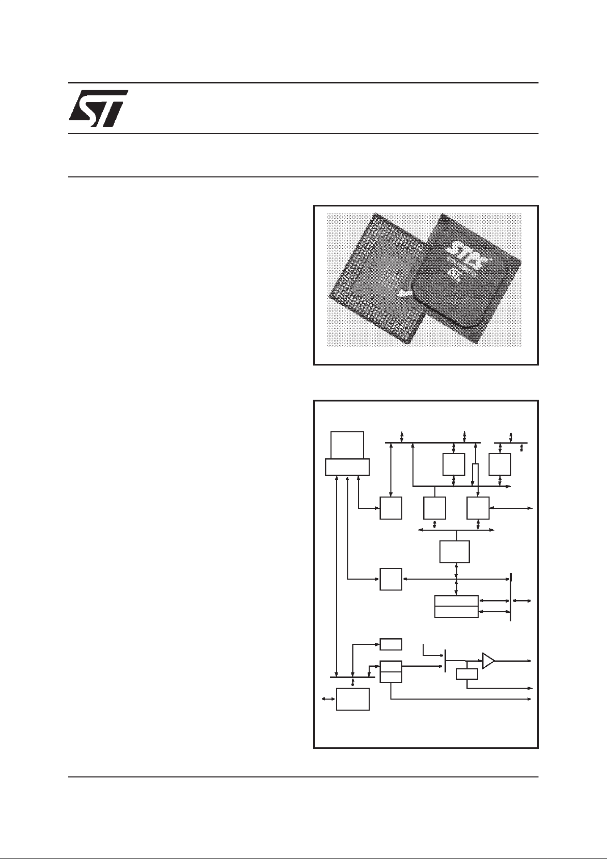
The device is packaged in a 388 Plastic Ball Grid
Array (PBGA).
TFT
ext
x86
Core
Host I/F
Serial2
// Port
Serial1
Kbd
Mouse
DRAM
I/F
VGA
GE
PCI
m/s
Local
Bus I/F
PCMCIA
CARDBUS
PCI BUS
IPC
82C206
PCI
CONTROLLER
ISA BUS
CRTC
HW Cursor
Monitor
TFT Output
SYNC Output
TFT I/F
PBGA388

STPC INDUSTRIAL
2/55
Issue 1.1
■ X86 Processor core
■ Fully static 32-bit 5-stage pipeline, x86
processor fully PC compatible.
■ Access up to 4GB of external memory.
■ 8Kbyte unified instruction and data cache
with write back capability.
■ Parallelprocessing integral floating point unit,
with automatic power down.
■ Clock core speeds up to 100 MHz.
■ Fully static design for dynamic clock control.
■ Low power and system management modes.
■ Optimized design for3.3V operation.
■ DRAM Controller
■ Integrated system memory and graphic frame
memory.
■ Supports up to 128-MByte system memory in
4 banks and down to as little as 2Mbytes.
■ Supports 4-MByte, 8-MByte, 16-MByte, and
32-MByte single-sided and double-sided
DRAM SIMMs.
■ Four quad-word write buffers for CPU to
DRAM and PCI to DRAM cycles.
■ Four quad-word read prefetch buffers for PCI
masters.
■ Supports Fast Page Mode & EDO DRAMs.
■ Programmable timing for DRAM parameters
including CAS pulse width, CAS pre-charge
time, and RAS to CAS delay.
■ 60, 70, 80 & 100ns DRAM speeds.
■ Memory hole between 1 MByte & 8 MByte
supported for PCI/ISA busses.
■ Hidden refresh.
■ Graphics Controller
■ 64-bit windows accelerator.
■ Complete backward compatibility to VGA and
SVGAstandards.
■ Hardware acceleration for text (generalized
bit map expansion), bitblts, transparent blts
and fills.
■ Up to 64 x 64 bit graphics hardware cursor.
■ Up to 4MB long linear frame buffer.
■ 8, 16, 24 and 32 bit pixels.
■ Drivers for Windows and other operating
systems.
■ CRT Controller
■ Integrated 135MHz triple RAMDAC allowing
for 1280 x 1024 x 75Hz display.
■ Requires external frequency synthesizer and
reference sources.
■ 8, 16,24 and 32-bit pixels.
■ Interlaced or non-interlaced output.
■ TFT Interface
■ Programmable panel size up to 1024 by 1024
pixels.
■ Support for 640 x 480, 800 x 600 & 1024 x
768 active matrix TFT flat panels with 9, 12,
18-bit interface.
■ Support 1 & 2 Pixels per Clock.
■ Programmable image positionning.
■ Programmable blank space insertion in text
mode.
■ Programmable horizontal and vertical image
expansion in graphic mode.
■ A fully programmable PWM (Pulse Width
Modulator) signals to adjust the flat panel
brightness and contrast.
■ Supports PanelLink
TM
high speed serial
transmitter externally for high resolution
panel interface.
■ PCI Controller
■ Fully compliant with PCI Version 2.1
specification.
■ Integrated PCI arbitration interface. Up to 3
masters can connect directly. External PAL
allows for greater than 3 masters.
■ Translation of PCI cycles to ISA bus.
■ Translation of ISA master initiated cycle to
PCI.
■ Support for burst read/write from PCImaster.
■ 0.33X and 0.5X CPU clock PCI clock.
■ Local Bus interface
■ 66MHz, low latency bus.
■ Asynchronous / synchronous.
■ 22-bit address and 16-bit data busses.
■ 2 Programmable Flash EPROM Chip Select.
■ 4 Programmable I/O Chip Select.
■ Separate memory and I/O address spaces.
■ Memory prefetch (improved performances).

STPC INDUSTRIAL
3/55
Issue 1.1
■ ISA master/slave
■ Generation of the ISA clock from either
14.318MHz oscillator clock or system clock
■ Programmable extra wait state for ISA cycles
■ Supports I/O recovery time for back to back
I/O cycles.
■ Fast Gate A20 and Fast reset.
■ Supports the single ROM that C, D, or E.
blocks shares with F blockBIOS ROM.
■ Supports flash ROM.
■ Supports ISA hidden refresh.
■ Buffered DMA & ISA master cycles to reduce
bandwidth utilization of the PCI and Host bus.
NSP compliant.
■ PC-Card interface
■ Support one PCMCIA 2.0 / JEIDA 4.1 68-pin
standard PC Card Socket.
■ Power Management support.
■ Support PCMCIA/ATA specifications.
■ Support I/O PC Card with pulse-mode
interrupts.
■ Provides an ExCA
TM
implementation to
PCMCIA 2.0 / JEIDA 4.1 standards.
■ DMA support.
■ Keyboard interface
■ Fully PC/AT&compatible
■ Mouse interface
■ Fully PS/2 compatible
■ Serial interface
■ 15540 compatible
■ Programmable word length, stop bits, parity.
■ 16-bit programmable baud rate generator.
■ Interrupt generator.
■ Loop-back mode.
■ 8-bit scratch register.
■ Two 16-bit FIFOs.
■ Two DMA handshake lines.
■ Parallel port
■ Standard Centronics mode supported.
■ Nibblemode supported.
■ Integrated Peripheral Controller
■ Two 8237/AT compatible 7-channel DMA
controllers.
■ Two 8259/AT compatible interrupt Controller.
16 interrupt inputs - ISA and PCI.
■ Three 8254 compatible Timer/Counters.
■ Co-processor error support logic.
■ Power Management
■ Four power saving modes: On, Doze,
Standby, Suspend.
■ Programmable system activity detector
■ Supports SMM.
■ Supports IO trap & restart.
■ Independent peripheral time-out timer to
monitor hard disk, serial & parallel ports.
■ Supports APM
■ Supports RTC,interrupt and DMA wake ups
ExCA is a trademark of PCMCIA / JEIDA.
PanelLink is a trademark of SiliconImage, Inc

GENERAL DESCRIPTION
4/55
Issue 1.1
1 GENERAL DESCRIPTION
At the heart of the STPC Industrial is an
advanced 64-bit processor block, dubbed the
5ST86. The 5ST86 includes a powerful x86
processor core along with a 64-bit DRAM
controller, advanced 64-bit accelerated graphics
and video controller, a high speed PCI local-bus
controller and Industry standard PC chip set
functions (Interrupt controller, DMA Controller,
Interval timer and ISA bus).
The STPC Industrial has in addition to the 5ST86
a TFT output, a Local Bus interface, PC Card and
super I/O features.
The STPC Industrial makes use of a tightly
coupled Unified Memory Architecture (UMA),
where the same memory array is used for CPU
main memory and graphics frame-buffer. This
means a reduction in total system memory for
system performances that are equal to that of a
comparable frame buffer and system memory
based system, and generally much better, due to
the higher memory bandwidth allowed by
attaching the graphics engine directly to the 64-bit
processor host interface running at the speed of
the processor bus rather than the traditional PCI
bus.
The 64-bit wide memory array provides the
system with 320MB/s peak bandwidth, double
that of an equivalent system using 32 bits. This
allows for higher resolution screens and greater
color depth. The processor bus runs at 66Mhz
further increasing “standard” bandwidth by at
least a factor of two.
The ‘standard’ PC chipset functions (DMA,
interrupt controller, timers, power management
logic) are integrated together with the x86
processor core; additional functions such as
communication ports are accessed by the STPC
Industrial via an internal ISA bus.
The PCI bus is the main data communication link
to the STPC Industrial chip. The STPC Industrial
translates appropriate host bus I/O and Memory
cycles onto the PCI bus. It also supports the
generation of Configuration cycles on the PCI
bus. The STPC Industrial, as a PCI bus agent
(host bridge class), fully complies with PCI
specification 2.1. The chip-set also implements
the PCI mandatory header registers in Type0 PCI
configuration space for easy porting of PCI aware
system BIOS. The device contains a PCI
arbitration function for three external PCI devices.
Graphics functions are controlled through the onchip SVGA controller and the monitor display is
produced through the 2D graphics display engine.
This Graphics Engine is tuned to work with the
host CPU to provide a balanced graphics system
with a low silicon area cost. It performs limited
graphics drawing operations which include
hardware acceleration of text, bitblts, transparent
blts and fills. The results of these operations
change the contents of the on-screen or offscreen frame buffer areas of DRAM memory. The
frame buffer can occupy a space up to 4 Mbytes
anywhere in the physical main memory.
The maximum graphics resolution supported is
1280x1024 in 65536 colours at 75Hz refresh rate
and is VGA and SVGA compatible. Horizontal
timing fields areVGA compatible while the vertical
fields are extended by one bit to accommodate
above display resolution.
To generate the TFT output, the STPC Industrial
extracts the digital video stream before the
RAMDAC and reformats it to the TFT format. The
height and width of the flat panel are
programmable through configuration registers up
to a size of 1024 by 1024.
By default, lower resolution images cover only a
part of the larger TFT panel. The STPC Industrial
allows to expand the image vertically and
horizontally in text mode by inserting
programmable blank pixels. It allows expantion of
the image vertically and horizontally in graphics
mode by replicating pixels. The replication of J
times every K pixel is independently
programmable in the vertical and horizontal
directions.
PanelLinkTMis a proprietary interconnect
protocol defined by Silicon Image, Inc. It consists
of a transmitter that takes parallel video/graphics
data from the host LCD graphics controller and
transmits it serially at high speed to the receiver
which controls the TFT panel. The TFT interface
is designed to support the connection of this
control signal to the PanelLinkTMtransmitter.
The STPC Industrial CARDBUS / PCMCIA
controller has been specifically designed to
provide the interface with PC-Cards which contain
additional memory or I/O and provides an
ExCATMimplementation to PCMCIA 2.0 / JEIDA
4.1 standards.
The power management control facilities include
socket power control, insertion/removal capability,
power saving with Windows inactivity, NCS
controlled Chip Power Down, together with further
controls for 3.3v suspend with Modem Ring
Resume Detection.

GENERAL DESCRIPTION
5/55
Issue 1.1
The need for system configuration jumpers is
eliminated by providing address mapping support
for PCMCIA 2.0 / JEIDA 4.1 PC-Card memory
together with address windowing support for I/O
space.
Selectable interrupt steering from PC-Card to
internal system bus is also provided.
The STPC Industrial implements a multi-function
parallel port. The standard PC/AT compatible
logical address assignments for LPT1, LPT2 and
LPT3 are supported.
The parallel port can be configured for any of the
following 3 modes and supports the IEEE
Standard 1284 parallel interface protocol
standards as follow:
-Compatibility Mode (Forward channel, standard)
-Nibble Mode (Reverse channel, PC compatible)
-Byte Mode (Reverse channel, PS/2 compatible)
The STPC Industrial BGA package has 388 balls,
but this is not sufficient for all the integrated
functions, therefore some features are sharing the
same balls and can not be used at the same time.
The STPC Industrial configuration is done by
‘strap options’. It is a set of pull-up or pull-down
resistors on the memory data bus, checked on
reset, which auto-configure the STPC Industrial.
We can distinguish three main blocks
independently configurables
: The ISA / Local
Bus block, the Serial 1 / TFT block, and the PCI /
PC Card block.
From the first block,we can activateeither the ISA
bus and some IPC additionnal features, or the
Local bus, the parallel port and the second serial
interface.
From the second block, we can activate either the
first serial port, or the TFT extension to get from 4
bit per colour to 6 bit per colour.
From the third block, we can activate either the
PCI bus, or the PC Card interface (CardBus/
PCMCIA/ZoomVideo).
The STPC Industrial core is compliant with the
Advanced Power Management (APM)
specification to provide a standard method by
which the BIOS can control the power used by
personal computers. The Power Management
Unit module (PMU) controls the power
consumption providing a comprehensive set of
features that control the power usage and
supports compliance with the United States
Environmental Protection Agency’s Energy Star
Computer Program. The PMU provides following
hardware structures to assist the software in
managing the power consumption by the system.
- System Activity Detection.
- 3 power-down timers detecting system inactivity:
- Doze timer (short durations).
- Stand-by timer (medium durations).
- Suspend timer (long durations).
- House-keeping activity detection.
- House-keeping timer to cope with short bursts of
house-keepingactivity while dozing or in stand-by
state.
- Peripheral activity detection.
- Peripheral timer detecting peripheral inactivity
- SUSP# modulation to adjust the system
performance in various power down states of the
system including full power on state.
- Power control outputs to disable power from
different planes of the board.
Lack of system activity for progressively longer
periods of time is detected by the three power
down timers. These timers can generate SMI
interrupts to CPU so that the SMM software can
put the system in decreasing states of power
consumption. Alternatively, system activity in a
power down state can generate SMI interrupt to
allow the software to bring the system back up to
full power on state. The chip-set supports up to
three power down states described above, these
correspond to decreasing levels ofpower savings.
Power down puts the STPC Industrial into
suspend mode. The processor completes
execution of the current instruction, any pending
decoded instructions and associated bus cycles.
During the suspend mode, internal clocks are
stopped. Removing power down, the processor
resumes instruction fetchingand begins execution
in the instruction stream at the point it had
stopped. Because of the static nature of the core,
no internal data is lost..

GENERAL DESCRIPTION
6/55
Issue 1.1
Figure 1.1. Functionnal description.
x86
Core
Host I/F
Serial 2
// Port
Serial 1
DRAM
I/F
VGA
GE
PCI m/s
Local
Bus I/F
PCMCIA
CARDBUS
PCI BUS
ISA
m/s
IPC
82C206
PCI m/s
ISA BUS
CRTC
HW Cursor
Monitor
TFT Output
SYNC Output
TFT I/F
TFT
extension
Kbd
Mouse

GENERAL DESCRIPTION
7/55
Issue 1.1
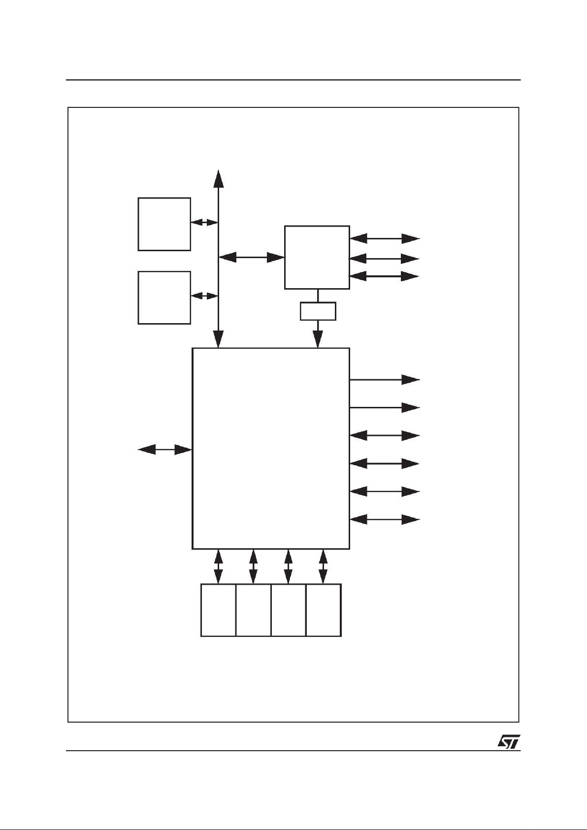
Figure 1.2. PCI, PCMCIA & CARDBUS modes:
PCI m/s
PCMCIA
CARDBUS
PCI BUS
PCI m/s
PCMCIA
CARDBUS
PCI BUS
PCI m/s
PCMCIA
CARDBUS
PCI BUS

GENERAL DESCRIPTION
8/55
Issue 1.1
Figure 1.3. Local Bus and ISA bus modes:
Figure 1.4. TFT in normal (serial 1 available) and extended modes (serial 1 unavailable).
Serial 2
// Port
Local
Bus I/F
ISA
m/s
IPC
82C206
ISA BUS
Serial 2
// Port
Local
Bus I/F
ISA
m/s
IPC
82C206
ISA BUS
Serial 1 TFT
extension
TFT
extension
TFT Output
TFT I/F
Kbd
Mouse
Serial 1Kbd
Mouse
TFT Output
TFT I/F
9-bit mode
12-bit mode
18-bit mode
2 x 9-bit mode
GENERAL DESCRIPTION
9/55
Issue 1.1
Figure 2. Typical PC oriented Application
ISA
PCI
4x 16-bit EDO DRAMs
Super I/O
Flash
IDE
Serial Ports
Parallel Port
Floppy
Monitor
TFT
SVGA
IRQ
DMA.REQ
DMA.ACK
DMUX
MUX
MUX
STPC Industrial
RTC
Mouse
Keyboard
GENERAL DESCRIPTION
10/55
Issue 1.1
Figure 3. Typical Embedded Application
STPC Industrial
PC-Card
4x 16-bit EDO DRAMs
Flash
Peripheral
IRQ
MUX
PCMCIA
CARDBUS
Monitor
TFT
SVGA
Mouse
Keyboard
Serial Ports
Parallel Port
STPC Local Bus
I/O
SRAM
STRAP OPTION
11/55
Issue 1.1
2 STRAP OPTION
This chapter defines the STPC Industrial Strap Options and their location
Memory
Data
Lines
Refer to Designation Location
Actual
Settings
Set to ’0’ Set to ’1’
MD0 - Reserved - - - MD1 - Reserved - - - MD2 DRAM Bank 1 Speed Index 4A,bit 2 User defined 70 ns 60 ns
MD3 Speed Index 4A,bit 3 Pull up
MD4 Type Index 4A,bit 4 User defined EDO FPM
MD5 DRAM Bank 0 Speed Index 4A,bit 5 User defined 70 ns 60 ns
MD6 Speed Index 4A,bit 6 Pull up
MD7 Type Index 4A,bit 7 User defined EDO FPM
MD8 - Reserved - - - -
MD9 - Reserved - - - MD10 DRAM Bank 3 Speed Index 4B,bit 2 User defined 70 ns 60 ns
MD11 Speed Index 4B,bit 3 Pull up
MD12 Type Index 4B,bit 4 User defined EDO FPM
MD13 DRAM Bank 2 Speed Index 4B,bit 5 User defined 70 ns 60 ns
MD14 Speed Index 4B,bit 6 Pull up
MD15 Type Index 4B,bit 7 User defined EDO FPM
MD16 Reserved Index 4C,bit 0
MD17 PCI Clock PCI_CLKO Divisor Index 4C,bit 1 User defined HCLK / 3 HCLK / 2
MD18 Host Clock HCLK Pad Direction Index 4C,bit 2 User defined External Internal
MD19 Graphics Clock GCLK2x Pad Direction Index 4C,bit 3 User defined External Internal
MD20 DOT Clock DCLK Pad Direction Index 4C,bit 4 User defined External Internal
MD21 Reserved Pull up
MD22 External IPC Debug Option Index 5F,bit 1 Pull up External IPC Internal IPC
MD23 - Reserved Index 5F,bit 2 Pull up - MD24 HCLK HCLK PLL Speed Index 5F,bit 3 User defined 000 25 MHz
MD25 Index 5F,bit 4 User defined 001 33 MHz
MD26 Index 5F,bit 5 User defined 010 40 MHz
011 50 MHz
100 60 MHz
101 66 MHz
110 75 MHz
111 80 MHz
MD27 Reserved Pull down
MD28 Reserved Pull down
MD29 Reserved Pull down
MD30 Reserved Pull down
MD31 Reserved Pull down
MD32 Reserved Pull down
MD33 Reserved Pull up
MD34 Reserved Pull down
MD35 Reserved Pull up
MD 36 Reserved Pull up
MD 37 Reserved Pull up
MD 38 Reserved Pull up
STRAP OPTION
12/55
Issue 1.1
2.1 STRAP OPTION REGISTER DESCRIPTION
2.1.1 STRAP REGISTER 0 INDEX 4AH (STRAP0)
Bits 7-0, This register reflect the status of pins MD[7:0] respectively. They are expected to be connected
on the system board to the SIMM configuration pins as follows:
Note that the SIMM speed and type information read here is meant only for the software and is not used
by thehardware. The software must program the Host and graphics DRAM controller configuration registers appropriately based on these bits.
This register defaults to the values sampled on MD[7:0] pins after reset.
MD 39 Reserved Pull up
MD 40 PCMCIA or PCI i/f 3C,bit 0 User defined PCI PCMCIA
MD 41 Local Bus or ISA i/f 3C,bit 1 User defined ISA Local Bus
MD 42 Key Board & Mouse 3C,bit 2 User defined External Internal
MD 43 Parallel Port 3C,bit 3 User defined External Internal
MD 44 Serial Port UART1 3C,bit 4 User defined External Internal
MD 45 UART2 3C,bit 5 User defined External Internal
MD 46 Reserved 3C,bit 6 Pull down
MD 47 Reserved 3C,bit 7 Pull down
MD 48 TFT Outputs on RFU pads 3D,bit 0 User defined Disable Enable
MD 49 Cardbus Socket 5V Availability 3D,bit 1 User defined
Not Availa-
ble
Available
MD 50 3.3V Availability 3D,bit 2 User defined
Not Availa-
ble
Available
MD 51 x.xV Available 3D,bit 3 User defined
Not Availa-
ble
Available
MD 52 y.yV Available 3D,bit 4 User defined
Not Availa-
ble
Available
MD 53 Reserved Pull uo
MD 56 Reserved Pull up
MD 57 Reserved Pull down
MD 58 Reserved Pull up
MD 59 Reserved Pull down
Bit Sampled Description
Bit 7 SIMM 0 DRAM type
Bits 6-5 SIMM 0 speed
Bit 4 SIMM 1 DRAM type
Bits 3-2 SIMM 1 speed
Bits 1-0 Reserved
Memory
Data
Lines
Refer to Designation Location
Actual
Settings
Set to ’0’ Set to ’1’

STRAP OPTION
13/55
Issue 1.1
2.1.2 STRAP REGISTER 1 INDEX 4BH (STRAP1)
Bits 7-0, This register reflect the status of pins MD[15:8] respectively. They are expected tobe connected
on the system board to the SIMM configuration pins as follows:
Note that the SIMM speed and type information read here is meant only for the software and is not used
by the hardware. The software must program the Host and graphics dram controller configuration registers appropriately based on these bits.
This register defaults to the values sampled on MD[15:8] pins after reset.
2.1.3 STRAP REGISTER 2 INDEX 4CH (STRAP2)
Bits 4-0of this register reflect the status of pins MD[20:16] respectively. Bit 5 ofthis register reflect the status of pin MD[23]. Bit 4 is writeable, writes to other bits in this register have no effect.
They are use by the chip as follows:
Bits 7-5, Reserved
Bit 4, This bit reflects the value sampled on MD[20] pin and controls the Dot clock (DCLK) source. Note
this bit is writeable as well as readable.
Bit 3, This bit reflects the value sampled on MD[19] pin and controls the Graphics clock source.
Bit 2, This bit reflects the value sampled on MD[18] pin and controls the Host/CPU clock source as follows: setting to’0’: External. HCLK pin is an input, setting to ’1’: Internal. HCLK pin is an output and is connected to the internal frequency synthesizer output.
Bit 1, This bit reflects the value sampled on MD[17] pin and controls the PCI clock output as follows:
Setting to ’0’, the PCI clock output = HCLK / 3
Setting to ’1’, the PCI clock output = HCLK / 2
Bit 0, Reserved.
This register defaults to the values sampled on MD[23] & MD[20:16] pins after reset.
Bit Sampled Description
Bit 7 SIMM 2 DRAM type
Bits 6-5 SIMM 2 speed
Bit 4 SIMM 3 DRAM type:
Bits 3-2 SIMM 3 speed
Bit 1-0 Reserved

STRAP OPTION
14/55
Issue 1.1
2.1.4 STRAP REGISTER 3 INDEX 3CH (STRAP3)
Bits 7-0 of this register reflect the status of pins MD[47:40] respectively.
They are use by the chip as follows:
Bit 7-6, Reserved.
Bit 5, UART2 internal or external. This bit reflects the value sampled on MD[45] pin and controls the
UART2 I/F as follows:
Setting to ’0’, UART2 is external.
Setting to ’1’, UART2 is internal.
Bit 4, UART1 internal or external and additional TFT outputs. This bit reflects the value sampled on
MD[44] pin and controls the UART1 I/F and the additional TFT I/F as follows:
Setting to ’0’, UART1 is external and anadditional 6 TFT outputs (lowest bits - 2 red, 2 green
and 2 blue) are enabled.
Setting to ’1’, UART1 is internal.
Note that when strap option testbus enabled (see Section 2.1.3 Strap Register 2 bit 0) is driven to 1 it
takes priority over this strap which becomes meaningless.
Bit 3, Parallel Port internal or external. This bitreflects the value sampled on MD[43] pin and controls the
Parallel Port i/f as follows:
Setting to ’0’, the Parallel Port is external
Setting to ’1’, the Parallel Port is internal
Bit 2, KB/Mouse internal or external. This bit reflects the value sampled on MD[42] pin and controls the
KB/Mouse controller i/f as follows:
Setting to ’0’, the KB/Mouse controller is external
Setting to ’1’, the KB/Mouse controller is internal
Bit 1, Local Bus i/for ISA I/F. This bit reflects thevalue sampled on MD[41] pin and sets whether the Local Bus i/f or the ISA i/f is available at the device i/f as follows:
Setting to ’0’, selectes the ISA I/F
Setting to ’1’, selectec the Local Bus I/F
Bit 0 PCMCIA I/F or PCI I/F. This bit reflects the value sampled on MD[40] pin and sets whether the
PCMCIA i/f or the PCI i/f is available at the device i/f as follows:
Setting to ’0’, selects the PCI I/F
Setting to ’1’, selects the PCMCIA I/F
This register defaults to the values sampled on MD[47:40] pins after reset.

STRAP OPTION
15/55
Issue 1.1
2.1.5 STRAP REGISTER 4 INDEX 3Dh (STRAP4)
Bits 5-0 of this register reflect the status of pins MD[53:48] respectively.
They are use by the chip as follows:
Bits 7-5 Reserved.
Bit 4, y.y V present on board. This bit reflects the value sampled on MD[52] pin and is used to notify the
Cardbus socket management unit if the y.y V vcc voltage (where y.y is less than x.x) is present on board
as follows
Setting to ’0’, y.y V Vcc voltage is not available
Setting to ’1’: y.y V Vcc voltage is available.
Bit 3, x.x V present on board. This bit reflects the value sampled on MD[51] pin and is used to notify the
Cardbus socket management unit if the x.x V vcc voltage (where x.x is less than 3.3) is present on board
as follows:
Setting to ’0’, x.x V Vcc voltage is not available.
Setting to ’1’: x.x V Vcc voltage is available.
Bit 2, 3.3 V present on board. This bit reflects the value sampled on MD[50] pin and is usedto notify the
Cardbus socket management unit if the 3.3 V vcc voltage is present on board as follows:
Setting to ’0’, 3.3 V vcc voltage is not available.
Setting to ’1’, 3.3 V vcc voltage is available.
Bit 1, 5 V present on board. This bit reflects the value sampled on MD[49] pin and is used to notify the
Cardbus socket management unit if the 5 V vcc voltage is present on board as follows:
Setting to ’0’, 5 V vcc voltage is not available.
Setting to ’1’, 5 V vcc voltage is available.
Bit 0, This bit reflects the value sampled on MD[48] pin and is used to enable the TFT controller outputs
on pads RFU0-RFU11 as follows:
RFU0 : R[2]
RFU1 : R[3]
RFU2 : R[4]
RFU3 : R[5]
RFU4 : G[2]
RFU5 : G[3]
RFU6 : G[4]
RFU7 : G[5]
RFU8 : B[2]
RFU9 : B[3]
RFU10 : B[4]
RFU11 : B[5]
This register defaults to the values sampled on MD[53:48] pins after reset.

STRAP OPTION
16/55
Issue 1.1
2.1.6 HCLK PLL STRAP REGISTER 0 INDEX 5FH (HCLK_STRAP0)
Bits 5-0 of this register reflect the status of pins MD[26:21] respectively.
They are use by the chip as follows:
Bits 7-6, Reserved.
Bits 5-3,These pins reflect the value sampled on MD[26:24] pinsrespectively and control the Host clock
frequency synthesizer.
Bit 2-1, Reserved.
Bit 0, Reserved.
This register defaults to the values sampled on above pins after reset.

PIN DESCRIPTION
17/55
Issue 1.1
3 PIN DESCRIPTION
3.1. INTRODUCTION
The STPC Industrial integrates most of the functionalities of the PC architecture. Therefore, many
of the traditional interconnections between the
host PC microprocessor and the peripheral devices are totally internal to the STPC Industrial. This
offers improved performance due to the tight coupling of theprocessor coreand it’s peripherals. As
a result many of the external pin connections are
made directly to the on-chip peripheral functions.
Figure 3-1 shows the STPC Industrial’s external
interfaces. It defines the main busses and their
function. Table 3-1 describes the physical implementation listing signal types and their functionalities. Table 3-2 provides a full pin listing and description.
Table 3-4 provides a full listing of theSTPC Industrial package pin location physical connection.
Please refer tothe pin allocation drawing for reference.
Due to the number of pins available for the package, and the number offunctional I/Os, some pins
have several functions, selectable by strap option
on Reset. Table 3-3 provides a summary of these
pins and their functions.
Table 3-1. Signal Description
Group name Qty
Basic Clocks, Reset & Xtal (SYS) 13
DRAM Controller(DRAM) 89
PCI Controller 55
64
PC Card Interface 64
Keyboard/Mouse Controller (SIO) 4
Local Bus I/F, Parallel I/F,Serial 2 75
75
ISA Interface/IPC extensions 73
Serial 1 (SIO) 8
26
TFT output 24
VGA Controller (VGA) 10
Grounds 74
V
DD
16
Analog specific V
CC/VDD
16
Reserved 1
TotalPin Count 388
Figure 3-1. STPC Industrial External Interfaces
PCI
x86 core
DRAM VGA TFT SYS SIO
89 10 24 12 55
13
75 38
STPC Industrial
CARD
PC
ISA/
LOCAL BUS
NORTH BRIDGE SOUTH BRIDGE

PIN DESCRIPTION
18/55
Issue 1.1
Table 3-2. Definition of Signal Pins
Signal Name Dir Description Qty
BASIC CLOCKS AND RESETS
SYSRSTI#* I System Reset / Power good 1
SYSRSTO#* O Reset Output to System 1
XTALI I 14.3MHz Crystal Input 1
XTALO O 14.3MHz Crystal Output 1
PCI_CLKI* I 33MHz PCI/CardBus Input Clock 1
PCI_CLKO O 33MHz PCI/CardBus Output Clock 1
ISA_CLK, ISA_CLK2X O ISA Clock x1 and x2 (also Multiplexer Select Line For IPC) 2
CLK14M O ISA bus synchronisation clock 1
HCLK* I/O 33 / 66MHz Host Clock (Test) 1
DEV_CLK* O 24MHz Peripheral Clock 1
GCLK2X I/O 80MHz Graphics Clock 1
DCLK I/O 135MHz Dot Clock 1
V
DD
_xxx_PLL Power Supply for PLL Clocks
MEMORY INTERFACE
MA[11:0] I/O Memory Address 12
RAS#[3:0] O Row Address Strobe 4
CAS#[7:0] O Column Address Strobe 8
MWE# O Write Enable 1
MD[63:0] I/O Memory Data 64
LOCAL BUS INTERFACE(COMBINED WITH ISA BUS )
PA[21:0]* O Address Bus [21:0] 22
PD[15:0]* I/O Data Bus [15:0] 16
PRDY#* I Ready 1
PWR#[1:0]* O Memory and I/O Write signals 2
PRD#[1:0]* O Memory and I/O Read signals 2
FCS#[1:0]*, IOCS#[3:0]* O Flash Memory and I/O Chip Select 6
ISA BUS INTERFACE (COMBINED WITH LOCAL BUS, PARALLEL PORT, SERIAL INTERFACE)
LA[23:17]* O Unlatched Address 7
SA[19:0]* O Latched Address 20
SD[15:0]* I/O Data Bus 16
IOCHRDY* I I/O Channel Ready 1
ALE* O Address Latch Enable 1
BHE#* O System Bus High Enable 1
MEMR#*, MEMW#* I/O Memory Read & Write 2
SMEMR#*, SMEMW#* O System Memory Read and Write 2
IOR#*, IOW#* I/O I/O Read and Write 2
MASTER#* I Add On Card Owns Bus 1
MCS16#*, IOCS16#* I Memory Chip Select 16, I/O Chip Select 16 2
REF#* I Refresh Cycle 1
AEN* O Address Enable 1
IOCHCK#* I I/O Channel Check (ISA) 1
RTCRW#* O RTC Read / Write# 1
RTCDS#* O RTC Data Strobe 1
RTCAS#* O RTC Address Strobe 1

PIN DESCRIPTION
19/55
Issue 1.1
RMRTCCS#* O ROM / RTC Chip Select 1
GPIOCS#* I/O General Purpose Chip Select 1
IRQ_MUX[3:0]* I Multiplexed Interrupt Request 4
DACK_ENC[2:0]* O DMA Acknowledge 3
DREQ_MUX[1:0]* I Multiplexed DMA Request 2
TC* O ISA Terminal Count 1
KEYBOARD & MOUSE INTERFACE
KBDATA*,MDATA* I Keyboard & Mouse Data Line 2
KBCLK*, MCLK* O Keyboard & Mouse Clock Line 2
SERIAL INTERFACE (SERIAL 1 COMBINED WITH TFT INTERFACE / SERIAL 2 COMBINED WITH IPC )
SIN1*, SIN2* I Serial Data In (Serial 1, 2) 2
SOUT1*, SOUT2* O Serial Data Out (Serial 1, 2) 2
CTS1#*, CTS2#* I Clear ToSend (Serial 1, 2) 2
RTS1#*, RTS2#* O Request ToSend (Serial 1, 2) 2
DSR1#*, DSR2#* I Data Set Ready (Serial 1, 2) 2
DTR1#*, DTR2#* O Data Terminal Ready (Serial 1,2) 2
DCD1#*, DCD2#* I Data Carrier Detect (Serial 1, 2) 2
RI1#*, RI2#* I Ring Indicator (Serial 1, 2) 2
PARALLEL PORT (COMBINED WITH ISA BUS AND IPC)
PE* I Paper End 1
SLCT* I SELECT 1
BUSY#* I BUSY 1
ERR#* I ERROR 1
ACK#* I Acknowledge 1
PDDIR#* O Parallel Device Direction 1
STROBE#* O PCS / STROBE# 1
INIT#* O INIT 1
AUTPFDX#* O Automatic Line Feed 1
SLCTIN#* O SELECT IN 1
PPD[7:0]* I/O Data Bus 8
PCMCIA INTERFACE(COMBINED WITH PCI / CARDBUS)
RESET* O Reset 1
A[25:0]* O Address Bus 26
D[15:0]* I/O Data Bus 16
IORD#*, IOWR#* O I/O Read and Write 2
DREQ#* / WP*/ IOIS16#* I DMA Request // Write Protect // I/O Size is 16 bit 1
BVD1*, BVD2* I Battery Voltage Detect 2
READY#*/BUSY#*/IREQ#* I Ready / Busy // Interrupt Request 1
WAIT#* I Wait 1
INPACK#* I Input Port Acknowledge 1
OE#* / TCw* O Output Enable // DMA Terminal Count 1
WE#* / TCr* O Write Enable // DMA Terminal Count 1
DACK* / REG#* O DMA Acknowledge // Register 1
CD1#*, CD2#* I Card Detect 2
Table 3-2. Definition of Signal Pins
Signal Name Dir Description Qty

PIN DESCRIPTION
20/55
Issue 1.1
CE1#*, CE2#* O Card Enable 2
VS1#*, VS2#* I VoltageSense 2
VCC5_EN* O Power Switch control : 5v power 1
VCC3_EN* O Power Switch control : 3.3v power 1
VPP_PGM* O Power Switch control : Program power 1
VPP_VCC* O Power Switch control : VCC power 1
CARDBUS INTERFACE(COMBINED WITH PCI / PCMCIA)
CCLKRUN* I/O Clock 1
CRST#* O Reset 1
CSTSCHG#* I System Change 1
CAD[31:0]* I/O Address / Data 32
CBE[3:0]* I/O Bus Commands / Byte Enables 4
CFRAME#* I/O Cycle Frame 1
CTRDY#* I/O Target Ready 1
CIRDY#* I/O Initiator Ready 1
CSTOP#* I/O Stop Transaction 1
CDEVSEL#* I/O Device Select 1
CPAR* I/O Parity Signal Transactions 1
CSERR#* I System Error 1
CPERR#* I/O Parity Error 1
CBLOCK#* I/O PCI Lock 1
CCD[2:1]* I Card Detect 2
CINT#* I Interrupt Request 1
CREQ#* I Request 1
CGNT#* O Grant 1
PCI INTERFACE(COMBINED WITH PCMCIA / CARDBUS)
AD[31:0]* I/O Address / Data 32
BE[3:0]* I/O Bus Commands / Byte Enables 4
FRAME#* I/O Cycle Frame 1
TRDY#* I/O Target Ready 1
IRDY#* I/O Initiator Ready 1
STOP#* I/O Stop Transaction 1
DEVSEL#* I/O Device Select 1
PAR* I/O Parity Signal Transactions 1
SERR#* O System Error 1
LOCK#* I PCI Lock 1
PCI_REQ#[2:0]* I PCI Request 3
PCI_GNT#[2:0]* O PCI Grant 3
PCI_INT[3:0]* I PCI Interrupt Request 4
Table 3-2. Definition of Signal Pins
Signal Name Dir Description Qty

PIN DESCRIPTION
21/55
Issue 1.1
Note; *denotes theat the pin is V5T(see Section 4
)
MONITOR INTERFACE
RED, GREEN, BLUE O Red, Green, Blue 3
VSYNC* I/O Vertical Sync 1
HSYNC* I/O Horizontal Sync 1
VREF_DAC I DAC Voltage reference 1
RSET I Resistor Set 1
COMP I Compensation 1
DDC[1:0]* I/O Display Data Channel Serial Link 2
SCL / DDC[1]* I/O I C Interface - Clock / Can be used fo r VG A DDC[1] signal 1
SDA / D DC[0]* I/O I C Interface - Data / Can be used fo r VG A DDC[0] signal 1
TFT INTE RFACE(COMBINE D W ITH S ERIAL 1)
R[5:0], G[5:0], B[ 5:0] O Red, G reen, Blue 18
FPLINE O H orizontal S ync 1
FPFRAME O Vertical S ync 1
DE O Data Enable 1
ENAVDD O E nable Vd d of f lat panel 1
ENVCC O E nable Vc c of fl at panel 1
PWM O P WM back-light control 1
MISCELLA NEO US
SPKRD* O S peaker Device Outp ut 1
SCAN_ENABLE I Test Pin - Reserved 1
Table 3-2. Definition of Signal Pi ns
Signal Name Dir Description Qty

PIN DESCRIPTION
22/55
Issue 1.1
3.2. SIGNAL DESCRIPTIONS
3.2.2 BASIC CLOCKS AND RESETS
SYSRSTI#
System Reset/Power good.
This input
is low when the reset switch is depressed. Otherwise, it reflects the power supply’s power good
signal. PWGD is asynchronous to all clocks, and
acts as a negative active reset. The reset circuit
initiates a hard reset on the rising edge of PWGD.
SYSRSTO#
Reset Output to System.
This is the
system resetsignal and is used to reset the rest of
the components (not on Host bus) in the system.
The ISA bus reset is an externally inverted buffered versionof this output and the PCIbus resetis
an externally buffered version of this output.
XTALI
14.3MHz Crystal Input
XTALO
14.3MHz Crystal Output.
These pins are
the 14.318MHz crystalinput; This clock isused as
the reference clock for the internal frequency synthesizer to generate the HCLK and CLK24M.
A 14.318 MHz Series Cut Quartz Crystal should
be connected between these two pins. Balance
capacitors of 15 pF should also be added. In the
event of an external oscillatorproviding the master
clock signalto the STPC Industrialdevice, the TTL
signal should be provided on XTALO.
PCI_CLKI
33MHz PCI Input Clock
This signal must be connected to a clock generator and is usually connected to PCI_CLKO.
PCI_CLKO
33MHz PCI Output Clock.
This is the
master PCI bus clock output
ISA_CLK
ISA Clock Output (also Multiplexer Se-
lect Line For IPC).
This pin produces the Clock
signal for the ISA bus. It is also used with
ISA_CLK2X as the multiplexor control lines for the
Interrupt Controller Interrupt input lines. This is a
divided down version of the PCICLK or OSC14M.
ISA_CLKX2
ISA Clock Output (also Multiplexer
Select Line For IPC).
This pin produces a signal at
twice the frequency of the ISA bus Clock signal. It
is also used with ISA_CLK as the multiplexor control lines for the Interrupt Controller Interrupt input
lines.
CLK14M
ISA bus synchronisation clock.
This is
the buffered 14.318 Mhzclock to the ISA bus. This
clock also provides the reference clock to the frequency synthesizer that generates GCLK2X and
DCLK.
HCLK
Host Clock.
This is the host 1X clock. Its
frequency can vary from 50 to 75 MHz. All host
transactions and PCI transactions are synchronized to this clock. Host transactions executed by
the DRAM controller are also driven by this clock.
DEV_CLK
24MHz Peripheral Clock (floppydrive).
This 24MHZ signal is provided as a convenience
for the system integration of a Floppy Disk driver
function in an external chip.
GCLK2X
80MHz Graphics Clock.
This is the
Graphics 2X clock, which drives the graphics engine and the DRAM controller to execute the
graphics and display cycles.
Normally GCLK2X isgenerated by the internal frequency synthesizer, and this pin is an output. By
setting a bit in Strap Register 2, this pin can be
made an input so that an external clock can replace the internal frequency synthesizer.
DCLK
135MHz Dot Clock.
This is the dot clock,
which drivesgraphics display cycles.Its frequency
can be as high as 135 MHz, and it is required to
have a worst case duty cycle of 60-40. For further
details, refer to Section 2.1.3 bit 4.
3.2.3 MEMORY INTERFACE
MA[11:0]
Memory Address.
These 12 multiplexed
memory addresspins support external DRAM with
up to 4K refresh. These include all 16M x N and
some 4M x N DRAM modules. The address signals must be externally buffered to support more
than 16 DRAM chips. The timing of these signals
can be adjusted by software to match the timings
of most DRAM modules.
MD[63:0]
Memory Data.
This is the 64-bit memory
data bus. If only half of a bank is populated,
MD63-32 is pulled high, data is on MD31-0.
MD20-0 are also used as inputs at the rising edge
of PWGD to latch in power-up configuration information into the ADPC strap registers.

PIN DESCRIPTION
23/55
Issue 1.1
RAS#[3:0]
Row Address Strobe.
There are 4 active low row address strobe outputs, one each for
each bank of the memory. Each bank contains 4
or 8-Bytes of data. The memory controller allows
half of a bank (4-Bytes) to be populated to enable
memory upgrade at finer granularity.
The RAS# signals drive the SIMMs directly without any external buffering. These pins are always
outputs, but they can also simultaneously be inputs, toallow the memory controller to monitor the
value of the RAS# signals at the pins.
CAS#[7:0]
Column Address Strobe.
There are 8
active low column address strobe outputs, one
each for each Byte of the memory.
The CAS# signals drive the SIMMs either directly
or through external buffers.
These pins are always outputs, but they can also
simultaneously be inputs, to allow the memory
controller to monitor the value of the CAS# signals
at the pins.
MWE#
Write Enable.
Write enable specifies
whether the memory access is a read (MWE# = H)
or a write (MWE# = L). This single write enable
controls all DRAMs. It can be externally buffered
to boost the maximum number of loads (DRAM
chips) supported.
The MWE# signals drive the SIMMs directly without any external buffering.
3.2.4 LOCAL BUS INTERFACE
(Combined with ISA Bus)
PA[21:0]
Memory Address.
This is the 22-bit Lo-
cal Bus Address
PD[15:0]
Data Bus.
This is the 16-bit bidirectional
Local Bus Data bus.
PRDY#
Ready.
This input signals the Local Bus
Ready state.
PWR#1
Memory and I/O Write signal
for MS Byte
PWR#0
Memory and I/O Write signal
for LS Byte
.
PRD#1
Memory and I/O Read signals
for MS
Byte
.
PRD#0
Memory andI/O Read signals
for LS Byte
.
FCS#[1:0], IOCS#[3:0]
Flash Memory and I/O
Chip select.
3.2.5 ISA BUS INTERFACE
LA[23:17]
Unlatched Address.
These unlatched
ISA Bus pins address bits 23-17 on 16-bit devices.
When the ISA bus is accessed by any cycle initiated from the PCI bus, these pins are in output
mode. When an ISA bus master owns the bus,
these pins are tristated.
SA[19:0]
Unlatched Address.
These are the 20
low bits of the system address bus of ISA. These
pins are used as an input when an ISA busmaster
owns the bus and are outputs at all other times.
SD[15:0]
I/O Data Bus (ISA).
These are the exter-
nal ISA databus pins.
IOCHRDY
IOChannel Ready.
IOCHRDY is the IO
channel ready signal of the ISA bus and is driven
as an output in response to an ISA master cycle
targeted to the host bus or an internal register of
the STPC Industrial. The STPC Industrial monitors this signal as an input when performing an
ISA cycle on behalf of the host CPU, DMA master
or refresh.
ISA masters which do not monitor IOCHRDY are
not guaranteed to work with the STPC Industrial
since the access to the system memory can be
considerably delayed due to CRT refresh or a
write back cycle.
ALE
Address Latch Enable.
This is the address
latch enable output of the ISA bus and is asserted
by the STPC Industrial to indicate that LA23-17,
SA19-0, AEN and SBHE# signals are valid. The
ALE is driven high during refresh, DMA master or
an ISA master cycles by the STPC Industrial.
ALE is driven low after reset.
BHE#
System Bus HighEnable.
This signal,when
asserted, indicates that a data Byte is being transferred on SD15-8 lines. It is used as an input when
an ISA master owns the bus and is an output at all
other times.
MEMR#
Memory Read.
This is the memory read
command signal of the ISAbus. It is used as an input when an ISA master owns the bus and is an
output at all other times.
The MEMR# signal is active during refresh.
MEMW#
Memory Write.
This is the memory write
command signal of the ISAbus. It is used as an input when an ISA master owns the bus and is an
output at all other times.

PIN DESCRIPTION
24/55
Issue 1.1
SMEMR#
System Memory Read.
The STPC Industrial generates SMEMR# signal of the ISA bus
only when the address is below one MByte or the
cycle is a refresh cycle.
SMEMW#
System Memory Write.
The STPC Industrial generatesSMEMW# signal of the ISA bus
only when the address is below one MByte.
IOR#
I/O Read.
This is the IO read command signal of the ISA bus. It is an input when an ISA master owns the bus and is an output at all other
times.
IOW#
I/O Write.
This is the IO write command signal of the ISA bus. It is an input when an ISA master owns the bus and is an output at all other
times.
MASTER#
Add On CardOwns Bus.
This signal is
active when an ISA device has been granted bus
ownership.
MCS16#
Memory Chip Select16.
This is the decode of LA23-17 address pins of the ISA address
bus without any qualification of the command signal lines. MCS16# is always an input. The STPC
Industrial ignores this signal during IO and refresh
cycles.
IOCS16#
IO Chip Select16.
This signal is the decode of SA15-0 address pins of the ISA address
bus without any qualification of the command signals. The STPC Industrial does not driveIOCS16#
(similar to PC-AT design). An ISA master access
to an internal register of the STPC Industrial is executed as an extended 8-bit IO cycle.
REF#
Refresh Cycle.
This is the refresh command
signal of the ISA bus. It is driven as an output
when the STPC Industrial performs arefresh cycle
on the ISA bus. It is used as an input when an ISA
master owns the bus and is used to trigger a refresh cycle.
The STPC Industrial performs a pseudo hidden
refresh. It requests the host bus for two host
clocks to drive the refresh address and capture it
in external buffers. The host bus is then relinquished while the refresh cycle continues on the
ISA bus.
AEN
Address Enable.
Address Enable is enabled
when the DMA controller is the bus owner to indicate that a DMA transfer will occur. The enabling
of the signal indicates to IO devices to ignore the
IOR#/IOW# signal during DMA transfers.
IOCHCK#
IO Channel Check.
IO Channel Check
is enabled by any ISA device to signal an error
condition that can not be corrected. NMI signal becomes active upon seeing IOCHCK# active if the
corresponding bit in Port B is enabled.
GPIOCS#
I/O General Purpose Chip Select 1.
This output signal is used by the external latch on
ISA bus to latch the data on the SD[7:0] bus. The
latch can be use by PMU unit to control the external peripheral devices to power down or any other
desired function.
This pin is also serves as a strap input during reset.
RTCRW#
Real Time Clock RW#.
This pin is used
as RTCRW#. This signal is asserted for any I/O
write to port 71h.
RTCDS#
Real Time Clock DS
. This pin is used as
RTCDS. This signal is asserted for any I/O read to
port 71h.
RTCAS#
Real time clock address strobe.
This sig-
nal is asserted for any I/O write to port 70h.
RMRTCCS#
ROM/Real Time clock chip select.
This pin is a multi-function pin. This signal is asserted if a ROM access is decoded during a memory cycle. It should be combined with MEMR# or
MEMW# signals to properly access the ROM.
During an IO cycle, this signal is asserted if access to the Real Time Clock (RTC) is decoded. It
should be combined with IOR# or IOW# signals to
properly access the real time clock.
IRQ_MUX[3:0]
Multiplexed Interrupt Request.
These are the ISA bus interrupt signals. They are
to be encoded before connection to the STPC Industrial using ISACLK and ISACLKX2 as the input
selection strobes.
Note that IRQ8B, which by convention is connected to the RTC, is inverted before being sent to the
interrupt controller, so that it may be connected directly to the IRQ# pin of the RTC.

PIN DESCRIPTION
25/55
Issue 1.1
3.2.6 IPC (Combined with Serial Interface)
DACK_ENC[2:0]
DMA Acknowledge.
These are
the ISA bus DMA acknowledge signals. They are
encoded by the STPC Industrial before output and
should be decoded externally using ISACLK and
ISACLKX2 as the control strobes.
DREQ_MUX[1:0]
ISA Bus Multiplexed DMA Re-
quest.
These are the ISA bus DMA request signals. They are to be encoded before connection to
the STPCIndustrial using ISACLK and ISACLKX2
as the input selection strobes.
TC
ISA Terminal Count.
This is the terminal count
output of the DMA controller and is connected to
the TCline of the ISA bus. It isasserted during the
last DMA transfer, when the Byte count expires.
3.2.7 KEYBOARD/MOUSE INTERFACE
KBCLK,
Keyboard Clock line.
Keyboard data is
latched by the controller on each negative clock
edge produced on this pin. The keyboard can be
disabled by pulling this pinlow by software control.
KBDATA,
Keyboard Data Line.
11-bits of data are
shifted serially through this line when data isbeing
transferred. Data is synchronised to KBCLK.
MCLK,
Mouse Clock line.
Mouse data is latched
by thecontroller on each negative clock edge produced on this pin. The mouse can be disabled by
pulling this pin low by software control.
MDATA,
Mouse Data Line.
11-bits of data are
shifted serially through this line when data isbeing
transferred. Data is synchronised to MCLK.
3.2.8 SERIAL INTERFACE
(Serial 1 combined with TFT Interface)
(Serial 2 combined with IPC)
SIN1, SIN2
Input Serial input.
Data is clocked in
using RCLK/16.
SOUT1, SOUT2
Serial Output.
Data isclocked out
using TCLK/16 (TCLK=BAUD#).
DCD1#, DCD2#
Input Data carrier detect.
RI1#, RI2#
Input Ring indicator.
DSR1#, DSR2#
Input Data set ready.
CTS1#, CTS2#
Input Clear to send.
RTS1#, RTS2#
Output Request to send.
DTR1#, DTR2#
Output Data terminal read.
3.2.9 PARALLEL PORT
(Combined with ISA Bus an IPC)
PE
Paper End.
Input status signal from printer.
SLCT
Printer Select.
Printer selected input.
BUSY#
Printer Busy
.
Input status signal from printer.
ERR#
Error
. Input status signal from printer.
ACK#
Acknowledge.
Input status signal from printer.
PDDIR#
Parallel Device Direction.
Bidirectional control line output.
STROBE#
PCS/Strobe#.
Data transfer strobe line to printer.
INIT#
Initialize Printer.
This output sends an initial-
ize command to the connected printer.
AUTPFDX#
Automatic Line feed.
This output
sends a command to the connected printer to automatically generate line feed on received carriage returns.
SLCTIN#
Select In.
Printer select output.
PPD[7-0]
Printer Data Lines
Data transfer lines to
printer. Bidirectional depending on modes.

PIN DESCRIPTION
26/55
Issue 1.1
3.2.10 PCMCIA INTERFACE
(Combined with PCI / Cardbus)
RESET
Card Reset.
This output forces a hard
reset to a PC Card.
A[25:0]
Address Bus.
These are the 25 low bits of
the system address bus of the PCMCIA bus.
These pins areused as an input when an PCMCIA
bus owns the bus and are outputs at all other
times.
D[15:0]
I/O Data Bus (PCMCIA).
These are the
external PCMCIA databus pins.
CA[25-0]
Card Address
. Used with the lower 11
bits of the ISA Address Bus to generate the Card
Address.
IORD#
I/O Read.
Thisoutput is used with REG#to
gate I/O read data from the PC Card, (only when
REG# is asserted).
IOWR#
I/O Write
. This output is used with REG#
to gate I/O write data from the PC Card, (only
when REG# is asserted).
WP
Write Protect.
This input indicates the status
of the Write Protect switch (iffitted) on memory PC
Cards (asserted when the switch is set to write
protect).
BVD1, BVD2
Battery Voltage Detect.
These inputs will be generated by memory PC Cards that
include batteries and are an indication of the condition of the batteries. BVD1 and BVD2 are kept
asserted high when the battery is in good condition.
READY#/BUSY#/IREQ#
Ready/busy/Interupt re-
quest.
This input is driven low by memory PC
Cards to signal that their circuits are busy
processing a previous write command.
WAIT#
Bus Cycle Wait.
This input is driven by the
PC Card to delay completion of the memory or I/O
cycle in progress.
OE#
Output Enable.
OE# is an active low output
which is driven to the PC Card to gate Memory
Read data from memory PC Cards.
WE#/PRGM#
Write Enable.
This outputis usedby
the host for gating Memory Write data. WE# is
also used for memory PC Cards that have programmable memory.
REG#
Attribute Memory Select.
This output is inactive (high) for all normal accesses to the Main
Memory of the PC Card. I/O PC Cards will only respond to IORD# or IOWR# when REG# is active
(low). Also see Section 3.2.6
CD1#, CD2#
Card Detect.
These inputs provide
for the detection of correct card insertion. CD#1
and CD#2 are positioned at opposite ends of the
connector to assist in the detection process.
These inputs are internally grounded on the PC
Card therefore they will be forced low whenever a
card is inserted in a socket.
CE1#, CE2#
Card Enable
. These are active low
output signals provided from the PCIC. CE#1 enables even Bytes, CE#2 odd Bytes.
ENABLE#
Enable.
Thisoutput is used to activate/
select a PC Card socket. ENABLE# controls the
external address buffer logic.C card has been detected (CD#1 and CD#2 = ’0’).
ENIF#
ENIF
. This output is used to activate/select
a PC Card socket.
EXT_DIR
EXternal Transreceiver Direction Con-
trol.
This outputis high during a read and low during a write. The default power up condition is write
(low). Used for both Low and High Bytes of the
Data Bus.
VCC_EN#, VPP1_EN0, VPP1_EN1, VPP 2_EN0,
VPP2_EN1
Power Control.
Five output signals
used to control voltages (VPP1, VPP2 and VCC)
to a PC Card socket. Also see Section 16.7.5
GPI#
General Purpose Input. This signal is hard-
wired to 1.

PIN DESCRIPTION
27/55
Issue 1.1
3.2.11 CARDBUS INTERFACE
(Combined with PCI / PCMCIA)
For card bus pinouts, refer to the PCI pinout.
3.2.12 PCI INTERFACE
AD[31:0]
PCI Address/Data.
This is the 32-bit
multiplexed address and databus of the PCI. This
bus is driven by the master during the address
phase and data phase of write transactions. It is
driven by the target during data phase of read
transactions.
BE[3:0]#
Bus Commands/Byte Enables.
These
are the multiplexed command and Byte enable
signals of the PCI bus. During the address phase
they define the command and during the data
phase they carry the Byte enable information.
These pins are inputs when a PCI master other
than the STPC Industrial owns the bus and outputs when the STPC Industrial owns the bus.
FRAME#
Cycle Frame.
This is the frame signal of
the PCIbus. Itis aninput when aPCI master owns
the bus and is an output when STPC Industrial
owns the PCI bus.
TRDY#
Target Ready.
This is the target ready signal of the PCI bus. It is driven as an output when
the STPCIndustrial is the target of the current bus
transaction. It is used as an input when STPC Industrial initiates a cycle on the PCI bus.
IRDY#
Initiator Ready.
This is the initiator ready
signal of the PCI bus. It is used as an output when
the STPC Industrial initiates a bus cycle on the
PCI bus. It is used as an input during the PCI cycles targeted to the STPC Industrial to determine
when the current PCI master is ready to complete
the current transaction.
STOP#
Stop Transaction.
STOP# is used to implement the disconnect, retry and abort protocol of
the PCI bus. It is used as an input for the bus cycles initiated by the STPC Industrial and is used
as an output when a PCI master cycle is targeted
to the STPC Industrial.
DEVSEL#
I/O Device Select.
This signal is used
as an input when the STPC Industrial initiates a
bus cycle on the PCI bus to determine if a PCI
slave device has decoded itself to be the target of
the current transaction. It is asserted as an output
either when the STPC Industrial is the target of the
current PCI transaction or when no other device
asserts DEVSEL# prior to the subtractive decode
phase of the current PCI transaction.
PAR
Parity Signal Transactions.
This is the parity
signal of the PCI bus. This signal is used to guarantee even parity across AD[31:0], CBE[3:0]#,
and PAR. This signal is driven by the master during the address phase and data phase of write
transactions. It is driven by the target during data
phase of read transactions. (Its assertion is identical to that of the AD bus delayed by one PCI clock
cycle)
SERR#
System Error.
This is the system error signal of the PCI bus. It may, if enabled, be asserted
for one PCI clock cycle if target aborts a STPC Industrial initiated PCI transaction. Its assertion by
either the STPC Industrial or by another PCI bus
agent will trigger the assertion of NMI to the host
CPU. This is an open drain output.
LOCK#
PCI Lock.
This is the lock signal of the PCI
bus and is used to implement the exclusive bus
operations when acting as a PCI target agent.
PCI_REQ#[2:0]
PCI Request.
These pins are the
three external PCI master request pins. They indicates to the PCI arbiter that the external agents
desire use of the bus.
PCI_GNT#[2:0]
PCI Grant.
These pins indicate
that the PCI bus has been granted to the master
requesting it on its PCI_REQ#.
PCI_INT[3:0]
PCI Interrupt Request.
These are
the PCI bus interrupt signals. They are to be encoded before connection to the STPC Industrial
using ISACLK and ISACLKX2 as the input selection strobes.
3.2.13 MONITOR INTERFACE
RED, GREEN, BLUE
RGB Video Outputs.
These
are the 3 analog color outputs from the RAMDACs
VSYNC
Vertical Synchronisation Pulse.
This is
the vertical synchronization signal from the VGA
controller.

PIN DESCRIPTION
28/55
Issue 1.1
HSYNC
Horizontal Synchronisation Pulse.
This is
the horizontal synchronization signal from the
VGA controller.
VREF_DAC
DAC Voltage reference.
This pin is
an input driving the digital to analog converters.
This allows an external voltage reference source
to be used.
RSET
Resistor Current Set.
This is the reference
current input to the RAMDAC. Used to set the fullscale output of the RAMDAC.
COMP
Compensation.
This is the RAMDAC compensation pin. Normally, an external capacitor
(typically 10nF) is connected between this pin and
VDDto damp oscillations.
DDC[1:0]
Direct Data Channel Serial Link.
These
bidirectional pins are connected to CRTC register
3Fh to implement DDC capabilities. They conform
to I2C electrical specifications, they have opencollector output drivers which are internally connected to VDDthrough pull-up resistors.
They can instead be used for accessing I C devices on board. DDC1 and DDC0 correspond to SCL
and SDA respectively.
3.2.14 FLAT PANEL INTE RFACE SIGNALS
(Combined with Serial 1)
FPFRAME,
Vertical Sync. pulse Output.
FPLINE,
Horizontal S ync. Pulse Output.
DE,
Data Enable.
R5-0,
Red Output.
G5-0,
Green Output.
B5-0,
Blue Output
.
ENAVDD
Enable VDD of Flat Panel.
ENVCC
Enable VCC of Flat Panel.
PWM
PWM Back-Light Control.
3.2.15 MISCELLANEOUS
SPKRD
Speaker Drive.
This is the output t o the
speaker and is th e AND of the counter 2 output
with bit1 of Port 61h and drives an external speaker driver. This output should be connected to a
7407 type high voltage driver.
SCAN_ENABLE
Reserved
. This pin is reserved
for Test and Miscellaneous functions. It has t o be
set to ‘0’ or connected to ground in normal operation.

PIN DESCRIPTION
29/55
Issue 1.1
Table 3-3. Signals sharing the same pin
ISA BUS / IPC LOCAL BUS PARALLEL PORT SERIAL INTERFACE
LA[23:22] FCS#[0], PRD#[1]
LA[21:20] PA[21:20]
LA[19:17] PRD#[0], PWR#[1:0]
SA[19:1] PA[19:1]
SA[0] PRDY#
SD[15:0] PD[15:0]
BHE# FCS#[1]
MEMR#, MEMW# IOCS[3:2]
SMEMR#, SMEMW# IOCS[1:0]
GPIOCS# PE
IOCHRDY SLCT
IOR# BUSY#
IOW# ERR#
MASTER# ACK#
MCS16# PDDIR#
IOCS16# INIT#
REF# AUTPFDX#
AEN SLCTIN#
IOCHCK# PPD[7]
RTCRW# PPD[5]
RTCDS# PPD[4]
RTCAS# PPD[3]
RMRTCCS# PPD[2]
ALE PPD[1]
DACK_ENC[0:2] DCD2#, DSR2#, SIN2
DREQ_MUX[0:1] CTS2#, RTS2#
TC SOUT2
TFT INTERFACE SERIAL 1
B[0,1] DCD1#, CTS1#
G[0,1] DSR1#, RTS1#
R[0,1] SIN1, SOUT1
PCI CARDBUS PCMCIA
CCLK A[16]
CRST# RESET
AD[31:27] CAD[31:27] D[10,9,1,8,0]
AD[26:20] CAD[26:20] A[0:6]

PIN DESCRIPTION
30/55
Issue 1.1
PCI CARDBUS PCMCIA
AD[19] CAD[19] A[25]
AD[18] CAD[18] A[7]
AD[17] CAD[17] A[24]
AD[16] CAD[16] A[17]
AD[15] CAD[15] IOWR#
AD[14] CAD[14] A[9]
AD[13] CAD[13] IORD#
AD[12] CAD[12] A[11]
AD[11] CAD[11] OE# / TCw
AD[10] CAD[10] CE[2]
AD[9] CAD[9] A[10]
AD[8:0] CAD[8:0] D[15,7,13,6,12,5,11,4,3]
BE[3] CBE[3] DACK/REG#
BE[2] CBE[2] A[12]
BE[1] CBE[1] A[8]
BE[0] CBE[0] CE[1]
FRAME# CFRAME# A[23]
TRDY# CTRDY# A[22]
IRDY# CIRDY# A[15]
STOP# CSTOP# A[20]
DEVSEL# CDEVSEL# A[21]
PAR CPAR A[13]
CPERR# A[14]
SERR# CSERR# WAIT
LOCK# CBLOCK# A[19]
PCIREQ#[2] CREQ# INPACK#
PCIREQ#[1] CCD1 CD1#
PCIREQ#[0] CSTSCHG# BVD1
PCIGNT#[2] CGNT# WE# / TCr
PCIGNT#[1] CCD2 CD2#
PCIGNT#[0] BVD2
PCI_INT[3] VCC3_EN
PCI_INT[2] VCC5_EN
PCI_INT[1] VPP_PGM
PCI_INT[0] CINT# READY#
CLKRUN DREQ# / WP / IOIS16#
A[18]

PIN DESCRIPTION
31/55
Issue 1.1
Table 3-4. Pinout.
Pin # Pin name
C4
SYSRSTI#
A3 SYSRSTO#
AB25 XTALI
AB23 XTALO
G25 PCI_CLKI
H23 PCI_CLKO
B20 ISA_CLK
A20 ISA_CLK2X
AC26 CLK14M
H26 HCLK
J26 DEV_CLK
AC15 GCLK2X
AD16 DCLK
AE13 MA[0]
AC12 MA[1]
AF13 MA[2]
AD12 MA[3]
AE14 MA[4]
AC14 MA[5]
AF14 MA[6]
AD13 MA[7]
AE15 MA[8]
AD14 MA[9]
AF15 MA[10]
AE16 MA[11]
AD15 RAS#[0]
AF16 RAS#[1]
AC17 RAS#[2]
AE18 RAS#[3]
AD17 CAS#[0]
AF18 CAS#[1]
AE19 CAS#[2]
AF19 CAS#[3]
AD18 CAS#[4]
AE20 CAS#[5]
AC19 CAS#[6]
AF20 CAS#[7]
AD19 MWE#
AE21 MD[0]
AC20 MD[1]
AF21 MD[2]
AD20 MD[3]
AE22 MD[4]
AF22 MD[5]
AD21 MD[6]
AE23 MD[7]
AC22 MD[8]
AF23 MD[9]
AD22 MD[10]
AE24 MD[11]
AD23 MD[12]
AF24 MD[13]
AE26 MD[14]
AD25 MD[15]
AD26 MD[16]
AC25 MD[17]
AC24 MD[18]
AB24 MD[19]
AB26 MD[20]
AA25 MD[21]
Y23 MD[22]
AA24 MD[23]
AA26 MD[24]
Y25 MD[25]
Y26 MD[26]
Y24 MD[27]
W25 MD[28]
V23 MD[29]
W26 MD[30]
W24 MD[31]
V25 MD[32]
V26 MD[33]
U25 MD[34]
V24 MD[35]
U26 MD[36]
U23 MD[37]
T25 MD[38]
U24 MD[39]
T26 MD[40]
R25 MD[41]
R26 MD[42]
T24 MD[43]
P25 MD[44]
R23 MD[45]
P26 MD[46]
R24 MD[47]
Pin # Pin name
N25 MD[48]
N23 MD[49]
N26 MD[50]
P24 MD[51]
M25 MD[52]
N24 MD[53]
M26 MD[54]
L25 MD[55]
M24 MD[56]
L26 MD[57]
M23 MD[58]
K25 MD[59]
L24 MD[60]
K26 MD[61]
K23 MD[62]
J25 MD[63]
B1 PA[0]
P1 LA[17] / PWR#[0]
N3 LA[18] / PWR#[1]
R2 LA[19] / PRD#[0]
C1 LA[20] / PA[20]
C2 LA[21] / PA[21]
P3 LA[22] / PRD#[1]
R1 LA[23] / FCS#[0]
P4 SA[0] / PRDY#
J2 SA[1] / PA[1]
H3 SA[2] / PA[2]
H1 SA[3] / PA[3]
J4 SA[4] / PA[4]
H2 SA[5] / PA[5]
G3 SA[6] / PA[6]
G1 SA[7] / PA[7]
G2 SA[8] / PA[8]
F1 SA[9] / PA[9]
F3 SA[10] / PA[10]
G4 SA[11] / PA[11]
F2 SA[12] / PA[12]
E1 SA[13] / PA[13]
E3 SA[14] / PA[14]
E4 SA[15] / PA[15]
E2 SA[16] / PA[16]
D1 SA[17] / PA[17]
Pin# Pin name

PIN DESCRIPTION
32/55
Issue 1.1
D3 SA[18] / PA[18]
D2 SA[19] / PA[19]
P2 SD[0] / PD[0]
M3 SD[1] / PD[1]
N1 SD[2] / PD[2]
M4 SD[3] / PD[3]
N2 SD[4] / PD[4]
L3 SD[5] / PD[5]
M1 SD[6] / PD[6]
M2 SD[7] / PD[7]
L1 SD[8] / PD[8]
K3 SD[9] / PD[9]
L2 SD[10] / PD[10]
K4 SD[11] / PD[11]
K1 SD[12] / PD[12]
J3 SD[13] / PD[13]
K2 SD[14] / PD[14]
J1 SD[15] / PD[15]
T2 BHE# / FCS#[1]
R3 MEMR# / IOCS#[3]
T1 MEMW# / IOCS#[2]
R4 SMEMR# / IOCS#[1]
U2 SMEMW# / IOCS#[0]
AB2 IOCHRDY / SLCT
AB1 IOR# / BUSY#
Y3 GPIOCS# / PE
AA3 IOW# / ERR#
AC2 MASTER# / ACK#
AB4 MCS16# / PDDIR#
AB3 IOCS16# / INIT#
AD2 REF# / AUTPFDX#
AC3 AEN / SLCTIN#
E25 IOCHCK# / PPD[7]
E26 PPD[6]
F24 RTCRW# / PPD[5]
D25 RTCDS# / PPD[4]
E23 RTCAS# / PPD[3]
D26 RMRTCCS# / PPD[2]
E24 ALE / PPD[1]
C25 PPD[0]
AC1 STROBE#
D5 IRQ_MUX[0]
A4 IRQ_MUX[1]
Pin # Pin name
C5 IRQ_MUX[2]
B3 IRQ_MUX[3]
AD1 SPKRD
V3 DACK_ENC[0]/DCD2#
Y2 DACK_ENC[1]/DSR2#
W4 DACK_ENC[2] / SIN2
Y1 DREQ_MUX[0]/CTS2#
W3 DREQ_MUX[1]/RTS2#
AA2 TC / SOUT2
Y4 DTR2#
AA1 RI2#
U4 SIN1 / R[0]
V1 SOUT1 / R[1]
V2 CTS1 / B[1]
U3 RTS1# / G[1]
U1 DSR1# / G[0]
W2 DTR1#
T3 DCD1# / B[0]
W1 RI1#
F25 KBCLK
F26 KBDATA
G24 MCLK
G23 MDATA
D18 RESET
C18 A[0]
A17 A[1]
D17 A[2]
B16 A[3]
C17 A[4]
A16 A[5]
B15 A[6]
A15 A[7]
C16 A[8]
B14 A[9]
D15 A[10]
A14 A[11]
C15 A[12]
B13 A[13]
D13 A[14]
A13 A[15]
C14 A[16]
Pin # Pin name
B12 A[17]
C13 A[18]
A12 A[19]
B11 A[20]
A11 A[21]
D12 A[22]
B10 A[23]
C11 A[24]
A10 A[25]
D10 D[0]
B9 D[1]
C10 D[2]
A9 D[3]
B8 D[4]
C9 D[5]
B7 D[6]
D8 D[7]
A7 D[8]
B6 D[9]
D7 D[10]
A6 D[11]
C7 D[12]
A5 D[13]
C6 D[14]
B4 D[15]
B22 IORD#
D22 IOWR#
D24 WP
A18 BVD1
C26 BVD2
A21 READY#
C19 WAIT#
A25 INPACK#
C22 OE#
B18 WE#
B19 REG#
B24 CD1#
A24 CD2#
B23 CE1#
C23 CE2#
C20 VS1#
A19 VS2#
D20 VCC5_EN
C21 VCC3_EN
Pin# Pin name

PIN DESCRIPTION
33/55
Issue 1.1
B21 VPP_PGM
A22 VPP_VCC
AD4 RED
AF4 GREEN
AE5 BLUE
AF3 VSYNC
AE4 HSYNC
AF5 VREF_DAC
AE6 RSET
AF6 COMP
AE3 SDA / DDC[1]
AF2 SCL / DDC[0]
AE7 B[2]
AF7 G[2]
AD7 R[2]
AE8 B[3]
AC9 G[3]
AF8 R[3]
AD8 B[4]
AE9 G[4]
AF9 R[4]
AE10 B[5]
AD9 G[5]
AF10 R[5]
AC10 RESERVED
AD10 FPLINE
AE11 FPFRAME
AF11 DE
AE12 ENAVDD
AF12 ENVCC
AD11 PWM
C8 SCAN_ENABLE
AD5 VDD_DAC1
AC5 VDD_DAC2
AE17 VDD_GCLK_PLL
AF17 VDD_DCLK_PLL
K24 VDD_ZCLK_PLL
H25 VDD_DEVCLK_PLL
J24 VDD_HCLK_PLL
Pin # Pin name
A8 RESERVED
A23 RESERVED
B5 RESERVED
B17 RESERVED
C12 RESERVED
D6 VDD
D11 VDD
D16 VDD
D21 VDD
F4 VDD
F23 VDD
L4 VDD
L23 VDD
T4 VDD
T23 VDD
AA4 VDD
AA23 VDD
AC6 VDD
AC11 VDD
AC16 VDD
AC21 VDD
AC7 VSS_DAC1
AD6 VSS_DAC2
G26 VSS_DLL
H24 VSS_DLL
A1 VSS
A2 VSS
A26 VSS
B2 VSS
B25 VSS
B26 VSS
C3 VSS
C24 VSS
D4 VSS
D9 VSS
D14 VSS
D19 VSS
D23 VSS
H4 VSS
J23 VSS
L11:16 VSS
M11:16 VSS
Pin # Pin name
N4 VSS
N11:16 VSS
P11:16 VSS
P23 VSS
R11:16 VSS
T11:16 VSS
V4 VSS
W23 VSS
AC4 VSS
AC8 VSS
AC13 VSS
AC18 VSS
AC23 VSS
AD3 VSS
AD24 VSS
AE1 VSS
AE2 VSS
AE25 VSS
AF1 VSS
AF25 VSS
AF26 VSS
Pin# Pin name

ELECTRICAL SPECIFICATIONS
34/55
Issue 1.1
4 ELECTRICAL SPECIFICATIONS
4.1 INTRODUCTION
The electrical specifications in this chapter are
valid for the STPC Industrial.
4.2 ELECTRICAL CONNECTIONS
4.2.1 Power/Ground Connections/Decoupling
Due to the high frequency of operation of the
STPC Industrial, it is necessary to install and test
this device using standard high frequency
techniques. The high clock frequencies used in
the STPC Industrial and its output buffer circuits
can cause transient power surges when several
output buffers switch output levels simultaneously.
These effects can be minimized by filtering the
DC power leads with low-inductance decoupling
capacitors, using low impedance wiring, and by
utilizing all of the VSS and VDD pins.
4.2.2 Unused Input Pins
All inputs not used by the designer and not listed
in the table of pin connections in Section 3 should
be connected either to VDD or to VSS. Connect
active-high inputs to VDD through a 20 kΩ
(±10%) pull-down resistor and active-low inputs to
VSS and connect active-low inputs to VCC
through a 20 kΩ (±10%) pull-up resistor to prevent
spurious operation.
4.2.3 Reserved Designated Pins
Pins designated reserved should be left
disconnected. Connecting a reserved pin to a
pull-up resistor, pull-down resistor, or an active
signal could cause unexpected results and
possible circuit malfunctions.
4.3 ABSOLUTE MAXIMUM RATINGS
The following table lists the absolute maximum
ratings for the STPC Industrial device. Stresses
beyond those listed under Table 4-1 limits may
cause permanent damage to the device. These
are stress ratings only and do not imply that
operation under any conditions other than those
specified in section ”Operating Conditions”.
Exposure to conditions beyond those outlined in
Table 4-1 may (1) reduce devicereliability and (2)
result in premature failure even when there is no
immediately apparent sign of failure. Prolonged
exposure to conditions at or near the absolute
maximum ratings (Table 4-1) may also result in
reduced useful life and reliability.
4.3.1 5V Tolerance
The STPC is capable of running with I/O systems
that operate at 5V such as PCI and ISA devices.
Certain pins of the STPC tolerate inputs up to
5.5V. Above this limit thecomponent is likely to
sustain permanent damage.
All the pin that are V5Thave been denoted with a
* besides the Signal Name in Table 3-1 .
Table 4-1. Absolute Maximum Ratings
Symbol Parameter Minimum Maximum Units
V
DDx
DC Supply Voltage -0.3 4.0 V
V
I,VO
Digital Input and Output Voltage -0.3 VDD + 0.3 V
V
5T
5Volt Tolerance 2.5 5.5
T
STG
Storage Temperature -40 +150 °C
T
OPER
Operating Temperature 0 +70 °C
P
TOT
Maximum Power Dissipation - 4.8 W

ELECTRICAL SPECIFICATIONS
35/55
Issue 1.1
4.4 DC CHARACTERISTICS
Notes:
1. MHz ratings refer to CPU clock frequency.
2. Not yet released.
4.5 AC CHARACTERISTICS
Table 4-5 through Table 4-14 list the AC
characteristics including output delays, input
setup requirements, input hold requirements and
output float delays. These measurements are
based on the measurement points identified in
Figure 4-1. The rising clock edge reference level
VREF , and other reference levels are shown in
Table 4-4 below for the STPC Industrial. Input or
output signals must cross these levels during
testing.
Figure 4-1 shows output delay (A and B) and
input setup and hold times (C and D). Input setup
and hold times(C and D) arespecified minimums,
defining the smallest acceptable sampling window
a synchronous input signal must be stable for
correct operation.
Table 4-2. DC Characteristics
Recommended Operating conditions : VDD = 3.3V ±0.3V, Tcase = 0 to 100°C unless otherwise specified
Symbol Parameter Test conditions Min Typ Max Unit
V
DD
Operating Voltage 3.0 3.3 3.6 V
P
DD
Supply Power VDD= 3.3V, H
CLK
= 66Mhz 3.2 3.9 W
H
CLK
Internal Clock (Note 1) 80 Mhz
V
DAC
DAC Voltage Reference 1.215 1.235 1.255 V
V
OL
Output Low Voltage I
Load
=1.5 to 8mA depending of the pin 0.5 V
V
OH
Output High Voltage I
Load
=-0.5 to -8mA depending of the pin 2.4 V
V
ILD
Input Low Voltage Except XTALI -0.3 0.8 V
XTALI -0.3 0.5 V
V
IHD
Input High Voltage Except XTALI 2.1 VDD+0.3 V
XTALI 2.35 V
DD
+0.3 V
I
LK
Input Leakage Current Input, I/O -5 5 µA
C
IN
Input Capacitance (Note 2) pF
C
OUT
Output Capacitance (Note 2) pF
C
CLK
Clock Capacitance (Note 2) pF
Table 4-3. RAMDAC DC Specification
Symbol Parameter Min Nom Max
Vref Voltage Reference 1.00V 1.12V 1.24V
INL Integrated Non Linear Error - - 2 lsb
DNL Differentiated Non Linear Error - - 1lsb
FS Full Scale - - 20mA
FSR Full Scale Range 14.00 mA 16.50mA 19.00 mA
LSB Least Significant Byte Size 54uA 63uA 72uA
Zero Zero Scale @ 7.5IRE Mode 0.95mA 1.44mA 1.90mA
Compare DAC to DAC matching - - +/- 5%

ELECTRICAL SPECIFICATIONS
36/55
Issue 1.1
Note: Refer to Figure 4-1.
Table 4-4. Drive Level and Measurement Points for Switching Characteristics
Symbol Value Units
V
REF
1.5 V
V
IHD
3.0 V
V
ILD
0.0 V
Figure 4-1. Drive Level and Measurement Points for Switching Characteristics
CLK:
V
Ref
V
ILD
V
IHD
Tx
LEGEND: A - Maximum Output Delay Specification
B - Minimum Output Delay Specification
C - Minimum Input Setup Specification
D - Minimum Input Hold Specification
V
Ref
Va lid
Valid
Valid
OUTPUTS:
INPUTS:
Output n
Output n+1
Input
MAX
MIN
A
B
CD
V
Ref
V
ILD
V
IHD

ELECTRICAL SPECIFICATIONS
37/55
Issue 1.1
Table 4-5. DRAM Bus AC Timing
Name Parameter Min Max Unit
t1 HCLK to RAS#[3:0] valid 16 ns
t2 HCLK to CAS#[7:0] bus valid 16 ns
t3 HCLK to MA[11:0] bus valid 16 ns
t4 HCLK to MWE# valid 16 ns
t5 HCLK to MD[63:0] bus valid 16 ns
t6 MD[63:0] Generic setup 9 ns
t7 GCLK2X to RAS#[3:0] valid 17 ns
t8 GCLK2X to CAS#[7:0] valid 17 ns
t9 GCLK2X to MA[11:0] bus valid 17 ns
t10 GCLK2X to MWE# valid 17 ns
t11 GCLK2X to MD[63:0] bus valid 17 ns
t12 MD[63:0] Generic hold 5 ns
Table 4-6. PCI Interface AC TImings
Name Parameter Min Max Unit
t13 PCI_CLKI to FRAME# valid 15 nS
t14 PCI_CLKI to TRDY# valid 15 nS
t15 PCI_CLKI to IRDY# valid 15 nS
t16 PCI_CLKI to STOP# valid 15 nS
t17 PCI_CLKI to DEVSEL# valid 15 nS
Table 4-7. Graphics Adapter (VGA) AC Timing
Name Parameter Min Max Unit
t18 DCLK to VSYNC valid 27 ns
t19 DCLK to HSYNC valid 27 ns
Table 4-8. IPC Interface AC Timings
Name Parameter Min Max Unit
t20 XTALO to DACK_EN[2:0] valid 71 nS
t21 XTALO to TC valid 68 nS
t22 IRQ_MUX Input setup to ISACLK2X 0 - nS
t23 DREQ_MUX[1:0] Input setup to ISACLK2X 0 - nS

ELECTRICAL SPECIFICATIONS
38/55
Issue 1.1
Table 4-9. PCMCIA Interface AC Timing
Name Parameters Min Max Units
t24 Input setup to ISACLK2X 24 nS
t25 Input hold from ISACLK2X 5 nS
t28 ISACLK2X to IORD - 55 nS
t29 ISACLK2X to IORW - 55 nS
t30 ISACLK2X to AD[25:0] - 25 nS
t31 ISACLK2X to OE# 2 55 nS
t32 ISACLK2X to WE# 2 55 nS
t33 ISACLK2X to DATA[15:0] 0 35 nS
t34 ISACLK2X to INPACK 2 55 nS
t35 ISACLK2X to CE1# 7 65 nS
t36 ISACLK2X to CE2# 7 65 nS
t37 ISACLK2X to RESET 2 55 nS
Table 4-10. Parallel Interface AC Timing
Name Parameters Min Max Units
t37 STROBE# to BUSY setup 0 - nS
t38 PD bus to AUTPFD# hold 0 - nS
t39 PB bus to BUSY setup 0 - nS
Table 4-11. Keyboard Interface AC Timing
Name Parameters Min Max Units
t40 Input setup to KBCLK 5 - nS
t41 Input hold to KBCLK 1 - nS
t42 KBCLK to KBDATA - 12 nS
Table 4-12. Mouse Interface AC Timing
Name Parameters Min Max Units
t43 Input setup to MCLK 5 - nS
t44 Input hold to MCLK 1 - nS
t45 MCLK to MDATA - 12 nS

ELECTRICAL SPECIFICATIONS
39/55
Issue 1.1
Table 4-13. Local Bus Interface AC Timing
Name Parameters Min Max Units
t46 PRDY# Input hold to HCLK 2 nS
t47 PD[15:0] Input hold to HCLK 2 nS
t48 PRDY# Input setup to HCLK 1 - nS
t49 PD[15:0] Input setup to HCLK 2 4 nS
t50 HCLK to PA bus - 15 nS
t51 HCLK to PD bus - 15 nS
t52 HCLK to PWR0# - 15 nS
t53 HCLK to PWR1# - 15 nS
t54 HCLK to PRD0# - 15 nS
t55 HCLK to PRD1# - 15 nS
t56 HCLK to FCS0# - 15 nS
t57 HCLK to FCS1# - 15 nS
t58 HCLK to IOCS#[3:0] - 15 nS
Table 4-14. TFT Interface Timing
Name Parameters Min Max Units
t59 DCLK to FPLINE 15 nS
t60 DCLK to R[2] 15 nS
t61 DCLK to R[3] 15 nS
t62 DCLK to R[4] 15 nS
t63 DCLK to R[5] 15 nS
t64 DCLK to G[2] 15 nS
t65 DCLK to G[3] 15 nS
t66 DCLK to G[4] 15 nS
t67 DCLK to G[5] 15 nS
t68 DCLK to B[2] 15 nS
t68 DCLK to B[3] 15 nS
t69 DCLK to B[4] 15 nS
t70 DCLK to B[5] 15 nS
t71 DCLK to FPFRAME 15 nS

ELECTRICAL SPECIFICATIONS
40/55
Issue 1.1

MECHANICAL DATA
41/55
Issue 1.1
5. MECHANICAL DATA
5.1 388-PIN PACKAGE DIMENSION
The pin numbering for the STPC 388-pin Plastic
BGA package is shown in Figure 5-1.
Dimensions are shown in Figure 5-2, Table 5-1
and Figure 5-3, Table 5-2.
Figure 5-1. 388-Pin PBGA Package - Top View
A
B
D
E
F
G
H
J
K
L
M
N
P
R
T
U
V
W
Y
AA
AB
AC
AD
AE
AF
C
1 3 5 7 9 11 13 15 17 19 21 23 25
2468101214161820222426
A
B
D
E
F
G
H
J
K
L
M
N
P
R
T
U
V
W
Y
AA
AB
AC
AD
AE
AF
C
1 3 5 7 9 1113151719212325
2468101214161820222426

MECHANICAL DATA
42/55
Issue 1.1
Figure 5-2. 388-pin PBGA Package - PCB Dimensions
Table 5-1. 388-pin PBGA Package - PCB Dimensions
Symbols
mm inches
Min Typ Max Min Typ Max
A 34.95 35.00 35.05 1.375 1.378 1.380
B 1.22 1.27 1.32 0.048 0.050 0.052
C 0.58 0.63 0.68 0.023 0.025 0.027
D 1.57 1.62 1.67 0.062 0.064 0.066
E 0.15 0.20 0.25 0.006 0.008 0.001
F 0.05 0.10 0.15 0.002 0.004 0.006
G 0.75 0.80 0.85 0.030 0.032 0.034
A
A
B
Detail
A1 Ball Pad Corner
D
F
E
G
C

MECHANICAL DATA
43/55
Issue 1.1
Figure 5-3. 388-pin PBGA Package - Dimensions
Table 5-2. 388-pin PBGA Package - Dimensions
Symbols
mm inches
Min Typ Max Min Typ Max
A 0.50 0.56 0.62 0.020 0.022 0.024
B 1.12 1.17 1.22 0.044 0.046 0.048
C 0.60 0.76 0.92 0.024 0.030 0.036
D 0.52 0.53 0.54 0.020 0.021 0.022
E 0.63 0.78 0.93 0.025 0.031 0.037
F 0.60 0.63 0.66 0.024 0.025 0.026
G 30.0 11.8
A
B
C
Solderball
Solderball after collapse
D
E
F
G

MECHANICAL DATA
44/55
Issue 1.1
5.2 388-PIN PACKAGE THERMAL DATA
388-pin PBGA package has a Power Dissipation
Capability of 4.5W which increases to 6W when
used with a Heatsink.
Structure in shown in Figure 5-4.
Thermal dissipation options are illustrated in Fig-
ure 5-5 and Figure 5-6.
Figure 5-4. 388-Pin PBGA structure
Thermal balls
Power & Ground layersSignal layers
Figure 5-5. Thermal dissipation without heatsink
Ambient
Board
Case
Junction
Board
Ambient
Ambient
Case
Junction
Board
Rca
Rjc
Rjb
Rba
66
1258.5
Rja = 13 °C/W
Airflow = 0
Board dimensions:
The PBGA is centered on board
Copper thickness:
-17
µ
m for internal layers
-34
µ
m for external layers
- 10.2 cm x 12.7 cm
- 4 layers (2 for signals, 1 GND, 1VCC)
There are no other devices
1 via pad per ground ball (8-mil wire)
40% copper on signal layers
Board temperature taken at the center balls

MECHANICAL DATA
45/55
Issue 1.1
Figure 5-6. Thermal dissipation with heatsink
Board
Ambient
Case
Junction
Board
Ambient
Ambient
Case
Junction
Board
Rca
Rjc
Rjb
Rba
36
508.5
Rja = 9.5 °C/W
Airflow = 0
Board dimensions:
The PBGA is centered on board
Copper thickness:
-17
µ
m for internal layers
-34
µ
m for external layers
- 10.2 cm x 12.7 cm
- 4 layers (2 for signals, 1 GND, 1VCC)
There are no other devices
Heat sink is 11.1
°
C/W
1 via pad per ground ball (8-mil wire)
40% copper on signal layers
Board temperature taken at the center balls

MECHANICAL DATA
46/55
Issue 1.1

BOARD LAYOUT
47/55
Issue 1.1
6. BOARD LAYOUT
6.1 THERMAL DISSIPATION
Thermal dissipation of the STPC depends mainly
on supply voltage. As a result, when the system
does notneed to workat 3.3V, it may be to reduce
the voltage to 3.15V for example. This may save
few 100’s of mW.
The second area that can be concidered is unused interfaces and functions. Depending on the
application, some input signals can be grounded,
and some blocks not powered or shutdown. Clock
speed dynamic adjustment is also a solution that
can be usedalong with the integrated power management unit.
The standard way to route thermal balls to internal
ground layerimplements only one viapad for each
ball pad, connected using a 8-mil wire.
With such configuration thePlastic BGA 388 packagedissipates 90%of the heat through theground
balls, and especially the central thermal balls
which are directly connected to the die, the remaining 10% is dissipated through the case. Adding a heat sink reduces this value to 85%.
As a result, some basic rules have to be applied
when routing the STPC in order to avoid thermal
problems.
First of all, the whole ground layer acts as a heat
sink and ground balls must be directly connected
to it as illustrated in Figure 6-1.
If one ground layer is not enough, a second
ground plane may be added on the solder side.
Figure 6-1. Ground routing
Pad for ground ball
Thru hole to ground layer
T
o
pL
a
y
e
r
:
S
i
g
n
a
l
s
G
r
o
u
n
dl
a
y
e
r
P
o
w
e
r
l
a
y
e
r
B
o
t
t
o
m
L
a
y
e
r
:
s
i
g
n
a
l
s
+
l
o
c
a
l
g
r
o
u
n
d
l
a
y
e
r
(
i
f
n
e
e
d
e
d
)
Note: For better visibility, ground balls are not all routed.

BOARD LAYOUT
48/55
Issue 1.1
When considering thermal dissipation, the most
important - and not the more obvious - part of the
layout is the connection between the ground balls
and the ground layer.
A 1-wire connection is shown in Figure 6-2. The
use of a 8-mil wire results in a thermal resistance
of 105°C/W assuming copper is used (418 W/
m.°K). This high value is due to the thickness (34
µm) of the copper on the external side of the PCB.
Considering only the central matrix of 36 thermal
balls and one via for each ball, the global thermal
resistance is 2.9°C/W. This can be easily improved by using four 10 mil wires to connect to the
four vias around the ground pad link as in Figure
6-3. This gives a total of 49 vias and a global resistance for the 36 thermal balls of 0.6°C/W.
The use of a ground plane like in Figure 6-4 is
even better.
To avoidsolder wickingover to the via padsduring
soldering, it is important to have a solder mask of
4 mil around the pad (NSMD pad), this gives a diameter of 33 mil for a 25 mil ground pad.
To obtain the optimum ground layout, place the
vias directly under the ball pads. In this case no local boar d distortion is tolerated.
The thickness of the copper on PCB layers is typically 34µm for external layers and17 µm for internal layers. This means thermal dissipation is not
good and temperature of the board is concentrated around the devices and falls quickly with increased distance.
When it is possible to place a metal layer inside
the PCB, this improves dramatically the heat
spreading and hence thermal dissipation of the
board.
Figure 6-2. Recommended 1-wire ground pad layout
Figure 6-3. Recommended 4-wire ground pad layout
Solder Mask (4 mil)
Pad for ground ball (diameter = 25 mil)
Hole to ground layer (diameter = 12 mil)
Connection Wire (width = 10 mil)
Via (diameter = 24 mil)
3
4
.5
m
i
l
1 mil = 0.0254 mm
4 via pads for each ground ball

BOARD LAYOUT
49/55
Issue 1.1
The PBGA Package also dissipates heat through
peripheral ground balls. When a heat sink is
placed on the device, heat is more uniformely
spread throughout the moulding increasing heat
dissipation through the peripheral ground balls.
The more via pads are connected to each ground
ball, the more heat is dissipated . The only limitation is the risk of lossing routing channels.
Figure 6-5 shows a routing with a good trade off
between thermal dissipation and number of routing channels.
Figure 6-4. Optimum layout for central ground ball
Via to Ground layer
Pad for ground ball
Clearance = 6mil
diameter = 25 mil
hole diameter = 14 mil
Solder mask
diameter = 33 mil
External diameter = 37 mil
connections = 10 mil
Figure 6-5. Global ground layout for good thermal dissipation
Ground pad
Via to ground layer

BOARD LAYOUT
50/55
Issue 1.1
A local ground plane on opposite side of the board
as shown in Figure 6-6 improves thermal dissipation. It is used to connect decoupling capacitances
but can also be usedfor connection to a heat sink
or to the system’s metal box for better dissipation.
This possibility of using the whole system’s box for
thermal dissipation is very usefull in case of high
temperature inside the system and low temperature outside. In that case, both sides of the PBGA
should be thermally connected to the metal chassis in order to propagate the heat through the metal. Figure 6-7 illustrates such an implementation.
Figure 6-6. Bottom side layout and decoupling
Ground plane for thermal dissipation
Via to ground layer
Figure 6-7. Use of metal plate for thermal dissipation
Metal planes Thermal conductor
Board
Die

BOARD LAYOUT
51/55
Issue 1.1
6.2 HIGH SPEED SIGNALS
Some Interfaces of the STPC run at high speed
and have to be carefully routed or even shielded.
Here is the list of these interfaces, in decreasing
speed order:
- Memory Interface.
- Graphics and video interfaces
- PCI bus
- 14MHz oscillator stage
All the clocks have to be routed first and shielded
for speeds of 27MHz or more. The high speed signals have the same contrainsts as some of the
memory interface control signals.
The next interfaces to be routed are Memory, Video/graphics, and PCI.
All the analog noise sensitive signals have to be
routed in a separate area and hence can be routed indepedently.
Figure 6-8. Shielding signals
ground ring
ground pad
shielded signal line
ground pad
shielded signal lines

BOARD LAYOUT
52/55
Issue 1.1

ORDERING DATA
53/55
Issue 1.1
7 ORDERING DATA
7.1 ORDERING CODES
ST PC I01 66 BT C 3
STMicroelectronics
Prefix
Product Family
PC: PC Compatible
Product ID
I01: Industrial
Core Speed
66: 66MHz
80: 80MHz
Package
BT: 388 Overmoulded BGA
Temperature Range
C: Commercial
Tcase = 0 to +100°C
I: Industrial
Tcase = -40 to +100°C
Operating Voltage
3 : 3.3V ± 0.3V

ORDERING DATA
54/55
Issue 1.1
7.2 AVAILABLE PART NUMBERS
Part Number
Core Frequency
(MHz)
CPU Mode
Tcase Range
(C)
Operating Voltage
(V)
STPCI0166BTC3 66 DX
0°C to +100°C
3.3V ± 0.3V
STPCI0180BTC3 80 DX
STPCI0166BTI3 66 DX
-40°C to +100°C
STPCI0180BTI3 80 DX

Information furnished is believed to be accurate and reliable. However, STMicroelectronics assumes no responsibility for the consequences
of useof such information nor for any infringement ofpatents or other rights of third parties which may result from itsuse. No license isgranted
by implication or otherwise under any patent or patent rights of STMicroelectronics. Specifications mentioned in this publication are subject
to change without notice. This publication supersedes and replaces all information previously supplied. STMicroelectronics products are not
authorized for use as critical components in life support devices or systems without express written approval of STMicroelectronics.
1999 STMicroelectronics - All Rights Reserved
The ST logo is a registered trademark of STMicroelectronics.
All other names are the property of their respective owners.
STMicroelectronics GROUP OF COMPANIES
Australia - Brazil - China - France - Germany - Italy - Japan - Korea - Malaysia - Malta - Mexico - Morocco - The Netherlands - Singapore -
Spain - Sweden - Switzerland - Taiwan - Thailand - United Kingdom - U.S.A.
55
Issue 1.1
 Loading...