

STB80PF55
P-CHANNEL 55V - 0.016 Ω - 80A D2PAK
STripFET™ II POWER MOSFET
PRELIMINARY DATA
TYPE
V
DSS
STB80PF55 55 V < 0.018
■ TYPICAL R
■ EXCEPTIONA L dv/d t CAPABILITY
■ 100% AVALANCHE TESTED
■ APPLICATION ORIENTED
(on) = 0.016 Ω
DS
R
DS(on)
I
D
80 A
Ω
CHARACTERIZATION
DESCRIPTION
This Power MOSFET is the latest dev elo pment of
STMicroelectronis unique "Single Feature Size™"
strip-based process. The resulting transistor
shows extremely high packing density for low onresistance, rugged avalanche characteristics and
less critical alignment steps therefore a remarkable manufacturing reproducibility.
APPLICATIONS
■ MOTOR CONTROL
■ DC-DC & DC-AC CONVERTERS
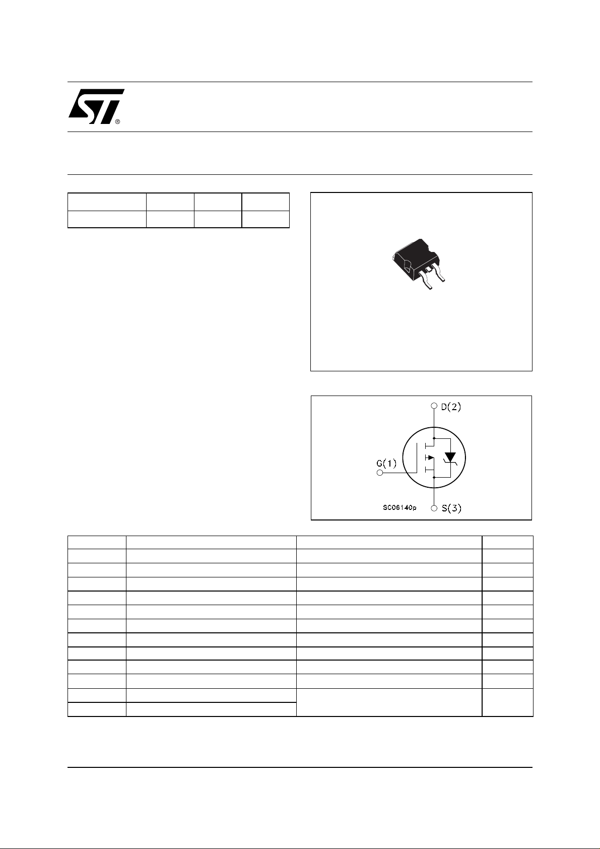
3
1
D2PAK
TO-263
(Suffix “T4”)
ADD SUFFIX “T4” FOR ORDERING IN TAPE & REEL
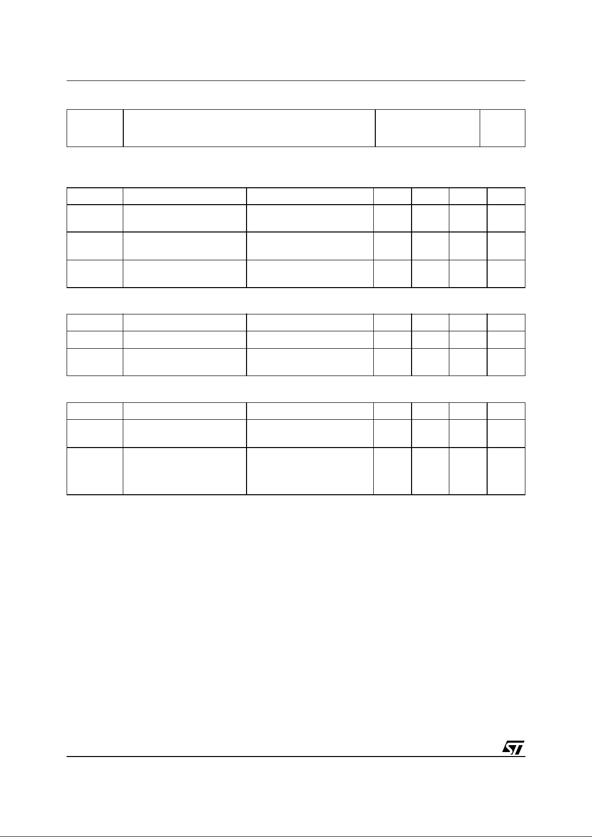
INTERNAL SCHEMATIC DIAGRAM
ABSOLUTE MAXIMUM RATINGS
Symbol Parameter Value Unit
V
DS
V
DGR
V
GS
(*) Drain Current (continuos) at T
I
D
I
D
(
I
DM
P
tot
dv/dt
E
AS
T
stg
T
j
(
Pulse widt h l i m i ted by safe op erating area
•)
(*) Curren t Lim i ted by Package
February 2002
This is preliminary information on a new product now in development or undergoing evaluation. Details are subject to change without notice.
Drain-source Voltage (VGS = 0)
Drain-gate Voltage (RGS = 20 kΩ)
55 V
55 V
Gate- source Voltage ± 16 V
= 25°C
C
Drain Current (continuos) at TC = 100°C
•)
Drain Current (pulsed) 320 A
Total Dissipation at TC = 25°C
80 A
57 A
300 W
Derating Factor 2 W/°C
(1)
Peak Diode Recovery voltage slope 7 V/ns
(2)
Single Pulse Avalanche Energy 1.4 mJ
Storage Temperature
Max. Operating Junction Temperature
Note: F or t he P- CHAN NEL MOS FE T ac tu al po la rity o f v olt ages a nd
current has to be rever sed
≤ 40A, di/dt ≤ 300A/µs , VDD ≤ V
(1) I
SD
(2) Starting Tj = 25 oC, ID = 80A, VDD = 40V
-55 to 175 °C
(BR)DSS
, Tj ≤ T
JMAX.
1/7
STB80PF55
THERMA L D ATA
Rthj-case
Rthj-amb
T
Thermal Resistance Junction-case
Thermal Resistance Junction-ambient
Maximum Lead Temperature For Soldering Purpose
l
Max
Max
Typ
0.5
62.5
300
°C/W
°C/W
°C
ELECTRICAL CHARACTERISTICS (T
= 25 °C unless otherwise specified)
case
OFF
Symbol Parameter Test Conditions Min. Typ. Max. Unit
I
V
(BR)DSS
Drain-source
= 250 µA, VGS = 0
D
55 V
Breakdown Voltage
V
= Max Rating
DS
V
= Max Rating TC = 125°C
DS
V
= ± 16 V
GS
1
10
±100 nA
ON
(*)
I
DSS
I
GSS
Zero Gate Voltage
Drain Current (V
GS
Gate-body Leakage
Current (V
DS
= 0)
= 0)
Symbol Parameter Test Conditions Min. Typ. Max. Unit
V
V
GS(th)
R
DS(on)
Gate Threshold Voltage
Static Drain-source On
= VGS ID = 250 µA
DS
V
= 10 V ID = 40 A
GS
234V
0.016 0.018
Resistance
DYNAMIC
Symbol Parameter Test Conditions Min. Typ. Max. Unit
> I
g
fs
C
iss
C
oss
C
rss
Forward Transconductance
Input Capacitance
Output Capacitance
Reverse Transfer
Capacitance
V
DS
I
D
V
DS
= 40 A
x R
D(on)
DS(on)max,
= 25V, f = 1 MHz, VGS = 0
32 S
5500
1130
600
µA
µA
Ω
pF
pF
pF
2/7
STB80PF55
ELECTRICAL CHARACTERISTICS (continued)
SWITCHING ON
Symbol Parameter Test Conditions Min. Typ. Max. Unit
t
d(on)
t
r
Q
g
Q
gs
Q
gd
(*)
Turn-on Delay Time
Rise Time
Total Gate Charge
Gate-Source Charge
Gate-Drain Charge
= 25 V ID = 40 A
V
DD
R
= 4.7 Ω VGS = 10 V
G
(Resistive Load, Figure 3)
= 25 V ID = 80 A VGS= 10V
V
DD
35
190
190
27
65
258 nC
ns
ns
nC
nC
SWITCHING OFF
(*)
Symbol Parameter Test Conditions Min. Typ. Max. Unit
t
d(off)
Turn-off Delay Time
t
f
Fall Time
V
DD
R
= 4.7 Ω V
G
GS
= 10 V
165
80
= 25 V ID = 40 A
(Resistive Load, Figure 3)
t
r(Voff)
t
t
f
c
Off-voltage Rise Time
Fall Time
Cross-over Time
SOURCE DRAIN DIODE
(*)
= 40 V ID = 80 A
V
clamp
R
= 4.7 Ω V
G
GS
= 10 V
(Inductive Load, Figure 5)
60
40
85
Symbol Parameter Test Conditions Min. Typ. Max. Unit
I
SD
I
SDM
V
SD
t
rr
Q
rr
I
RRM
(*)
Pulse width [ 300 µs, duty cycle 1.5 %.
(
•)
Pulse width limited by T
Source-drain Current
(•)
Source-drain Current (pulsed)
(*)
Forward On Voltage
Reverse Recovery Time
Reverse Recovery Charge
Reverse Recovery Current
JMAX
I
= 80 A VGS = 0
SD
= 80 A di/dt = 100A/µs
I
SD
V
= 25 V Tj = 150°C
DD
(see test circuit, Figure 5)
80
320
1.3 V
110
495
9
ns
ns
ns
ns
ns
A
A
ns
nC
A
3/7

STB80PF55
Fig. 1: Unclamped Inductive Load Test CircuitFig. 1: Unclamped Inductive Load Test Circuit Fig. 2: Unclamped Inductive Waveform
Fig. 3: Switching Times Test Circuits For Resistive
Load
Fig. 5: Test Circuit For Inductive Load Switching
And Diode Recovery Times
Fig. 4: Gate Charge test Circuit
4/7

D2PAK MECHANICAL DATA
STB80PF55
DIM.
A 4.4 4.6 0.173 0.181
A1 2.49 2.69 0.098
A2 0.03 0.23 0.001 0.009
B 0.7 0.93 0.028 0.037
B2 1.14 1.7 0.045 0.067
C 0.45 0.6 0.018 0.024
C2 1.21 1.36 0.048 0.054
D 8.95 9.35 0.352 0.368
D1 8 0.315
E 10 10.4 0.394 0.409
E1 8.5 0.334
G 4.88 5.28 0.192 0.208
L 15 15.85 0.591 0.624
L2 1.27 1.4 0.050 0.055
L3 1.4 1.75 0.055 0.069
M 2.4 3.2 0.094 0.126
R 0.4 0.016
V2 0° 8° 0° 8°
MIN. TYP. MAX. MIN. TYP. TYP.
mm. inch.
0.106
5/7

STB80PF55
D2PAK FOOTPRINT
TAPE AND REEL SHIPMENT (suffix ”T4”)*
TUBE SHIPMENT (no suffix)*
REEL MECHANICAL DATA
DIM.
A 330 12.992
B 1.5 0.059
C 12.8 13.2 0.504 0.520
D 20.2 0.795
G 24.4 26.4 0.960 1.039
N 100 3.937
T 30.4 1.197
mm inch
MIN. MAX. MIN. MAX.
TAPE MECHANICAL DATA
DIM.
A0 10.5 10.7 0.413 0.421
B0 15.7 15.9 0.618 0.626
D 1.5 1.6 0.059 0.063
D1 1.59 1.61 0.062 0.063
E 1.65 1.85 0.065 0.073
F 11.4 11.6 0.449 0.456
K0 4.8 5.0 0.189 0.197
P0 3.9 4.1 0.153 0.161
P1 11.9 12.1 0.468 0.476
P2 1.9 2.1 0075 0.082
R50 1.574
T0.25 0.35 .0.0098 0.0137
W 23.7 24.3 0.933 0.956
mm inch
MIN. MAX. MIN. MAX.
* on sales type
6/7
BASE QTY BULK QTY
1000 1000

STB80PF55
Information furnished is believed to be ac curate and reli able. Howev er, STMicroel ectronics assumes no responsibilit y for the consequence s
of use of such information nor for any infringement of patents or other rights of third parties which may result from its use. No license is granted
by implic ation or otherwise under any patent or patent rights of STMi croelectr onics. Specifications mentioned in thi s publicati on are subject
to change without notice. This publication supersedes and replaces all information previously supplied. STMicroelectronics products are not
authorized for use as cri tical comp onents in life support dev i ces or systems wi t hout express written ap proval of STMi croelect ro nics.
The ST log o i s registered trademark of STMicroelectronics
2002 STMi croelectr oni cs - All Rights Reserved
All other names are the property of their respective owners.
Australi a - Brazil - Canada - Chin a - F i nl and - Franc e - Germany - Hong Kong - Ind i a - Is rael - Ital y - J apan - Malaysia - Malt a - Morocco -
Singapor e - S pai n - Sweden - Swi tzerland - United Kingdom - United S tates.
STMicroelect ro n ics GRO UP OF COMPANI ES
http://www.st.com
7/7
 Loading...