

SGS Thomson Microelectronics ST750ACN, ST750ACD-TR, ST750ACD, ST750ABN, ST750ABD-TR Datasheet
...
CURRENT-MODE PWM DC-DC CONVERTERS
■ UP TO 450mA LOAD CURRENTS
■ 200kHz HIGH-FREQUENCY
CURRENT-MODE PWM
■ 85% TO 96% EFFICIENCIES
■ 33µHOR100µH PRE-SELECTED
INDUCTOR VALUE, NO COMPONENT
DESIGN REQUIRED
■ 0.8mA QUIESCENT CURRENT
■ 0.3µA SHUTDOWN SUPPLY CURRENT
■ ADJUSTABLE OUTPUT VOLTAGE
■ OVERCURRENT, SOFT-START AND
UNDERVOLTAGE LOCKOUT PROTECTION
■ CYCLE-BY-CYCLE CURRENT LIMITING
■ PACKAGE AVAILABLE : DIP- 8 AND SO - 8
DESCRIPTION
The ST750A is an adjustable output CMOS,
step-down switching regulator. The ST750A
accepts inputs between 4V and 1 1V and delivers
450mA. Typical efficiencies are 85% to 96%.
Quiescent supply current is 0.8mA and only 0.3µA
in shutdown mode. The output does not exhibit
frequency over th is specified range. Pulse-width
modulation (PWM) current-mode control provides
ST750A
ADJUSTABLE STEP-DOWN,
DIP-8 SO-8
precise output regulation and excellent transient
responses. Output voltage accuracy is
guaranteed to be ±4.5% plus feedback resistor
tolerance over line, load, and temperature
varations.
Fixed-frequency switching and absenc e of
subharmonic ruipple allows easy filtering of output
ripple and noise, as well as the use of smal l
external components. This regul ators requi re o nly
a s ingle inductor value to work in most
applications, so no inductor design is necessary.
Typical applications are: Cellular phones & radios,
portable Instruments, Porta ble Communications
Equipments and Computer Peripherals.
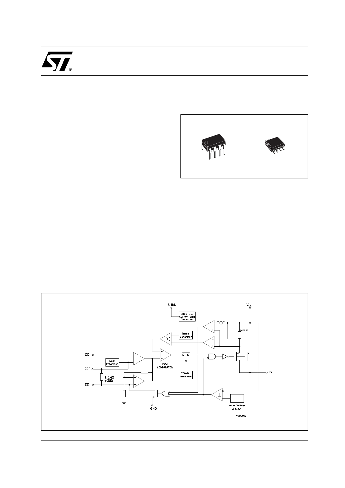
SCHEMATIC DIAGRAM
1/9January 2003

ST750A
ABSOLUTE MAXIMUM RATINGS
Symbol Parameter² Value Unit
V
V
V
SHDN
V
S,VC
I
LX
I
REF
P
TOT
T
T
Absolute Maximum Ratings are those values beyond which damage to the device may occur. Functional operation under these condition is
not implied.
THERMAL DATA
Symbol Parameter SO-8 DIP-8 Unit
R
thj-amb
(*) This value depends from thermal design of PCB on which the device is mounted.
DC Input Voltage
CC
Switch Pin Voltage -0.3 to (VCC+ 0.3)
LX
Shutdown Voltage (SHDN) -0.3 to (VCC+ 0.3)
Soft Start (SS) and Compensation Capacitor (CC) Pins Voltage -0.3 to (VCC+ 0.3)
Switching Peak Current
Reference Current
Continuous Power Dissipation at TA=70°C (DIP-8)
(SO-8)
Storage Temperature Range
stg
Operating Junction Temperature Range (C series)
op
Thermal Resistance Junction-ambient (*)
(B series)
160 100 °C/W
-0.3 to 12 V
V
V
V
2A
2.5 mA
550
344
mW
mW
-40 to +150 °C
0to+70
-40 to +85
°C
°C
ORDERING CODES
TYPE DIP8 SO-8 SO-8 (T&R)
ST750AB ST750ABN ST750ABD ST750ABD-TR
ST750AC ST750ACN ST750ACD ST750ACD-TR
2/9

CONNECTION DIAGRAM (top view)
PIN DESCRIPTION
Pin N° Symbol Name and Function
1 SHDN
2 REF Reference Output Voltage: (1.25V): Bypass to GND with a capacitor that does not
3 SS Soft Start: a capacitor between SS and GND provides soft-start and short-circuit
4 CC Compensation Capacitor Input: externally compensates the outer (voltage)
5 IC Internal Connection: make no external connection to this pin
6 GND Ground
7 LX Switch Output. Drain of internal P-Channel Power MOSFET
8V
CC
Shutdown control (active low): If connected to GND the IC is in shutdown.
Connect to V
for normal operation (ON MODE)
CC
exceed 47nF
protections.
feedback loop. Connect to OUT with 330pF capacitor
Supply Voltage Input. Bypass to GND with 1µF ceramic capacitance and large
value electrolytic capacitor in parallel. The 1µF capacitor must be as close as
possible to the GND and V
CC
pins
ST750A
3/9
 Loading...