

SGS Thomson Microelectronics ST735CN, ST735CD, ST735CD-TR Datasheet
-5V INVERTING, NEGATIVE OUTPUT
CURRENT-MODE PWM REGULATOR
■ CONVERTS +4.0V TO + 6.2V INPUT TO -5V
OUTPUT
■ 1W GUARANTEEDOUTPUT POWER
■ 75% TYPICAL EFFICIENCY
■ 0.8mA QUIESCENT CURRENT
■ 10µA SHUTDOWN MODE
■ 160KHZ FIXED FREQUENCY OSCILLATOR
■ CURRENT MODE PWM CONVERTER
■ LOW NOISE AND JITTER
■ SOFT START
■ SIMPLE APPLICATION CIRCUIT
■ UNDERVOLTAGE LOCKOUT
DESCRIPTION
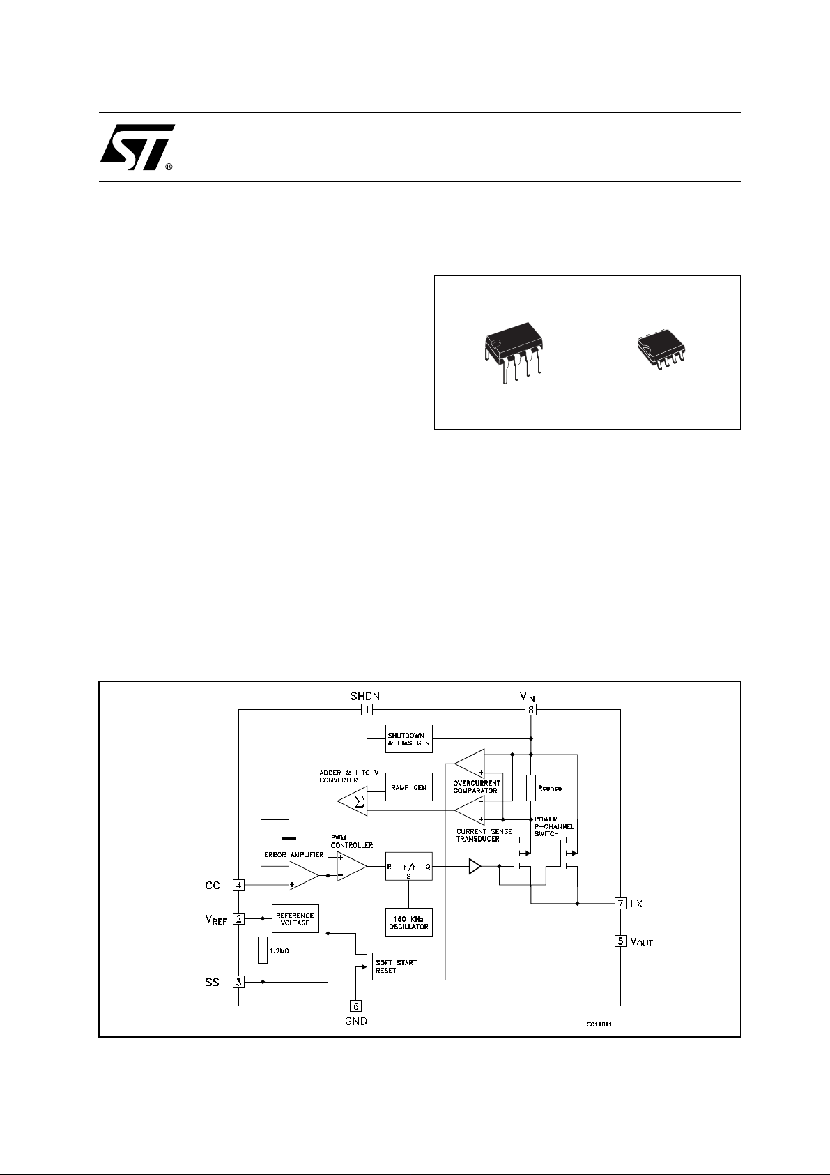
The ST735 is a Bi-CMOS, inverting s w itch mode
DC-DC regulator with internal Power MOSFE T's
that generates a fixed -5V output voltage from a
4V to 6.2V input voltage; is guaranteed an output
current of 200mA for inputs great er than 4.5V . The
quiescent current for this device is typically of
0.8mA and, in shutdown mode it is reduced to
10µA.
ST735
DIP-8 SO-8
These power-conserving features, along with hi gh
efficiency and applications circuits, t hat lend itself
to minaturization, make the ST735 excellent in a
broad range of on-card, HDD and portable
equipment applications. The ST735 employ a
high performance current mode puls e with
modulation (PWM) control scheme to provide tight
output voltage regulat ion and low noise. T he
fixed frequency oscillator is factory trimmed to
160KHz, allowing for easy noise filtering. T he
regulator in production is tested to guarantee an
output accuracy within ±5% over all specified
conditions.
SCHEMATIC DIAGRAM
1/9August 2002
ST735
ABSOLUTE MAXIMUM RATINGS
Symbol Parameter Value Unit
V
SHDN
V
V
V
OUT
I
LX
P
T
T
Absolute Maximum Ratings are those values beyond which damage to the device may occur. Functional operation under these condition is
not implied.
THERMAL DATA
Symbol Parameter DIP-8 SO-8 Unit
R
thj-case
DC Input Voltage (VINto GND)
IN
Shutdown Voltage (SHDN to GND) -0.3 to V
Switch Voltage (Lx to VIN)
LX
Feedback Voltage (V
FB
Output Voltage (V
OUT
to GND)
OUT
to GND)
Other Input Voltage (SS, CC to GND) -0.3 to V
Peack Switch Current
Power Dissipation at Tj= 70°C DIP-8 725
tot
Storage Temperature Range
stg
Operating Junction Temperature Range
op
Thermal Resistance Junction-case
SO-8 470
2 8 °C/W
-0.3 to +7 V
+0.3
+
V
-12.5 to +0.3 V
-11to+0.3 V
-11to+0.3 V
+0.3
+
V
2A
mW
-55 to +150 °C
-40 to +125 °C
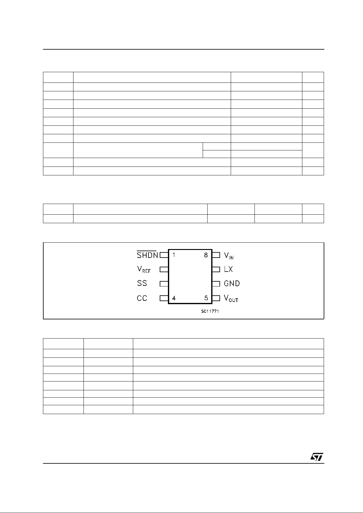
CONNECTION DIAGRAM (t op v iew)
PIN DESCRIPTION
Pin N° Symbol Name and Function
1 SHDN SHUT-DOWN Control (VCC=ON GND=Shutdown
2V
REF
3 SS Soft Start
4 CC Compensation Input
5V
OUT
6 GND Ground
7 LX Switch Output
8V
IN
Reference Output Voltage
Negative Output Voltage
Positive Supply - Voltage Input
2/9
ORDERING CODES
TYPE DIP-8 SO-8 SO-8 (T&R)
ST735 ST735CN ST735CD ST735CD-TR
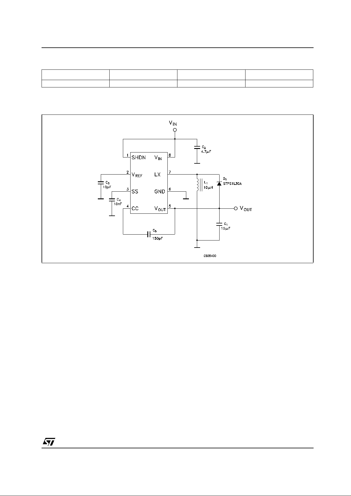
TYPICAL APPLICATION CIRCUIT
ST735
NOTE:
1) All capacitors are X7R ceramic
2) C
can be omitted if are used higher values for the input and output capacitors C2=47µF, C1=100pF.
5
3/9
 Loading...