

SGS Thomson Microelectronics ST72T91L, ST7291L6, ST7291L5A, ST7291L5, ST7291L4 Datasheet
...
December 1997 1/5
Thisispreliminaryinformation ona newproductin development orundergoingevaluation. Detailsaresubject to change without notice.
R
ST7291L
8-BIT MCU WITH 8/12/16/24/32K ROM, TIMER, SUPPLY
SUPERVISOR AND CARRIER FREQUENCY GENERATOR
BRIEF DATA
■ 2 to 5.5V Supply Operating Range
■ 8MHz Maximum Clock Frequency
■
Fully Static Operation
■
0to+70°C Operating Temperature Range
■ Run, Wait, Stop and RAM Retention modes
■ User ROM: 12/16/24/32 Kbytes
■
Data RAM: 256/384 bytes
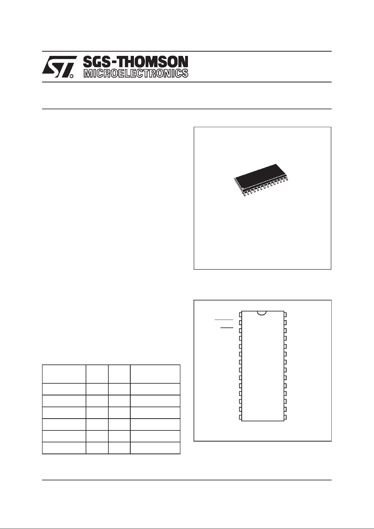
■ 28 pin SO Plastic Packages
■ 21 Bidirectional I/O lines
■ 8 standard Push-pull I/Os with wake-up feature
13 standard Push-pull I/Os
■ 16-bit Timer with Output Compare (no output
pin)
■
Low Voltage Detector (LVD)
■
Interrupt Wake-up function
■ IR Carrier Frequency Generator
■ 8-bit Data Manipulation
■
63 Basic Instructions
■ 17 main Addressing Modes
■ 8x8 Unsigned Multiply instruction
■ True Bit Manipulation
■
Complete Development Support on PC/DOS/
Windows 3.1x/95/NT with Real-Time Emulator
■ Full Software Package (Cross-Assembler,
Debugger)
■
Full Hardware Emulator
■ EPROM and OTP support
DEVICE SUMMARY
Note 1. This device is in development, consult your
SGS-THOMSON representative for the current status.
Figure 1. Pin Description
Notes:
1. PC1 on ST7291L2/L3/L4; software selectable as OP on
ST7291L6/L5/L5A
DEVICE
ROM
(Bytes)
RAM
(Bytes)
CARRIER
GENERATOR
ST7291L6
(1)
32K 384 Yes
ST7291L5 24K 384 Yes
ST7291L5A 16K 384 Yes
ST7291L4 16K 256 No
ST7291L3 12K 256 No
ST7291L2 8K 256 No
PSO28
(See end of Datasheet for Ordering Information)
1
2
3
4
5
6
7
8
9
10
11
12
13
14
15
16
17
18
19
20
V
DD
RESET
WKP
PA7
PA6
PA1
PC0
PA5
PA4
PA3
OSCin
OSCout
PC1/OP
(1)
PC6
PC7
PB6
PB5
PB4
PB3
PB2
28
27
26
25
24
23
22
21
PA2
PA0
PB0
PB1
V
SS
TEST
PC5
PB7
1
2/5
ST7291L
1 GENERAL DESCRIPTION
1.1 INTRODUCTION
The ST7291L CMOS Microcontroller Unit is a
member of the ST7 family of microcontrollers. The
device is based on an industry-standard 8-bit core
and features an enhanced instruction set. Oscillator frequency may be as high as 8MHz, however,
thanks to the fully static design, operation is possible down to DC. Under software control, the
ST7291L may be placed in either WAIT or HALT
modes, thus reducing power consumption.
The enhanced instruction set and addressing
modes afford real programming potential. In addition to standard 8-bit data management, the
ST7291L features bit manipulation, 8x8 unsigned
multiplication and indirect addressing modes.
The device includes a CPU, ROM, RAM, I/O, an
on-chip oscillator, a timer with output compare
system and, depending on theversion, aLow Voltage Detection (LVD) and Carrier Frequency generation for remote control applications.
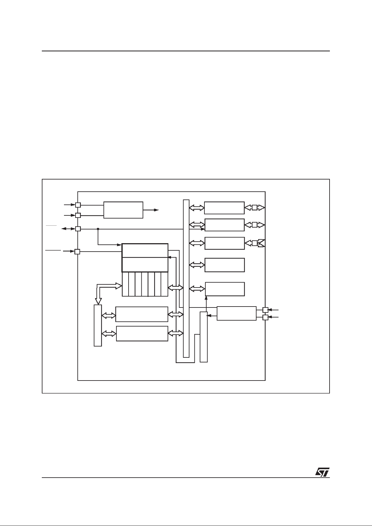
Figure 2. ST7291L Block Diagram
OSCILLATOR
ADDRESS BUS
PORT A
PORT B
CARRIER FREQ.
8 BIT CORE
PA0..PA7 (8-bit)
PB0..PB7 (8-bit)
PC0, PC1, PC6, PC7
PORT C
V
DD
LOW VOLTAGE
DETECTOR
TIMER
SYSTEM
V
PP
PC5
PCL
PCH
SP
XYA
CC
CONTROL
Internal
CLOCK
ROM
8K/12K/16K/24K/32K
RAM
256/384
GENERATOR
OSCout
OSCin
WKP
RESET
DATA BUS
 Loading...