

SGS Thomson Microelectronics ST3243ECTR, ST3243ECPR, ST3243ECDR, ST3243ECD, ST3243EBTR Datasheet
...
±15KV ESD PROTECTED 3 TO 5.5V, 400KBPS,
RS-232 TRANSCEIVER WITH AUTO-POWERDOWN
■ ESD PROTECTION FOR RS-232 I/O PINS:
±8KV IEC 1000-4-2 CONTACT DISCHARGE
±15KV HUMAN BODY MODEL
■ 1µA SUPPLY CURRENT ACHIEVED WHEN
IN AUTO-POWERDOWN
■ 250Kbps MINIMUM GUARANTEED DATA
RATE
■ GUARANTEED 6V/µsSLEWRATERANGE
■ GUARANTEED MOUSE DRIVEABILITY
■ 0.1µF EXTERNAL CAPACITORS
■ MEET EIA/TIA-232SPECIFICATIONSDOWN
TO 3V
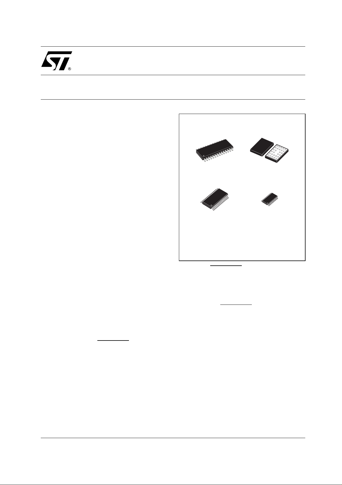
■ AVAILABLEIN SO-28, SSOP-28, TSSOP28
AND FLIP-CHIP28 PACKAGES
SOP
ST3243E
Flip-Chip28
DESCRIPTION
The ST3243E device consists of 3 drivers, 5
receivers and a dual charge-pump circuit. The
device meets the requirements of EIA/TIA and
V.28/V.24 comunication standards providing high
data rate capability and enhanced electrostatic
discharge (ESD) protection. All trans mi tter outputs
and receiver input are protected to ±8KV USING
IEC 1000-4-2 contact discharg e and ±15KV using
the H uman Body Model. The receiver R2 is
always act ive to implement a wake-up feature for
serial port.
The ST3243 E has a proprietary low-dropout
transmitter output stage enabling true RS-232
performance from a 3.0V to 5.5V supply with a
dual charge p ump. The device is guarant eed to
run at data rates of 250kbps while maintaining
RS-232 output levels.
The Auto-powerdown feature functions when
FORCEON is low and FORCEOFF
is high. During
this mode of operation, if the device does not
sense a valid RS-232 signal, the driver outputs are
SSOP
disabled. If FORCEOFF
TSSOP
is set low, both drivers
and receivers (expert R2B) are shut off, a nd
supply current is reduced to 1µA. Discon nec ting
the serial port or turning off the peripheral drives
causes the auto-powerdown condition to occur.
Auto-powerdown can be disabled when
FORCEON and FORCEOFF
are high, and should
be done when driving a serial mouse. With
Auto-powerdown enabled, the device is activated
automatically when a valid signal is applied to any
receiverinput.
Typical application are in notebook, subnotebook,
palmtop computers, battery-powered equipme nt,
hand-held equipment, peripherals and printers.
1/14January 2003
ST3243E
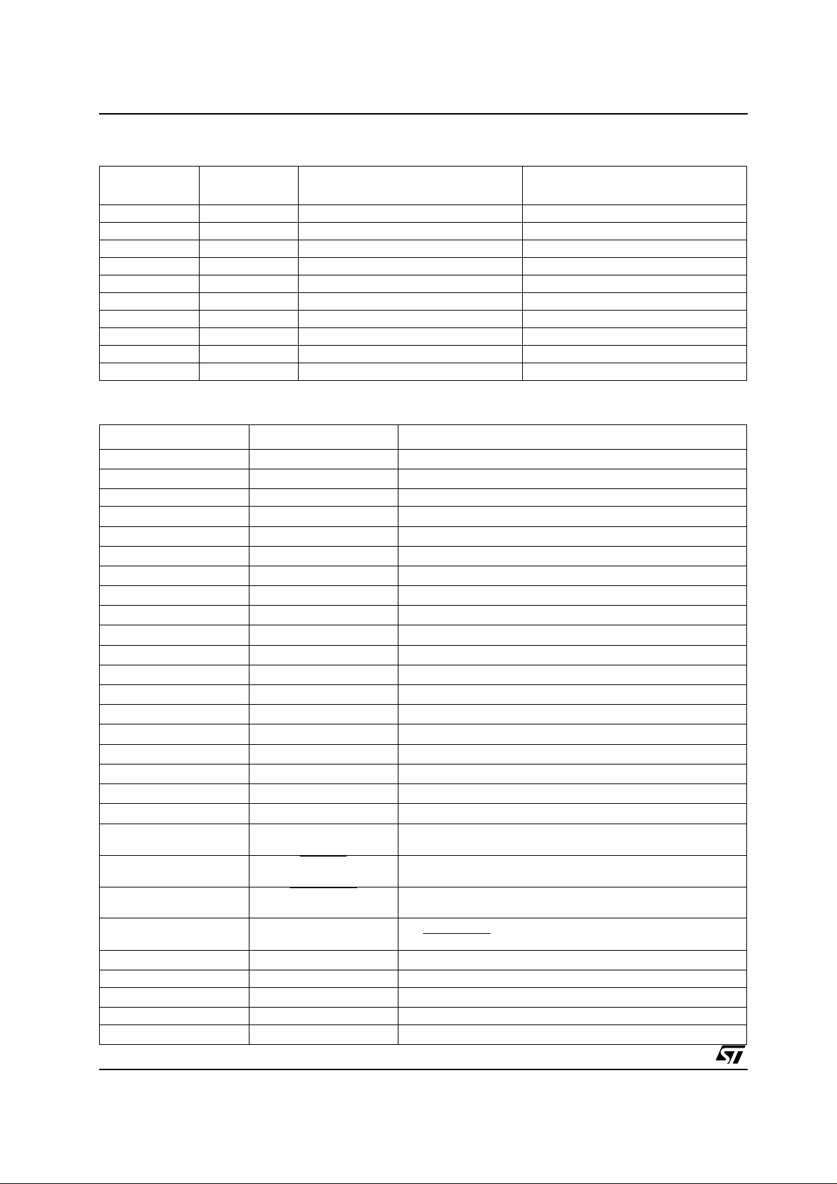
ORDERING CODES
Type
Temperature
Range
Package Comments
ST3243ECD 0 to 70 °C SO-28 (Tube) 27parts per tube / 12tube per box
ST3243EBD -40 to 85 °C SO-28 (Tube) 27parts per tube / 12tube per box
ST3243ECDR 0 to 70 °C SO-28 (Tape & Reel) 1000 parts per reel
ST3243EBDR -40 to 85 °C SO-28 (Tape & Reel) 1000 parts per reel
ST3243ECPR 0 to 70 °C SSOP-28 (Tape & Reel) 1350 parts per reel
ST3243EBPR -40 to 85 °C SSOP-28 (Tape & Reel) 1350 parts per reel
ST3243ECTR 0 to 70 °C TSSOP28 (Tape & Reel) 2500 parts per reel
ST3243EBTR -40 to 85 °C TSSOP28 (Tape & Reel) 2500 parts per reel
ST3243ECJ 0 to 70 °C FLIP-CHIP28 coming soon
ST3243EBJ -40 to 85 °C FLIP-CHIP28 coming soon
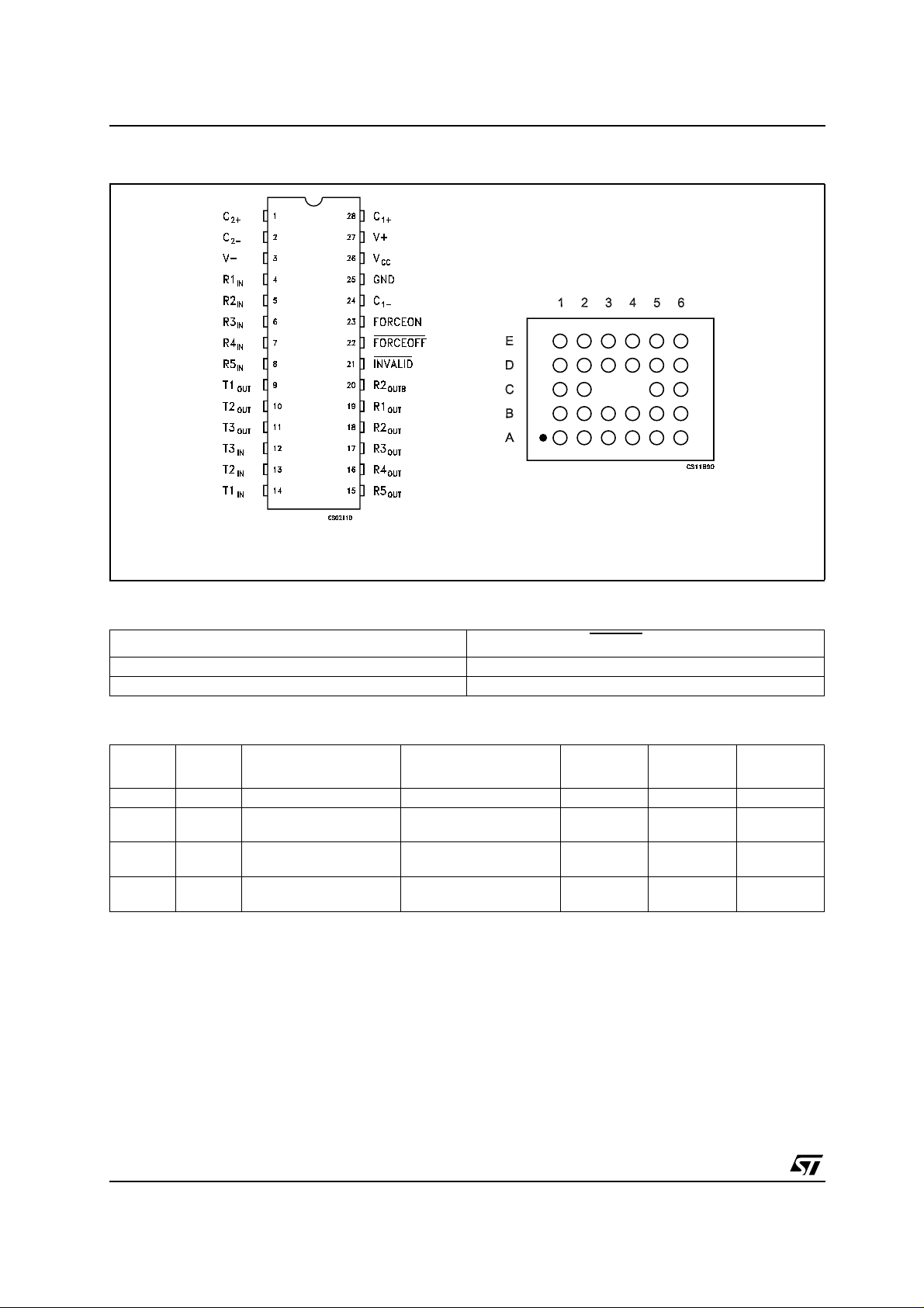
PIN DESCRIPTION
PlN N° SYMBOL NAME AND FUNCTION
1C
2C
3 V- -5.5V Generated by the Charge Pump
4R1
5R2
6R3
7R4
8R5
9T1
10 T2
11 T3
12 T3
13 T2
14 T1
15 R5
16 R4
17 R3
18 R2
19 R1
20
21 INVALID
22 FORCEOFF
23 FORCEON Drive high to override automatic circuitry keeping transmitters
24 C
25 GND Ground
26 V
27 V+ 5.5V Generated by the Charge Pump
28 C
2/14
+ Positive Terminal of Inverting Charge Pump Capacitor
2
- Negative Terminal of Inverting Charge Pump Capacitor
2
First Receiver Input Voltage
Second Receiver Input Voltage
Third Receiver Input Voltage
Fourth Receiver Input Voltage
Fifth Receiver Input Voltage
First Transmitter Output Voltage
Second Transmitter Output Voltage
Third Transmitter Output Voltage
Third Transmitter Input Voltage
Second Transmitter Input Voltage
First Transmitter Input Voltage
Fifth Receiver Output Voltage
Fourth Receiver Output Voltage
Third Receiver Output Voltage
Second Receiver Output Voltage
First Receiver Output Voltage
Non-inverting Complementary Receiver Output, always active
for wake-up
R2
IN
IN
IN
IN
IN
OUT
OUT
OUT
IN
IN
IN
OUT
OUT
OUT
OUT
OUT
OUTB
Output of the valid signal detector. Indicates if a valid RS-232
level is present on receiver inputs logic "1"
Drive low to shut down transmitters and on-board power
supply. This over-rides all automatic circuitry and FORCEON
on (FORCEOFF
- Negative Terminal of Voltage- Charge Pump Capacitor
1
CC
+ Positive Terminal of Voltage- Charge Pump Capacitor
1
Supply Voltage
must be high)

PIN DESCRIPTION
PlN N° SYMBOL NAME AND FUNCTION
A1 R2
A2 R3
A3 R4
A4 R5
A5 T1
A6 T2
B1 V- -5.5V Generated by the Charge Pump
B2 R1
B3 T3
B4 T3
B5 T1
B6 T2
C1 C
C2 C
C5 R4
C6 R5
D1 C
D2 V+ 5.5V Generated by the Charge Pump
D3 V
D4 FORCEON Drive high to override automatic circuitry keeping transmitters
D5 R1
D6 R3
E1 GND Ground
E2 C
E3 FORCEOFF
E4 INVALID
E5
E6 R2
IN
IN
IN
IN
OUT
OUT
IN
OUT
IN
IN
IN
+ Positive Terminal of Inverting Charge Pump Capacitor
2
- Negative Terminal of Inverting Charge Pump Capacitor
2
OUT
OUT
+ Positive Terminal of Voltage- Charge Pump Capacitor
1
CC
OUT
OUT
- Negative Terminal of Voltage- Charge Pump Capacitor
1
Second Receiver Input Voltage
Third Receiver Input Voltage
Fourth Receiver Input Voltage
Fifth Receiver Input Voltage
First Transmitter Output Voltage
Second Transmitter Output Voltage
First Receiver Input Voltage
Third Transmitter Output Voltage
Third Transmitter Input Voltage
First Transmitter Input Voltage
Second Transmitter Input Voltage
Fourth Receiver Output Voltage
Fifth Receiver Output Voltage
Supply Voltage
on (FORCEOFF
must be high)
First Receiver Output Voltage
Third Receiver Output Voltage
Drive low to shut down transmitters and on-board power
supply. This over-rides all automatic circuitry and FORCEON
Output of the valid signal detector. Indicates if a valid RS-232
level is present on receiver inputs logic "1"
R2
OUTB
OUT
Non-inverting Complementary Receiver Output, always active
for wake-up
Second Receiver Output Voltage
ST3243E
3/14
ST3243E
PIN CONFIGURATION
SOP, SSOP, TSSOP
(top view)
FLIP-CHIP 6x5
(bottom view, bumps side)
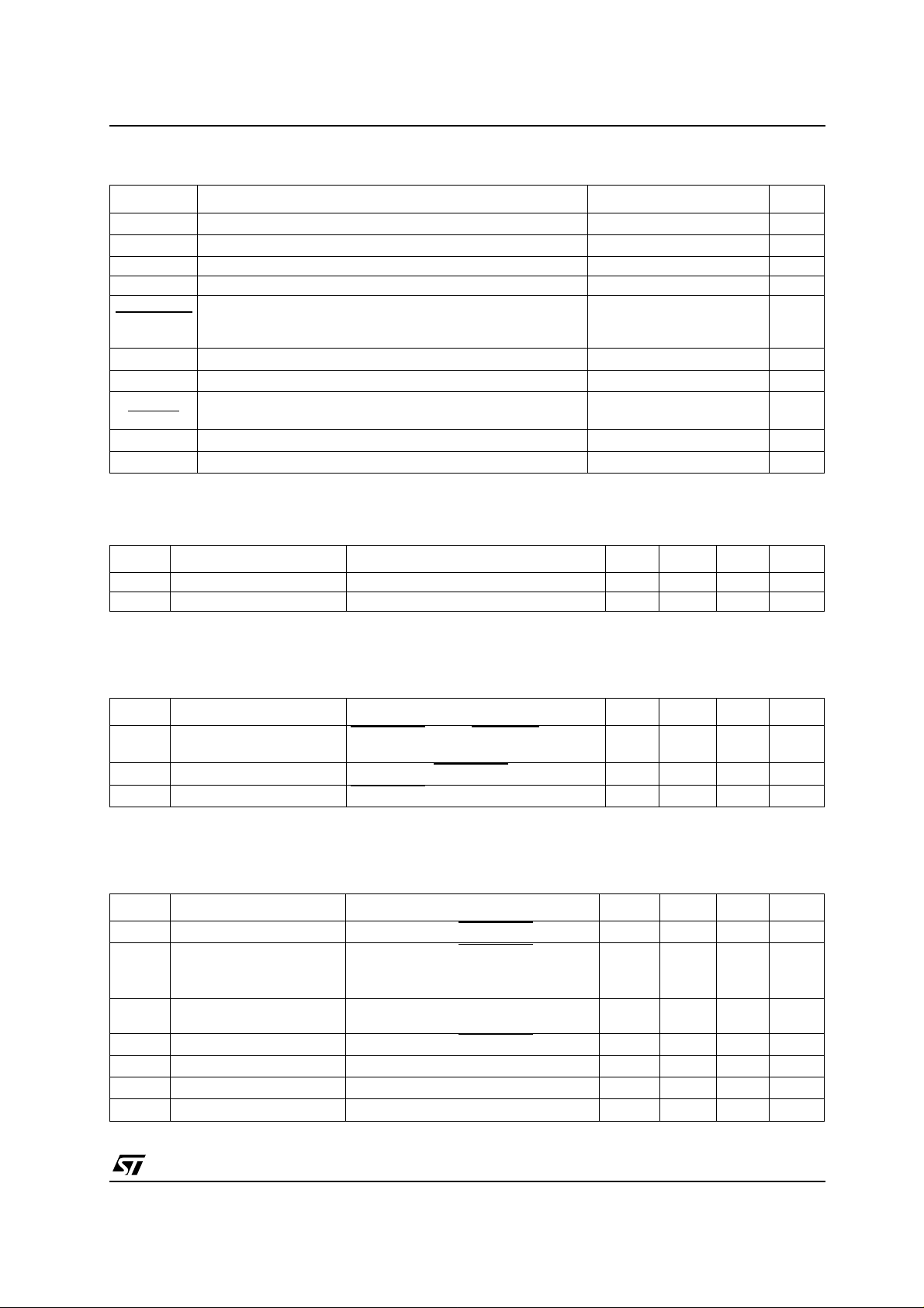
INVALID TRUTH TABLE
RS-232 SIGNAL PRESENT AT ANY RECEIVER INPUT INVALID OUTPUT
YES H
NO L
OUTPUT CONTROL TRUTH TABLE
FORCEONFORCE
OFF
X 0 X Shutdown (Force OFF) HIGH Z HIGH Z ACTIVE
11 X
01 YES
01 NO
VALID RECEIVER
LEVEL
OPERATION STATUS
Normal Operating (Force
ON)
Normal Operating
(Auto-powerdown)
Shutdown (Auto-power-
down)
T
OUT
ACTIVE ACTIVE ACTIVE
ACTIVE ACTIVE ACTIVE
HIGH Z ACTIVE ACTIVE
R
OUT
R
2OUTB
4/14
ST3243E
ABSOLUTE MAXIMUM RATINGS
Symbol Parameter Value Unit
V
CC
V+
V- Inverted Voltage Terminal 0.3 to -7 V
V+ +|V-| 13 V
FORCEON,
FORCEOFF,
T
IN
R
IN
T
OUT
R
OUTROUTB
INVALID
t
SHORT
T
stg
Absolute Maximum Ratings are those values beyond which damage to the device may occur. Functional operation under these condition is
not implied.
ESD PERFORMANCE: T RANSMITTER OUTPUTS, RECEIVER INPUTS
Symbol Parameter Test Conditions Min. Typ. Max. Unit
ESD ESD Protection Voltage Human Body Model ± 15 KV
ESD ESD Protection Voltage IEC 1000-4-2 (Contact Discharge) ± 8KV
Supply Voltage -0.3 to 6
Doubled Voltage Terminal (V
-0.3) to 7
CC
Input Voltage -0.3 to 6
Receiver Input Voltage Range ± 25
Transmitter Output Voltage Range ± 13.2
Receiver Output Voltage Range -0.3 to (VCC+ 0.3)
Short Circuit Duration on T
(one at a time) Continuous
OUT
Storage Temperature Range -65 to 150
V
V
V
V
V
V
°C
ELECTRICAL CHARACTERISTICS
(C
Typical values are referred to T
Symbol Parameter Test Conditions Min. Typ. Max. Unit
I
I
SUPPLY
=0.1µF, VCC=3Vto5.5V,TA= -40 to 85°C, unles s otherwise specified.
1-C4
=25°C)
A
ASHDN
I
SHDN
Supply Current
Auto-powerdown
Supply Current FORCEON = FORCEOFF =V
Shutdown Supply Current FORCEOFF =GND 1 10 µA
FORCEOFF = GNDFORCEON =V
All R_IN open or grounded
CC
CC
110µA
0.3 1 mA
LOGIC INPUT ELECTRICAL CHARACTERISTICS
(C
Typical values are referred to T
Symbol Parameter Test Conditions Min. Typ. Max. Unit
V
=0.1µF, VCC=3Vto5.5V,TA= -40 to 85°C, unles s otherwise specified.
1-C4
V
TIL
V
TIH
THYS
I
IL
I
OL
V
OL
V
OH
Input Logic Threshold Low T-IN, FORCEON, FORCEOFF 0.8 V
Input Logic Threshold High T-IN, FORCEON, FORCEOFF
Transmitter Input
Hysteresis
Input Leakage Current T-IN, FORCEON, FORCEOFF ± 0.01 ± 1.0 µA
Output Leakage Current Receiver Disabled ± 0.05 ± 10 µA
Output Voltage Low I
Output Voltage High I
=25°C)
A
VCC= 3.3V
V
OUT
OUT
=5V
CC
= 1.6mA 0.4 V
= -1mA VCC-0.6 VCC-0.1 V
2
2.4
0.5 V
V
V
5/14
 Loading...