

SGS Thomson Microelectronics ST3241ECTR, ST3241ECPR, ST3241ECDR, ST3241ECD, ST3241EBTR Datasheet
...
1/10October 2002
■ ESD PROTECTION FOR RS-232 I/O PINS:
±8KV IEC 1000-4-2 CONTACT DISCHARGE
±15KV HUMAN BODY MODEL
■ 1µA SUPPLY CURRENT ACHIEVED WHEN
IN AUTO-POWERDOWN
■ 250Kbps MINIMUM GUARANTEED DATA
RATE
■ GUARANTEED 6V/µsSLEWRATERANGE
■ GUARANTEED MOUSE DRIVEABILITY
■ 0.1µF EXTERNAL CAPACITORS
■ MEET EIA/TIA-232SPECIFICATIONSDOWN
TO 3V
■ AVAILABLEIN SO-28, SSOP28 AND
TSSOP28 PACKAGES
DESCRIPTION
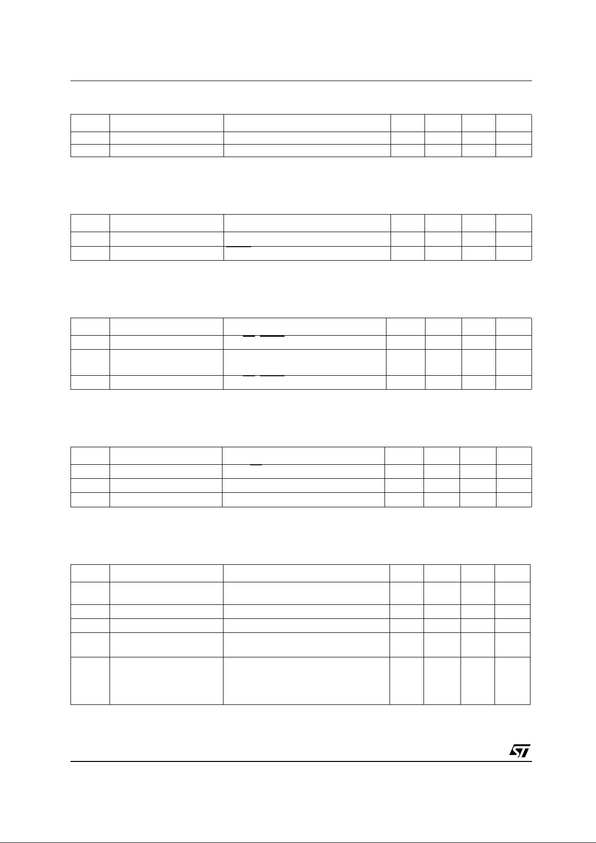
The ST3241E device consists of 3 drivers, 5
receivers and a dual charge-pump circuit. The
device meets the requirements of EIA/TIA and
V.28/V.24 comunication standards providing high
data rate capability and enhanced electrostatic
discharge (ESD) protection. All trans mi tter outputs
and receiver input are protected to ±8KV USING
IEC 1000-4-2 contact discharg e and ±15KV using
the H uman B ody Model. The receiver R2 is
always act ive to implement a wake-up feature for
serial port.
The ST3241 E has a proprietary low-dropout
transmitter output stage enabling true RS-232
performance from a 3.0V to 5.5V supply with a
dual charge pump. The device is guaranteed to
run at data rates of 250kbps while maintaining
RS-232 output levels.
It is a complete serial port (3 drivers, 5 receivers)
intended for notebook or subnotebook compute rs.
Receivers R1 and R2 hav e extra out puts in
addition to t heir standard outputs. These ex tra
outputaare always active.
Typical application are in notebook, subnotebook,
palmtop computers, battery-powered equipment,
hand-held equipment, peripherals and printers.
ST3241E
±15KV ESD PROTECTED 3 TO 5.5V, 400KBPS,
RS-232 TRANSCEIVER WITH AUTO-POWERDOWN
SSOP
SOP
TSSOP
ST3241E
2/10
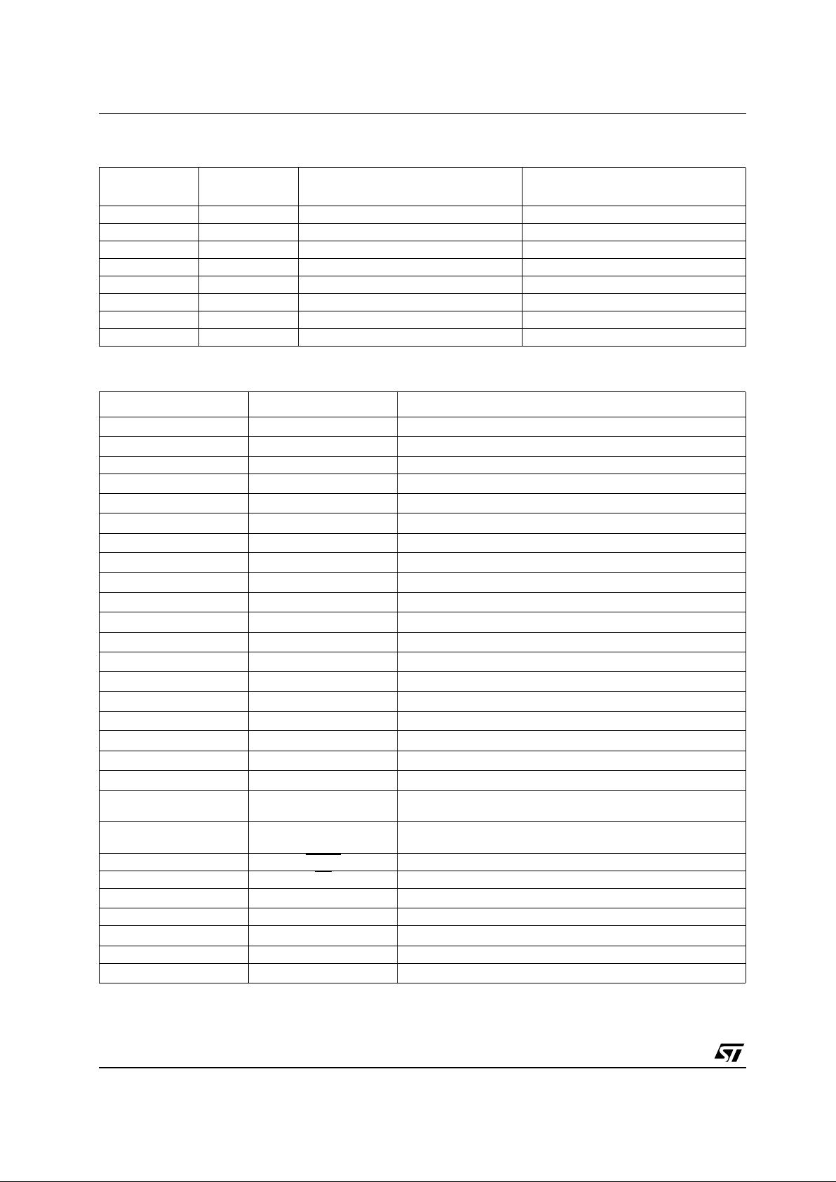
ORDERING CODES
PIN DESCRIPTION
Type
Temperature
Range
Package Comments
ST3241ECD 0 to 70 °C SO-28 (Tube) 27parts per tube / 12tube per box
ST3241EBD -40 to 85 °C SO-28 (Tube) 27parts per tube / 12tube per box
ST3241ECDR 0 to 70 °C SO-28 (Tape & Reel) 1000 parts per reel
ST3241EBDR -40 to 85 °C SO-28 (Tape & Reel) 1000 parts per reel
ST3241ECPR 0 to 70 °C SSOP-28 (Tape & Reel) 1350 parts per reel
ST3241EBPR -40 to 85 °C SSOP-28 (Tape & Reel) 1350 parts per reel
ST3241ECTR 0 to 70 °C TSSOP28 (Tape & Reel) 2500 parts per reel
ST3241EBTR -40 to 85 °C TSSOP28 (Tape & Reel) 2500 parts per reel
PlN N° SYMBOL NAME AND FUNCTION
1C
2
+ Positive Terminal of Inverting Charge Pump Capacitor
2C
2
- Negative Terminal of Inverting Charge Pump Capacitor
3 V- -5.5V Generated by the Charge Pump
4R1
IN
First Receiver Input Voltage
5R2
IN
Second Receiver Input Voltage
6R3
IN
Third Receiver Input Voltage
7R4
IN
Fourth Receiver Input Voltage
8R5
IN
Fifth Receiver Input Voltage
9T1
OUT
First Transmitter Output Voltage
10 T2
OUT
Second Transmitter Output Voltage
11 T3
OUT
Third Transmitter Output Voltage
12 T3
IN
Third Transmitter Input Voltage
13 T2
IN
Second Transmitter Input Voltage
14 T1
IN
First Transmitter Input Voltage
15 R5
OUT
Fifth Receiver Output Voltage
16 R4
OUT
Fourth Receiver Output Voltage
17 R3
OUT
Third Receiver Output Voltage
18 R2
OUT
Second Receiver Output Voltage
19 R1
OUT
First Receiver Output Voltage
20
R2
OUTB
Non-inverting Complementary Receiver Output, always active
for wake-up
21
R1
OUTB
Non-inverting Complementary Receiver Output, always active
for wake-up
22 SHDN
Shutdown Control. Active Low.
23 EN
Receiver Enable. Active Low
24 C
1
- Negative Terminal of Voltage- Charge Pump Capacitor
25 GND Ground
26 V
CC
Supply Voltage
27 V+ 5.5V Generated by the Charge Pump
28 C
1
+ Positive Terminal of Voltage- Charge Pump Capacitor

ST3241E
3/10
PIN CONFIGURATION
SHUTDOWN AND ENABLE CONTROL TRUTH TABLE
ABSOLUTE MAXIMUM RATINGS
Absolute Maximum Ratings are those values beyond which damage to the device may occur. Functional operation under these condition is
not implied.
Note 1: V+ and V- can have magnitude of 7V, but their absolute difference cannot exceed 13V
SHDN EN
T
OUT
R
OUT
R
OUTB
0 0 HIGH Z ACTIVE ACTIVE
0 1 HIGH Z HIGH Z ACTIVE
1 0 ACTIVE ACTIVE ACTIVE
1 1 ACTIVE HIGH Z ACTIVE
Symbol Parameter Value Unit
V
CC
Supply Voltage -0.3 to 6
V
V+
Extra Positive Voltage (Note 1) (V
CC
-0.3) to 7
V
V- Extra negative Voltage (Note 1) 0.3 to -7 V
V+ +|V-| (Note 1) 13 V
SHDN,
EN,
T
IN
Input Voltage -0.3 to 6
V
R
IN
Receiver Input Voltage Range ± 25
V
T
OUT
Transmitter Output Voltage Range ± 13.2
V
R
OUTROUTB
INVALID
Receiver Output Voltage Range -0.3 to (VCC+ 0.3)
V
t
SHORT
Short Circuit Duration on T
OUT
(one at a time) Continuous
T
stg
Storage Temperature Range -65 to 150
°C
ST3241E
4/10
ESD PERFORMANCE: T RANSMITTER OUTPUTS, RECEIVER INPUTS
ELECTRICAL CHARACTERISTICS
(C
1-C4
=0.1µF, VCC=3Vto5.5V,TA= -40 to 85°C, unles s otherwise specified.
Typical values are referred to T
A
=25°C)
LOGIC INPUT AND RECEIVER OUTPUT ELECTRICAL CHARACTERISTICS
(C
1-C4
=0.1µF, VCC=3Vto5.5V,TA= -40 to 85°C, unles s otherwise specified.
Typical values are referred to T
A
=25°C)
RECEIVER OUTPUT ELECTRICAL CHARACTERISTICS
(C
1-C4
=0.1µF, VCC=3Vto5.5V,TA= -40 to 85°C, unles s otherwise specified.
Typical values are referred to T
A
=25°C)
TRANSMITTER EL ECTRICAL CHARACTERISTICS
(C
1-C4
=0.1µF, VCC=3Vto5.5V,TA= -40 to 85°C, unles s otherwise specified.
Typical values are referred to T
A
=25°C)
Symbol Parameter Test Conditions Min. Typ. Max. Unit
ESD ESD Protection Voltage Human Body Model ± 15 KV
ESD ESD Protection Voltage IEC 1000-4-2 (Contact Discharge) ± 8KV
Symbol Parameter Test Conditions Min. Typ. Max. Unit
I
SUPPLY
Supply Current No load VCC= 3.3V or 5V, TA= 25°C 0.3 1 mA
I
SHDN
Shutdown Supply Current SHDN =GND, TA= 25°C 1 10 µA
Symbol Parameter Test Conditions Min. Typ. Max. Unit
V
TIL
Input Logic Threshold Low TIN,EN,SHDN 0.8 V
V
TIH
Input Logic Threshold High VCC= 3.3V
V
CC
=5V
2
2.4
V
V
I
IL
Input Leakage Current TIN,EN,SHDN ± 0.01 ± 1.0 µA
Symbol Parameter Test Conditions Min. Typ. Max. Unit
I
OL
Output Leakage Current R
OUT
,EN, Receiver Disabled ± 0.05 ± 10 µA
V
OL
Output Voltage Low I
OUT
= 1.6mA 0.4 V
V
OH
Output Voltage High I
OUT
= -1mA VCC-0.6 VCC-0.1 V
Symbol Parameter Test Conditions Min. Typ. Max. Unit
V
TOUT
Output Voltage Swing All Transmitter outputs are loaded with
3KΩ to GND
± 5 ± 5.4 V
R
OUT
Output Resistance VCC=V+=V-=0V V
OUT
= ± 2V 300 10M Ω
I
SC
Output Short Circuit Current VCC= 3.3V ± 35 ± 60 mA
I
L
Output Leackage Current VCC= 0 to 5.5V, trasmitter output = ± 12V,
trasmitter disabled
± 25 mA
V
TO
Transmitter Output Voltage T1IN = T2IN = GND, T3IN = V
CC
T3OUT loaded with 3KΩ to GND
T1OUT and T2OUT loaded with 2.5mA
each
± 5V

ST3241E
5/10
RECEIVER ELECTRICAL CHARACTERISTICS
(C
1-C4
=0.1µF, VCC=3Vto5.5V,TA= -40 to 85°C, unles s otherwise specified.
Typical values are referred to T
A
=25°C)
TIMING CHARACTERISTICS
(C
1-C4
=0.1µF, VCC=3Vto5.5V,TA= -40 to 85°C, unles s otherwise specified.
Typical values are referred to T
A
=25°C)
Symbol Parameter Test Conditions Min. Typ. Max. Unit
V
RIN
Receiver Input Voltage
Operating Range
-25 25 V
V
RIL
RS-232 Input Threshold
Low
TA= 25°C VCC= 3.3V
T
A
= 25°C VCC= 5.0V
0.6
0.8
1.2
1.5
V
V
RIH
RS-232 Input Threshold
High
TA= 25°C VCC= 3.3V
T
A
= 25°C VCC= 5.0V
1.5
1.8
2.4
2.4
V
V
RIHYS
Input Hysteresis 0.3 V
R
RIN
Input Resistance TA= 25°C 3 5 7 KΩ
Symbol Parameter Test Conditions Min. Typ. Max. Unit
D
R
Maximum Data Rate RL=3KΩ CL= 1000pF
one trasmitter switching
250 Kbps
t
PHL
t
PLH
Receiver PropagationDelay RINto R
OUT
CL= 150pF 0.15 µs
t
T_SKEW
Transmitter Skew 100 ns
t
R_SKEW
Receiver Skew 300 ns
S
RT
Transition Slew Rate TA= 25°C RL=3Kto7KΩ VCC= 3.3V
measured from +3V to -3V or -3V to +3V
CL= 150pF to 1000pF
C
L
= 150pF to 2500pF
6
4
30
30
V/µs
V/µs
ST3241E
6/10
APPLICATION CIRCUITS
Figure 1 : REQUIRED MINIMUM CAPACITANCE VALUE (µF)
VCC(V) C
1
C2,C3,C
4,
C
BYPASS
3 to 3.6 0.1 0.1 0.1
4.5 to 5.5 0.047 0.33 0.1
3 to 5.5 0.1 0.47 0.1
ST3241E
7/10
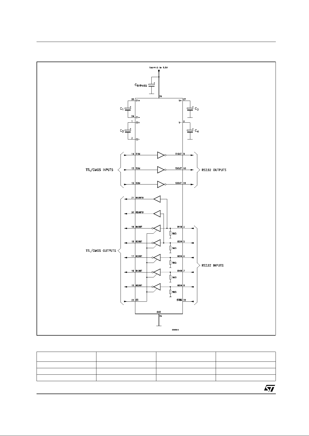
DIM.
mm. inch
MIN. TYP MAX. MIN. TYP. MAX.
A 2.65 0.104
a1 0.1 0.3 0.004 0.012
b 0.35 0.49 0.014 0.019
b1 0.23 0.32 0.009 0.012
C 0.5 0.020
c1 45˚ (typ.)
D 17. 70 18.10 0.697 0.713
E 10.00 10.65 0.393 0.419
e 1.27 0.050
e3 16.51 0.650
F 7.40 7.60 0. 291 0.300
L 0.50 1.27 0.020 0.050
S ˚ (max.)
SO-28 MECHANICAL DATA
0016023
8

ST3241E
8/10
DIM.
mm. inch
MIN. TYP MAX. MIN. TYP. MAX.
A 2 0.079
A1 0.050 0.002
A2 1.65 1.75 1.85 0.065 0.069 0.073
b 0.22 0.38 0.009 0.015
c 0.09 0.25 0.004 0.010
D 9.9 10.2 10.5 0.390 0.402 0.413
E 7.4 7.8 8.2 0.291 0.307 0.323
E1 5 5.3 5.6 0.197 0.209 0.220
e 0.65 BSC 0.0256 BSC
K 0˚ 10˚ 0˚ 10˚
L 0.55 0.75 0.95 0.022 0.030 0.037
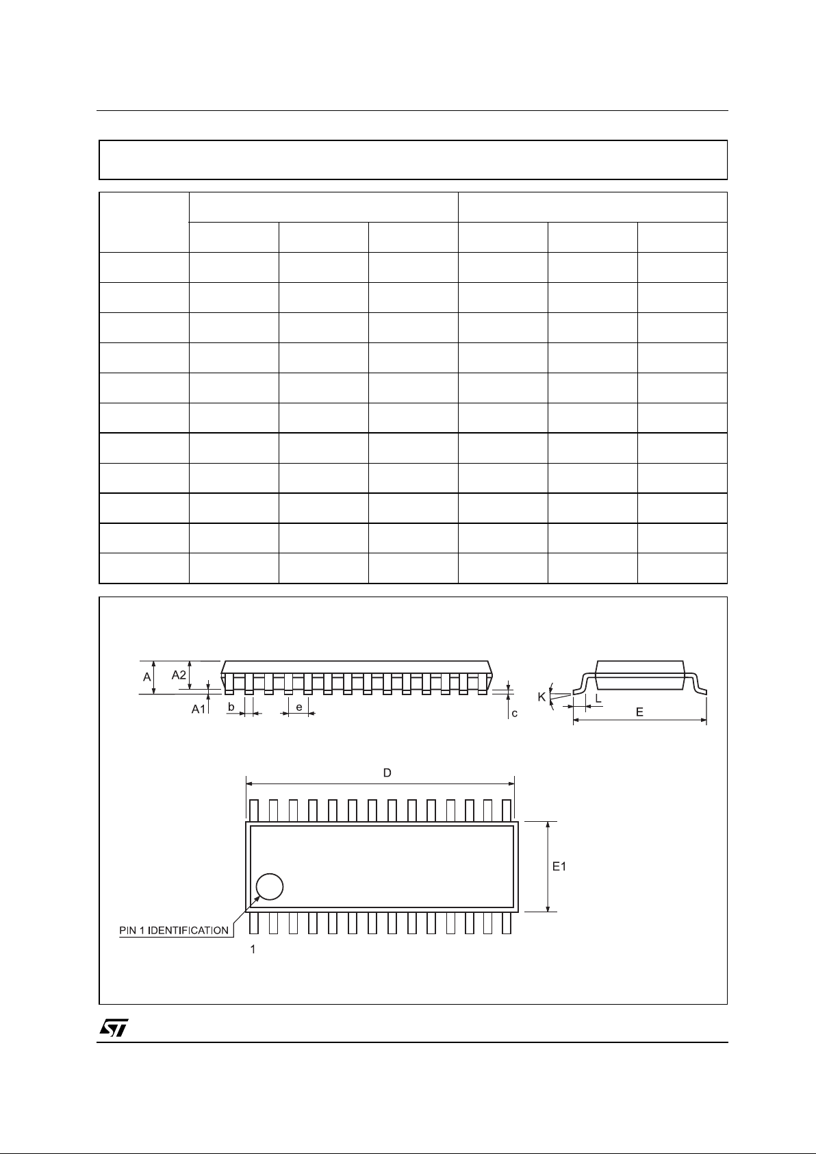
SSOP28 MECHANICAL DATA
ST3241E
9/10
DIM.
mm. inch
MIN. TYP MAX. MIN. TYP. MAX.
A 1.2 0.047
A1 0.05 0.15 0.002 0.004 0.006
A2 0.8 1 1.05 0.031 0.039 0.041
b 0.19 0.30 0.007 0.012
c 0.09 0.20 0.004 0.0089
D 9.6 9.7 9.8 0.378 0.382 0.386
E 6.2 6.4 6.6 0.244 0.252 0.260
E1 4.3 4.4 4.48 0.169 0.173 0.176
e 0.65 BSC 0.0256 BSC
K0˚ 8˚0˚ 8˚
L 0.45 0.60 0.75 0.018 0.024 0.030
TSSOP28 MECHANICAL DATA
0128292B

ST3241E
10/10
Information furnished is believed to be accurate and reliable. However, STMicroelectronics assumes no responsibilit y for the
consequences of use of such informatio n nor for any infringement of paten ts or o ther rig hts of t hird part ies which ma y result from
its use. No license is granted by implication or otherwise under any patent or patent rights of STMicroelectronics. Specifications
mentioned in this publication are subject to change without notice. This publication supersedes and replaces all information
previousl y suppl ied. STM icroel ectronics produc ts are not auth orized for use as c ritica l compone nts in l ife s upport dev ices or
systems without express written approval of STMicroelectronics.
© The ST logo is a registered trademark of STMicroelectronics
© 2002 STMicroelectronics - Printed in Italy - All Rights Reserved
STMicroelectronics GROUP OF COMPANIES
Australia - Brazil - Canada - China - Finland - France - Germany - Hong Kong - India - Israel - Italy - Japan - Malaysia - Malta - Morocco
Singapore - Spain - Sweden - Switzerland - United Kingdom - United States.
© http://www.st.com
 Loading...