

SGS Thomson Microelectronics ST3237ECTR, ST3237ECPR, ST3237ECD, ST3237EBTR, ST3237EBPR Datasheet
...
±15KV ESD-PROTECTED, 1µA, 3 TO 5.5V, 250KBPS,
RS-232 TRANSCEIVER WITH STAND-BY
■ EDS PROTECTION FOR RS-232 I/O PINS:
±15KV HUMAN BODY MODEL
±8KV IEC 1000-4-2 CONTACT DISCHARGE
■ 1µA LOW POWER SHUTDOWN WITH
RECEIVERS ACTIVE
■ GUARENTEED DATA RATE
250Kbps (Normal Operation)
1Mbps (Very High Speed Operation)
■ GUARANTEED SLEW RATE RANGE
6V/µs (Normal Operation)
24V/µs (Very High Speed Operat ion)
■ 0.1µF EXTERNAL CAPACITORS
■ FLOW-THROUGH PINOUT
■ AVAILABLE IN SO-28, SSOP-28 AND
TSSOP28
■ LOW SUPPLY CURRENT 300µA
DESCRIPTION
The ST3237E is a 3V to 5.5V powered EIA/
TIA-232 and V.28/V.24 communication interfaces
high data-rate capability and enhanced
electrostatic discharge (ESD) protection at ±8KV
using IEC1000-4-2 contact discharge and ±15kV
using H uman Body Model (HBM). The other p ins
are protected with standard ESD protection at
±2kV using HBM method. The ST3237C is a
transceiver (5 drive rs, 3 receivers) for fast modem
applications.
The device has a proprietary low-dropout
transmitter output stage prov iding true RS-232
ST3237E
SOP
SSOP
performance from a 3V to 5.5V supply using a
dual charge pump. The device is guaranteed to
run at data rates of 250Kbps in the normal
operation m ode and 1Mbps in the very high speed
operation mode while maintaining RS-232 output
levels.
TSSOP
ORDERING CODES
Type
ST3237ECD 0 to 70 °C SO-28 (Tube) 27parts per tube / 12tube per box
ST3237EBD -40 to 85 °C SO-28 (Tube) 27parts per tube / 12tube per box
ST3237ECDR 0 to 70 °C SO-28 (Tape & Reel) 1000 parts per reel
ST3237EBDR -40 to 85 °C SO-28 (Tape & Reel) 1000 parts per reel
ST3237ECPR 0 to 70 °C SSOP-28 (Tape & Reel) 1350 parts per reel
ST3237EBPR -40 to 85 °C SSOP-28 (Tape & Reel) 1350 parts per reel
ST3237ECTR (*) 0 to 70 °C TSSOP28 (Tape & Reel) 2500 parts per reel
ST3237EBTR -40 to 85 °C TSSOP28 (Tape & Reel) 2500 parts per reel
Temperature
Range
Package Comments
1/13January 2003
ST3237E
PIN DESCRIPTION
PlN N° SYMBOL NAME AND FUNCTION
1
2 GND Ground
3
4 V- -5.5V Generated by the Charge Pump
5
6
7
8
9
10
11
12
13 EN
14 SHDN
15 VHSCI Very High Speed Control Input. Connected to GND for normal
16
17
18
19
20
21
22
23
24
25
26
27 V+ 5.5V Generated by the Charge Pump
28
C
+ Positive Terminal of Inverting Charge Pump Capacitor
2
- Negative Terminal of Inverting Charge Pump Capacitor
C
2
T1
T2
T3
T4
T5
R1
R2
R3
OUT
OUT
OUT
IN
IN
OUT
IN
OUT
First Transmitter Output Voltage
Second Transmitter Output Voltage
Third Transmitter Output Voltage
First Receiver Input Voltage
Second Receiver Input Voltage
Fourth Transmitter Output Voltage
Third Receiver Input Voltage
Fifth Transmitter Output Voltage
Receiver Enable, Active Low
Shutdown Control, Active Low
operation; connected to VCC for 1Mbps transmission rates.
R1
OUTB
T5
IN
R3
OUT
T4
IN
R2
OUT
R1
OUT
T3
IN
T2
IN
T1
N
- Negative Terminal of Voltage-Doubler Charge Pump Capacitor
C
1
V
CC
+ Positive Terminal of Voltage-Doubler Charge Pump Capacitor
C
1
Non Inverting Complementary Receiver Output. Always Active.
Fifth Transmitter Input Voltage
Third Receiver Output Voltage
Fourth Transmitter Input Voltage
Second Receiver Output Voltage
First Receiver Output Voltage
Third Transmitter Input Voltage
Second Transmitter Input Voltage
First Transmitter Input Voltage
Supply Voltage
2/13
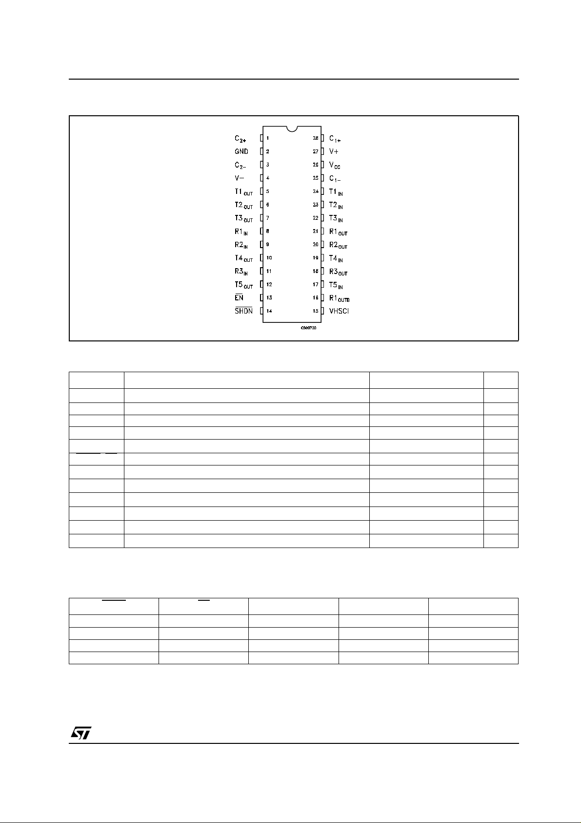
PIN CONFIGURATION
ST3237E
ABSOLUTE MAXIMUM RATINGS
Symbol Parameter Value Unit
V
CC
Supply Voltage
-0.3 to 6 V
V+ Doubled Voltage Terminal -0.3 to 7 V
V- Inverted Voltage Terminal 0.3 to -7 V
V+ +|V-| 13 V
T
IN
SHDN
VHSCI
R
IN
T
OUT
R
OUT,ROUTB
t
SHORT
T
stg
Absolute Maximum Ratings are those values beyond which damage to the device may occur. Functional operation under these condition is
not implied. V+ and V- can have a maximum magnitude of +7V, but their absolute addition can not exceed 13 V.
Transmitter Input Voltage Range
-0.3 to 6 V
,EN -0.3 to 6 V
Very High Speed Control Input -0.3 to (V
Receiver Input Voltage Range
Transmitter Output Voltage Range
+0.3)
CC
± 25 V
± 13.2 V
Receiver Output Voltage Range -0.3 to (VCC+ 0.3)
Short Circuit Duration on T
Storage Temperature Range
(one at a time)
OUT
Continuous
-65 to 150 °C
V
V
SHUTDOWN AND ENABLE CONTROL TRUTH TABLE
SHDN
0 0 High Z Active Active
0 1 High Z High Z Active
1 0 Active Active Active
1 1 Active High Z Active
EN T-OUT R-OUT R-OUTB
3/13
ST3237E
ESD PERFORMANCE: T RANSMITTER OUTPUTS, RECEIVER INPUTS
Symbol Parameter Test Conditions Min. Typ. Max. Unit
ESD ESD Protection Voltage Human Body Model ±15 kV
ESD ESD Protection Voltage IEC-1000-4-2 Contact Discharge ±8kV
ELECTRICAL CHARACTERISTICS
(C
Typical values are referred to T
Symbol Parameter Test Conditions Min. Typ. Max. Unit
I
SUPPLYVCC
I
LOGIC INPUT ELECTRICAL CHARACTERISTICS
(C
Typical values are referred to T
Symbol Parameter Test Conditions Min. Typ. Max. Unit
Note 1: Transmitter input hysteresis is typically 250mV
=0.1µF, VCC=3Vto5.5V,TA= -40 to 85°C, unles s otherwise specified.
1-C4
=25°C)
A
Power Supply Current SHDN=V
SHDN
1-C4
V
V
Shutdown Supply Current SHDN=GND V
=0.1µF, VCC=3Vto5.5V,TA= -40 to 85°C, unles s otherwise specified.
=25°C)
A
Input Logic Threshold Low
V
TIL
(Note 1)
Input Logic Threshold High T-IN, VHSCI, EN,SHDN VCC= 3.3V 2 V
TIH
Input Leakage Current T-IN, VHSCI, EN,SHDN ± 1.0 µA
I
IL
Transmitter Input
HYS
Hysteresis
T-IN, VHSCI, EN,SHDN 0.8 V
CC
No Load 0.3 1 mA
=GND or V
T_IN
CC
=5V 2.4
V
CC
15µA
0.25 V
TRANSMITTER EL ECTRICAL CHARACTERISTICS
(C
Typical values are referred to T
Symbol Parameter Test Conditions Min. Typ. Max. Unit
V
R
=0.1µF tested at 3.3V±10%, VCC=3Vto5.5V,TA= -4 0 to 85°C, unless otherwise specified.
1-C4
TOUT
TOUT
I
SC
I
TOL
Output Voltage Swing All Transmitter outputs are loaded with
Transmitter Output
Resistance
Output Short Circuit Current ± 60 mA
Output Leakage Current VCC= 0V or 3.3V to 5.5V V
=25°C)
A
3KΩ to GND
VCC=0V V
± 5 ± 5.4 V
= ± 2V 300 10M Ω
OUT
= ± 12V
OUT
Transmitters Disable
± 25 µA
4/13
 Loading...