

SGS Thomson Microelectronics ST3222CTR, ST3222CDR, ST3222CD, ST3222BDR, ST3222BD Datasheet
3 TO 3.6V, LOW PO WER, UP TO 400KBPS,
RS-232 DRIVERS AND RECEIVERS
■ 300µA SUPPLY CURRENT
■ 250Kbps MINIMUM GUARENTEED DATA
RATE
■ 6V/µs MINIMUM GUARANTEED SLEW RATE
■ MEET EIA/TIA-232SPECIFICATIONSDOWN
TO 3V
■ AVAILABLEINSO-18ANDTSSOP20
ST3222
DESCRIPTION
SOP TSSOP
The ST3222 is a 3V powered EIA/TIA-232 and
V.28/V.24 communications interface with low
power requirements and high data-rate
capabilities. ST3222 has a proprietary low dropout
transmitter output stage providing true RS-232
performance from 3 to 3.6V power supplies. The
device requires only four small 0.1µF standard
external capacitors for operating from 3V s upply.
The ST3222 has t w o r ec eivers and two drivers.
TheST3222featuresa1µA shutdown mode that
reduces power consumption and extends battery
life in portable systems. Its receivers can remain
active in shutdown mode, allowing external
devices s uc h as modems to be moni tored using
only1µAsupply current.
The device is guaranteed to run at da ta rates of
250Kbps while maintaining RS-232 output levels.
Typical applications are Notebook, Subnotebook
and Palmtop Computers, Battery Powered
Equipment, Hand-Held Equipment, Peripherals
and Printers.
ORDERING CODES
Type
ST3222CD 0 to 70 °C SO-18 (Tube) 50parts per tube / 20tube per box
ST3222BD -40 to 85 °C SO-18 (Tube) 50parts per tube / 20tube per box
ST3222CDR 0 to 70 °C SO-18 (Tape & Reel) 1000 parts per reel
ST3222BDR -40 to 85 °C SO-18 (Tape & Reel) 1000 parts per reel
ST3222CTR 0 to 70 °C TSSOP20 (Tape & Reel) 2500 parts per reel
ST3222BTR -40 to 85 °C TSSOP20 (Tape & Reel) 2500 parts per reel
Temperature
Range
Package Comments
1/9October 2002
ST3222
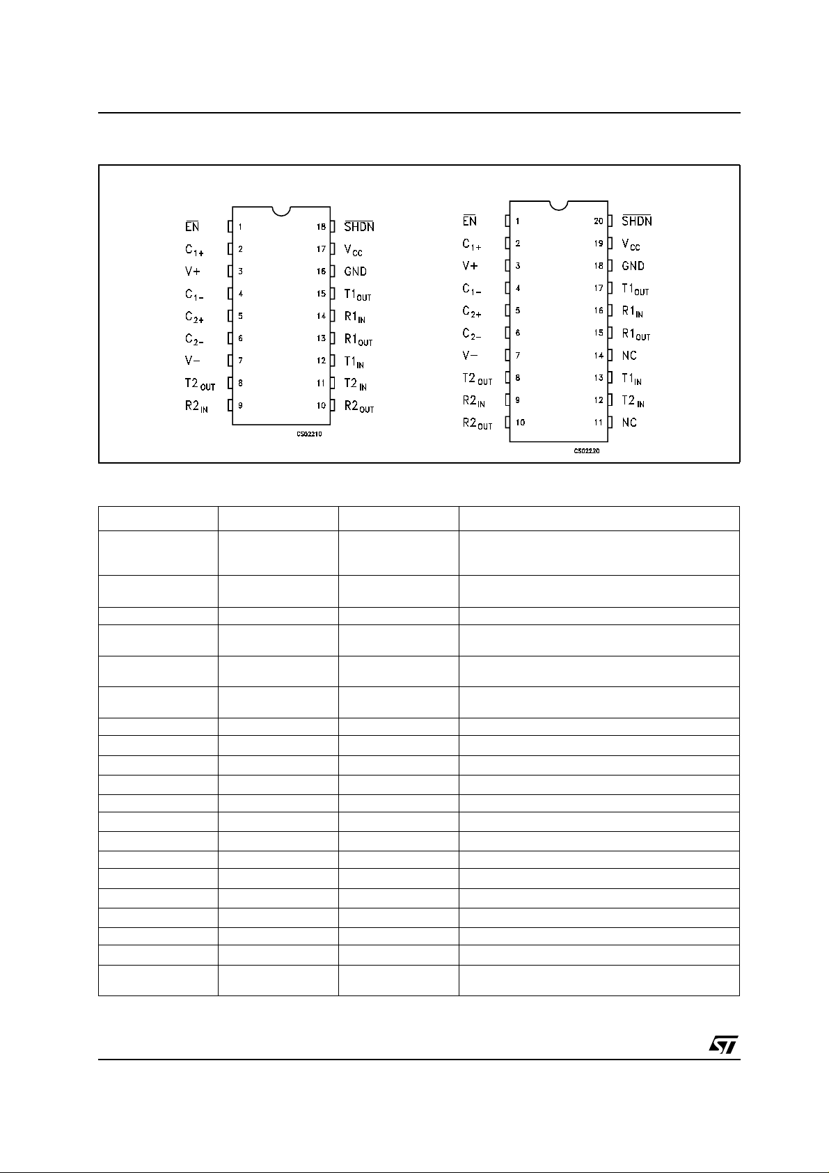
PIN CONFIGURATION
PIN DESCRIPTION
SO-18 TSSOP20
PlN N° (SO-18) PlN N° (TSSP20) SYMBOL NAME AND FUNCTION
1 1 EN Receiver Enable Control. Drive low for normal
operation. Drive high to force the receivers outputs
(R_OUT) into a high-impedance state.
22
+
C
1
Positive Terminal for the first Charge Pump
Capacitor
3 3 V+ 5.5V Generated By The Charge Pump.
44
55
66
-
C
1
+
C
2
-
C
2
Negative Terminal for the first Charge Pump
Capacitor
Positive Terminal for the second Charge Pump
Capacitor
Negative Terminal for the second Charge Pump
Capacitor
7 7 V- -5.5V Generated By The Charge Pump.
88
99
10 10
T2
R2
R2
OUT
IN
OUT
Second Transmitter Output Voltage
Second Receiver Input Voltage
Second Receiver Output Voltage
11 NC Not Connected
11 12
12 13
T2
T1
IN
IN
Second Transmitter Input Voltage
First Transmitter Input Voltage
14 NC Not Connected
13 15
14 16
15 17
R1
T1
R1
OUT
IN
OUT
First Receiver Output Voltage
First Receiver Input Voltage
First Transmitter Output Voltage
16 18 GND Ground
17 19
V
CC
Supply Voltage
18 20 SHDN Active Low Shutdown Control Input. Drive Low To
Shut-down Trnasmittes And Charge Pump
2/9

ST3222
ABSOLUTE MAXIMUM RATINGS
Symbol Parameter Value Unit
V
V+
V- Inverted Voltage Terminal 0.3 to -7 V
V+ +|V-| 13 V
T
SHDN
R
T
OUT
R
OUT
t
SHORT
Absolute Maximum Ratings are those values beyond which damage to the device may occur. Functional operation under these condition is
not implied. V+ and V- can have a maximum magnitude of +7V, but their absolute addition can not exceed 13 V.
ELECTRICAL CHARACTERISTICS
(C
1-C4
Typical values are referred to T
Symbol Parameter Test Conditions Min. Typ. Max. Unit
I
SUPPLYVCC
I
SHDN
Supply Voltage
CC
Doubled Voltage Terminal (V
Transmitter Input Voltage Range
IN
-0.3 to 6 V
-0.3)to7
CC
-0.3 to 6 V
Transmitter Input Voltage Range -0.3 to 6 V
Receiver Input Voltage Range
IN
Transmitter Output Voltage Range
± 25 V
± 13.2 V
Receiver Output Voltage Range -0.3 to (VCC+ 0.3)
Transmitter Output Short to GND Time
Continuous
=0.1µF, VCC=3Vto3.6V,TA= -40 to 85°C, unles s otherwise specified.
=25°C)
A
Power Supply Current No Load VCC= 3.3V TA=25°C
=V
SHUTDOWN Supply
Current
SHDN
No Load VCC= 3.3V TA=25°C
SHDN
=V
CC
CC
0.3 1 mA
110µA
V
V
LOGIC INPUT ELECTRICAL CHARACTERISTICS
(C
Typical values are referred to T
Symbol Parameter Test Conditions Min. Typ. Max. Unit
Note 1: Transmitter input hysteresis is typically 250mV
=0.1µF, VCC=3Vto3.6V,TA= -40 to 85°C, unles s otherwise specified.
1-C4
=25°C)
A
V
Input Logic Threshold Low T-IN, EN, SHDN (Note 1) 0.8 V
IL
Input Logic Threshold High VCC= 3.3V 2 V
V
IH
V
Transmitter Input
HYS
Histeresys
I
Input Leakage Current T-IN, EN, SHDN ± 0.01 ± 1 µA
IL
0.5 V
TRANSMITTER EL ECTRICAL CHARACTERISTICS
(C
Typical values are referred to T
Symbol Parameter Test Conditions Min. Typ. Max. Unit
V
R
=0.1µFVCC=3Vto3.6V,TA= -40 to 85°C, u nless otherwi se specified.
1-C4
TOUT
TOUT
I
TSC
I
TOL
Output Voltage Swing All Transmitter outputs are loaded with
Transmitter Output
Resistance
Output Short Circuit Current ± 60 mA
Output Leakage Current VCC= 0V or 3V to 3.6V V
=25°C)
A
3KΩ to GND
VCC=V+=V-=0V V
= ± 2V 300 10M Ω
OUT
= ± 12V
OUT
Transmitters Disable
± 5 ± 5.4 V
± 25 µA
3/9
 Loading...