

■ TTLINPUT COMPATIBLE
■
TYPICAL PROPAGATIONDELAY:6ns
■ TYPICALOUTPUTSKEW:0.5ns
■ OUTPUTWILLNOTLOADLINEWHEN
=0V
V
CC
■ MEETSTHEREQUIREMENTSOFEIA
STANDARDRS-422
■ OPERATIONFROMSINGLE5VSUPPLY
■ 3-STATEOUTPUTS FORCONNECTIONTO
SYSTEMBUSES
■ LOWQUIESCENTCURRENT
■
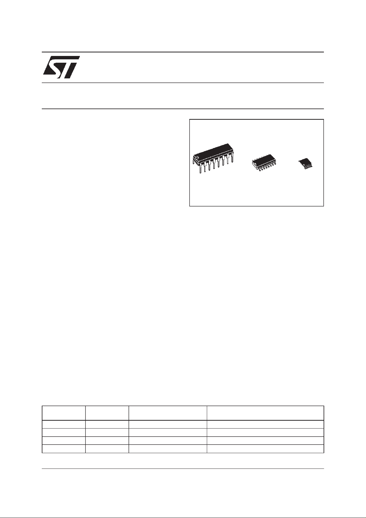
AVAILABLEIN SURFAC EMOU N T
DESCRIPTION
The ST26C31 is a quad differential line driver
designed for digital data trasmission over
balanced lines and meets all the requirements of
EIA standard RS-422 while retaining the low
powercharacteristicsof CMOS.
The ST26C31 accepts TTL or CMOS input levels
ST26C31
CMOS QUAD TRI-STATE
DIFFERENTIALLINE DRIVER
SOPDIP TSSOP
and translates these to RS-422 output levels.
This part uses special outputs circuitry common
to all four drivers. All outputs are protected
against damage due to electrostatic discharge by
diodeto V
and ground.
CC
ORDERCODES
Typ e Temp erature
Range
ST26C31BN -40 to 85
ST26C31BD -40 to 85
ST26C31BDR -40 to 85
ST26C31BTR -40 to 85
April 2000
Packag e Commen ts
o
C DIP-16 25 parts per tube / 40 tube per box
o
C SO-16 (Tube) 50 parts per tube / 20 tube per box
o
C SO-16 (Tape & Reel) 2500 parts per reel
o
C TSSOP16 (Tape & Reel) 2500 parts per reel
1/8
ST26C31
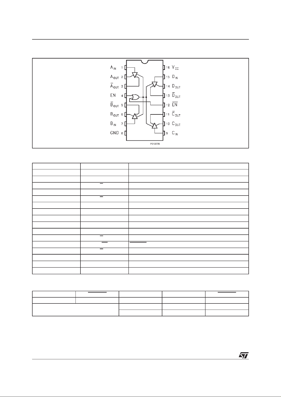
PIN CONFIGURATION
PIN DESCRIPTION
PIN No SYMBOL NAM E AND FUNCTI O N
1A
2A
3A
4 EN ENABLE
5B
6B
7B
8 GND Ground
9C
10 C
11 C
12 EN ENABLE
13 D
14 D
15 D
16 V
IN
OUT
OUT
OUT
OUT
IN
IN
OUT
OUT
OUT
OUT
IN
CC
INPUT A
Channel A Output
Channel A Output
Channel B Output
Channel B Output
INPUT B
INPUT C
Channel C Output
Channel C Output
Channel D Output
Channel D Output
INPUT D
Supply Voltage
TRUTH TABLE
ENABLE ENABLE INPUT OUT PUT OUTPUT
LHXZZ
All other combinations of enable inputs L L H
HHL
L=Low VoltageState
H=HighLogicState
X=Don’t Care
Z=High Impedance
2/8

ST26C31
ABSOLUTE MAXIMUM RATINGS
(Note 1, 2)
Symb o l Para met er Val u e Unit
V
V
V
OUT
I
I
OUT
I
CC
T
Note1: AbsoluteMaximum Ratingsarethose values beyond which thesafety of thedevice cannot beguaranteed. They are not meant to imply thatthe
deviceshould be operated atthese limits.The table of electricalcharacteristics provide conditionsforactual device operation.
Note2:Unlessotherwisespecified,allvoltagearereferenced toground.Allcurrentsintothedevicepinsarepositive; allcurrents outofthedevicepinsare
negative.
Supply Voltage -0.5 to 7 V
CC
DC Input Voltage - 0.5 to (VCC+ 0.5) V
IN
DC Output Voltage (High or Low State) -0.5 to 7.0 V
Clamp Diode Current
IK
20 mA
±
DC Output Current per Pin ± 150 mA
DC VCCor GND Current
Storage Temperature Range -65 to +150
stg
150 mA
±
o
C
RECOMMENDEDOPERATINGCONDITIONS
Symbol Parameter Value Unit
Supply Voltage 4.5 to 5.5 V
CC
DC Input Voltage 0 to V
IN
DC Output Voltage (High or Low State) 0 to V
CC
CC
DC Output Voltage (VCC=0V or High Impedance) 0 to 5 V
Operating Temperature Range -40 to +85
A
Maximum Enable Input Rise or Fall Times 500 ns
V
V
o
C
V
V
V
V
t
OUT
OUT
T
r,tf
3/8

ST26C31
ELECTRICALCHARACTERISTICS
=5V±10% unlessotherwisespecified, Note 1)
(V
CC
Symbol Parameter Test Conditio ns Value Un it
Min. Typ. Max.
High Level Input Voltage 2 V
V
IH
Low Level Input Voltage 0.8 V
V
IL
V
V
V
High Level Output Voltage VIN=VIHor VIL,I
OH
Low Level Output Voltage VIN=VIHor VIL,I
OL
Differential Output Voltage RL=100Ω(Note 2) 2 3.1 V
V
T
Difference in Differential
T-VT
RL=100Ω(Note 2) 0.4 V
= -20mA 2.5 3.4 V
OUT
= +20mA 0.3 0.5 V
OUT
Output Voltage
Common Mode Output
V
OS
RL=100Ω(Note 2) 1.8 3 V
Voltage
|V
-
Difference in Common Mode
OS
V
|
Output Voltage
OS
Input Current VIN=VCC, GND, VIHor V
I
IN
Quiescent Supply Current
I
CC
(Note 2)
=100Ω(Note 2) 0.4 V
R
L
IL
I
=0µAVIN=VCCor GND 200 500
OUT
= 2.4 or 0.5V
V
IN
0.8 2 mA
±1.0 µA
µ
(Note 3)
3-STATE Output Leakage
I
OZ
Current
Output Short Circuit Current VIN=VCCor GND
I
SC
V
OUT=VCC
ENABLE = V
or GND
IL
ENABLE= V
0.5
±
IH
-30 -150 mA
5.0
±
µ
(Notes 2, 4)
Power Off Output Leakage
I
OFF
Current (Note 2)
Note1:Unlessotherwisespecified,min/maxlimitsapplyacross therecommended operatingtemperature range. AlltypicalsaregivenforVCC=5V and
T
=25oC
a
Note2:SeeEIASpecificationRS422forexact testconditions.
Note3:Measuredperpininput.Allotherinput atV
Note4: This isthe current sourced when ahigh output isshorted toground. Only oneoutput at time should be shorted.
VCC=0V V
orGND
CC
= 6 V 100 µA
OUT
= -0.25 V -100
V
OUT
µ
A
A
A
SWITCHING CHARACTERISTICS(VCC=5V±10%, tr=tf≤6ns, See Note 1)
Symbol Parameter Test Conditio ns Value Un it
Min. Typ. Max.
Propagation Delay Input to
t
PLH
Output
t
PHL
Skew (Note 2) S1 Open 0.5 2 ns
Differential Output Rise and
t
TLH
Fall Times
t
THL
Output Enable Time S1 Closed 11 19 ns
t
PZH
Output Enable Time S1 Closed 13 21 ns
t
PZL
Output Disable Time (Note 3) S1 Closed 5 9 ns
t
PHZ
Output Disable Time (Note 3) S1 Closed 7 11 ns
t
PLZ
Power Dissipation
C
PD
Capacitance (Note 4)
Input Capacitance 6 pF
C
IN
Note1:Unlessotherwisespecified.min/maxlimitsapplyacross therecommended operatingtemperature range. AlltypicalaregivenforVCC= 5V and
=25oC
T
a
Note2: Skewis defined as the differenceinpropagation delays be tween complementary outputs atthe 50% point.
Note3:Outputdisabletimeisthedelayfromthecontrolinputbeingswitched totheoutputtransistorsturningoff.Theactualdisabletimesarelessthan
indicatedduetothedelayaddedbyRCtimeconstantoftheload.
Note4:C
P
D=CPDVCC
determinestheno loaddynamicpowerconsumption, PD=CPDV
PD
f+I
CC
4/8
S1 Open 2 6 11 ns
S1 Open 6 10 ns
50 pF
2
f+ICCVCC, and theno loaddynamic currentconsumption,
CC

Plastic DIP-16 (0.25) MECHANICAL DATA
ST26C31
DIM.
MIN. TYP. MAX. MIN. TYP. MAX.
a1 0.51 0.020
B 0.77 1.65 0.030 0.065
b 0.5 0.020
b1 0.25 0.010
D 20 0.787
E 8.5 0.335
e 2.54 0.100
e3 17.78 0.700
F 7.1 0.280
I 5.1 0.201
L 3.3 0.130
Z 1.27 0.050
mm inch
P001C
5/8

ST26C31
SO-16 MECHANICAL DATA
DIM.
MIN. TYP. MAX. MIN. TYP. MAX.
A 1.75 0.068
a1 0.1 0.2 0.004 0.007
a2 1.65 0.064
b 0.35 0.46 0.013 0.018
b1 0.19 0.25 0.007 0.010
C 0.5 0.019
c1 45 (typ.)
D 9.8 10 0.385 0.393
E 5.8 6.2 0.228 0.244
e 1.27 0.050
e3 8.89 0.350
F 3.8 4.0 0.149 0.157
G 4.6 5.3 0.181 0.208
L 0.5 1.27 0.019 0.050
M 0.62 0.024
S 8 (max.)
mm inch
6/8
P013H

TSSOP16 MECHANICAL DATA
ST26C31
DIM.
mm inch
MIN. TYP. MAX. MIN. TYP. MAX.
A 1.1 0.433
A1 0.05 0.10 0.15 0.002 0.004 0.006
A2 0.85 0.9 0.95 0.335 0.354 0.374
b 0.19 0.30 0.0075 0.0118
c 0.09 0.20 0.0035 0.0079
D 4.9 5 5.1 0.193 0.197 0.201
E 6.25 6.4 6.5 0.246 0.252 0.256
E1 4.3 4.4 4.48 0.169 0.173 0.176
e 0.65 BSC 0.0256 BSC
K0
o
o
4
o
8
o
0
o
4
8
L 0.50 0.60 0.70 0.020 0.024 0.028
o
A2
A
A1
PIN 1 IDENTIFICATION
b
e
c
K
L
E
D
E1
1
7/8

ST26C31
Information furnished isbelieved to be accurate and reliable. However,STMicroelectronics assumes no responsibility for the consequences
of use of such information nor for any infringement of patents or other rights of third parties which may result from its use. No license is
granted by implication or otherwise under any patent or patent rights of STMicroelectronics. Specification mentioned in thispublication are
subject tochange without notice. Thispublication supersedes and replaces all information previously supplied. STMicroelectronics products
are not authorized for use as criticalcomponents in lifesupport devices or systems withoutexpress written approval of STMicroelectronics.
The ST logo isa registeredtrademark of STMicroelectronics
2000 STMicroelectronics – Printed in Italy – All RightsReserved
STMicroelectronics GROUP OF COMPANIES
Australia - Brazil- China - Finland - France - Germany - Hong Kong - India - Italy - Japan- Malaysia - Malta - Morocco
Singapore - Spain- Sweden - Switzerland - United Kingdom - U.S.A.
http://www.st.com
.
8/8
 Loading...