SGS Thomson Microelectronics ST26C31BTR, ST26C31BN, ST26C31BDR, ST26C31BD Datasheet

■ TTLINPUT COMPATIBLE
■
TYPICAL PROPAGATIONDELAY:6ns
■ TYPICALOUTPUTSKEW:0.5ns
■ OUTPUTWILLNOTLOADLINEWHEN
=0V
V
CC
■ MEETSTHEREQUIREMENTSOFEIA
STANDARDRS-422
■ OPERATIONFROMSINGLE5VSUPPLY
■ 3-STATEOUTPUTS FORCONNECTIONTO
SYSTEMBUSES
■ LOWQUIESCENTCURRENT
■
AVAILABLEIN SURFAC EMOU N T
DESCRIPTION
The ST26C31 is a quad differential line driver
designed for digital data trasmission over
balanced lines and meets all the requirements of
EIA standard RS-422 while retaining the low
powercharacteristicsof CMOS.
The ST26C31 accepts TTL or CMOS input levels
ST26C31
CMOS QUAD TRI-STATE
DIFFERENTIALLINE DRIVER
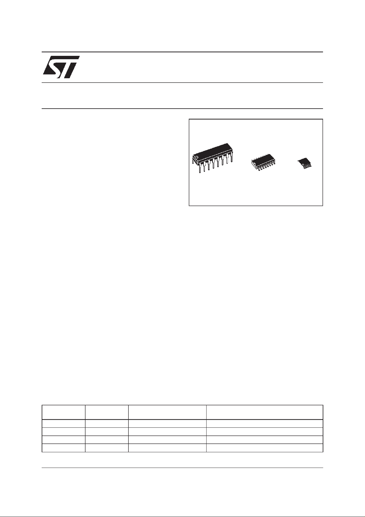
SOPDIP TSSOP
and translates these to RS-422 output levels.
This part uses special outputs circuitry common
to all four drivers. All outputs are protected
against damage due to electrostatic discharge by
diodeto V
and ground.
CC
ORDERCODES
Typ e Temp erature
Range
ST26C31BN -40 to 85
ST26C31BD -40 to 85
ST26C31BDR -40 to 85
ST26C31BTR -40 to 85
April 2000
Packag e Commen ts
o
C DIP-16 25 parts per tube / 40 tube per box
o
C SO-16 (Tube) 50 parts per tube / 20 tube per box
o
C SO-16 (Tape & Reel) 2500 parts per reel
o
C TSSOP16 (Tape & Reel) 2500 parts per reel
1/8

ST26C31
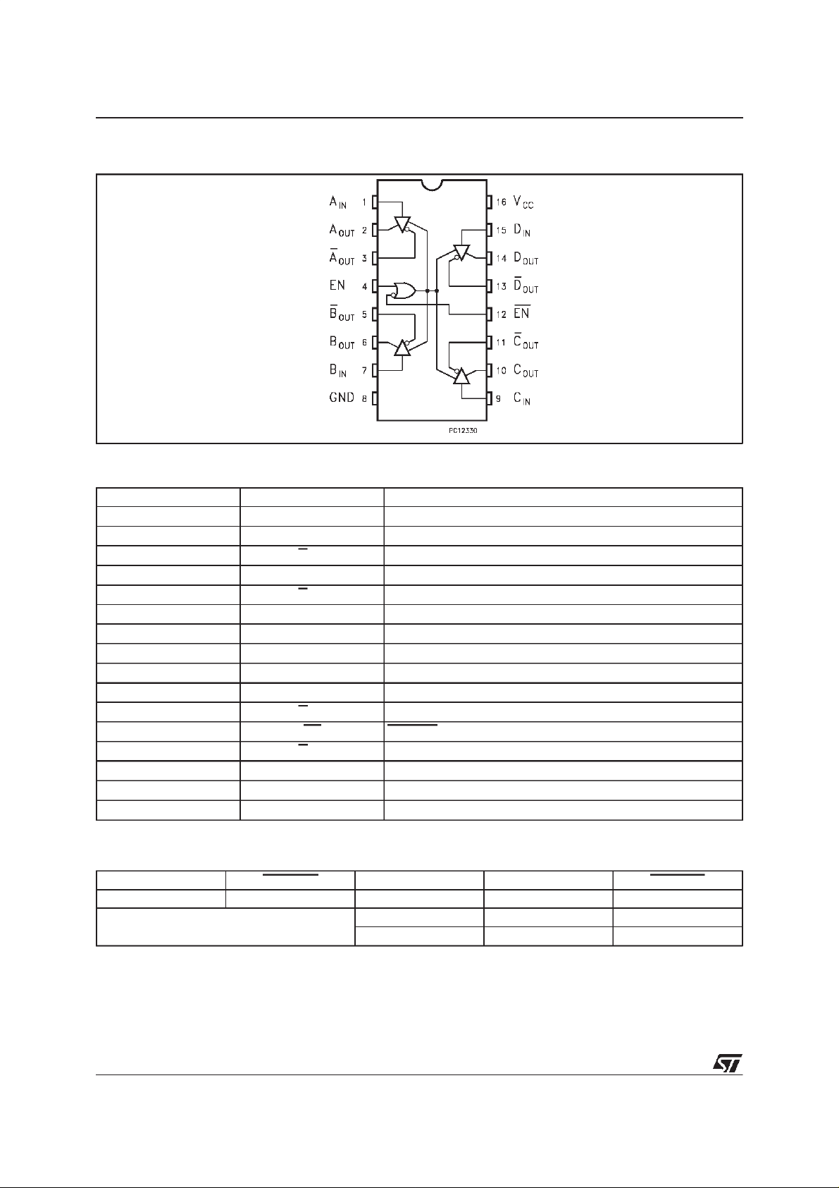
PIN CONFIGURATION
PIN DESCRIPTION
PIN No SYMBOL NAM E AND FUNCTI O N
1A
2A
3A
4 EN ENABLE
5B
6B
7B
8 GND Ground
9C
10 C
11 C
12 EN ENABLE
13 D
14 D
15 D
16 V
IN
OUT
OUT
OUT
OUT
IN
IN
OUT
OUT
OUT
OUT
IN
CC
INPUT A
Channel A Output
Channel A Output
Channel B Output
Channel B Output
INPUT B
INPUT C
Channel C Output
Channel C Output
Channel D Output
Channel D Output
INPUT D
Supply Voltage
TRUTH TABLE
ENABLE ENABLE INPUT OUT PUT OUTPUT
LHXZZ
All other combinations of enable inputs L L H
HHL
L=Low VoltageState
H=HighLogicState
X=Don’t Care
Z=High Impedance
2/8

ST26C31
ABSOLUTE MAXIMUM RATINGS
(Note 1, 2)
Symb o l Para met er Val u e Unit
V
V
V
OUT
I
I
OUT
I
CC
T
Note1: AbsoluteMaximum Ratingsarethose values beyond which thesafety of thedevice cannot beguaranteed. They are not meant to imply thatthe
deviceshould be operated atthese limits.The table of electricalcharacteristics provide conditionsforactual device operation.
Note2:Unlessotherwisespecified,allvoltagearereferenced toground.Allcurrentsintothedevicepinsarepositive; allcurrents outofthedevicepinsare
negative.
Supply Voltage -0.5 to 7 V
CC
DC Input Voltage - 0.5 to (VCC+ 0.5) V
IN
DC Output Voltage (High or Low State) -0.5 to 7.0 V
Clamp Diode Current
IK
20 mA
±
DC Output Current per Pin ± 150 mA
DC VCCor GND Current
Storage Temperature Range -65 to +150
stg
150 mA
±
o
C
RECOMMENDEDOPERATINGCONDITIONS
Symbol Parameter Value Unit
Supply Voltage 4.5 to 5.5 V
CC
DC Input Voltage 0 to V
IN
DC Output Voltage (High or Low State) 0 to V
CC
CC
DC Output Voltage (VCC=0V or High Impedance) 0 to 5 V
Operating Temperature Range -40 to +85
A
Maximum Enable Input Rise or Fall Times 500 ns
V
V
o
C
V
V
V
V
t
OUT
OUT
T
r,tf
3/8
 Loading...