

SGS Thomson Microelectronics ST25W04, ST25C04, ST24W04, ST24C04 Datasheet
with User-Defined Block Write Protection
1 MILLION ERASE/WRITE CYCLES with
40 YEARS DAT A RE TENTION
SINGLE SUPPLY VOLTAGE:
– 3V to 5.5V for ST24x04 versions
– 2.5V to 5.5V for ST25x04 versions
HARDWARE WRITE CONT ROL VERSIONS:
ST24W04 and ST25W04
PROGRAMMABLE WRITE PROTECTION
TWO WIRE SERIAL INTERFACE, FULLY I2C
BUS COMPATIBLE
BYTE and MULTIBYTE WRITE (up to 4
BYTES)
PAGE WRITE (up to 8 BYTES)
BYTE, RANDOM and SEQUENTIAL READ
MODES
SELF TIMED PROGRAMMING CYCLE
AUTOMATIC ADDRESS INCREME NTING
ENHANCE D ESD/LATCH UP
PERFORMANCES
ST24C04, ST25C04
ST24W04, ST25W04
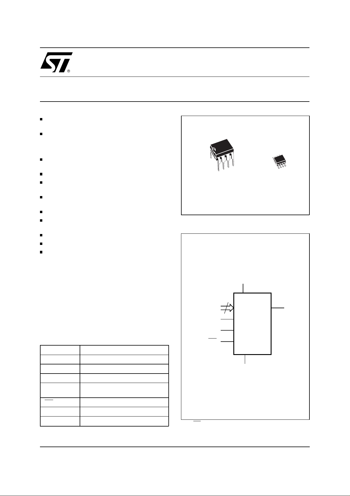
4 Kbit Serial I2C Bus EEPROM
8
1
PSDIP8 (B)
0.25mm Frame
Figure 1. Logic Diagram
8
1
SO8 (M)
150mil Width
V
CC
DESCRIPTION
2
This specification covers a range of 4 Kbits I
EEPROM products, the ST24/25C04 and the
ST24/25W04. In the text, products are referred to
as ST24/25x04, where "x" is: "C" for Standard
version and "W" for hardware Write Control version.
T ab le 1. Signal Names
PRE Write Protect Enable
E1-E2 Chip Enable Inputs
SDA Serial Data Address Input/Output
SCL Serial Clock
MODE
WC Write Control (W version)
V
CC
V
SS
February 1999 1/16
Multibyte/Page Write Mode
(C version)
Supply Voltage
Ground
C bus
2
E1-E2 SDA
PRE
SCL
MODE/WC*
Note:
WC signal is only available for ST24/25W04 products.
ST24x04
ST25x04
V
SS
AI00851E
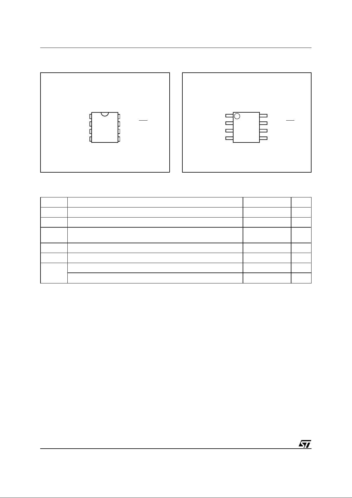
ST24/25C04, ST24/25W04
Figure 2A. DIP Pin Connections
ST24x04
ST25x04
1
PRE V
2
3
E2
4
SS
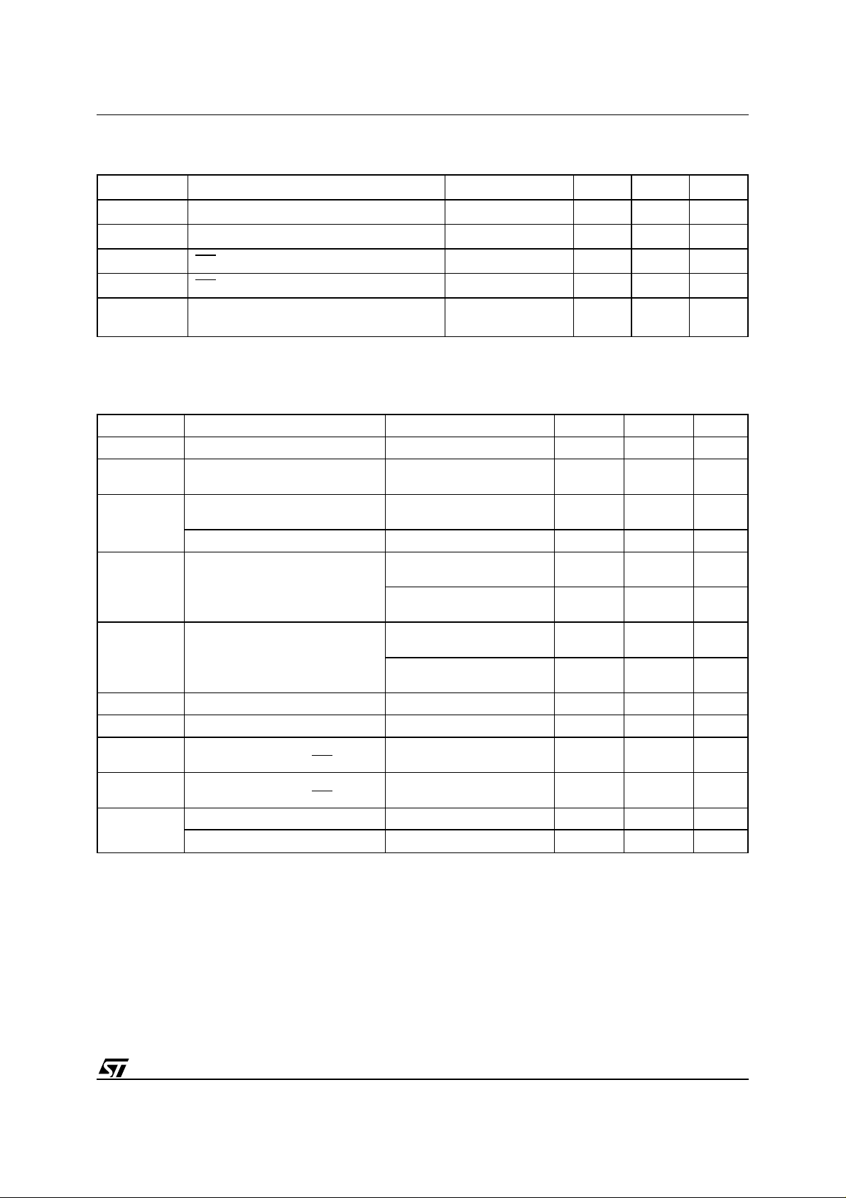
T ab le 2. Absolute Maximum Ratings
Symbol Parameter Value Unit
T
T
V
Notes:
T
STG
LEAD
V
V
ESD
Ambient Operating Temperature –40 to 125
A
Storage Temperature –65 to 150
Lead Temperature, Soldering (SO8 package)
Input or Output Voltages –0.6 to 6.5 V
IO
Supply Voltage –0.3 to 6.5 V
CC
Electrostatic Discharge Voltage (Human Body model)
Electrostatic Discharge Voltage (Machine model)
1. Except for the rating "Operating Temperature Range", stresses above those listed in the Table "Absolute Maximum Ratings"
may cause permanent damage to the device. These are stress rating s only and operation of the device at these or any other
conditions above those indicated in the Operating sections of this specification is not implied. Exposure to Absolute Maximum
Rating conditions for extended periods may affect device reliability. Refer also to the STMicroelectronics SURE Program and other
relevant quality documents.
2. MIL-STD-883C, 3015.7 (100pF, 1500 Ω).
3. EIAJ IC-121 (Condition C) (200pF, 0 Ω).
8
7
6
5
AI00852E
CC
MODE/WCE1
SCL
SDAV
(1)
(PSDIP8 package)
Figure 2B. SO Pin Connections
ST24x04
ST25x04
PRE V
1
2
E2
SS
40 sec
10 sec
(2)
(3)
3
4
8
7
6
5
AI01107E
215
260
4000 V
500 V
CC
MODE/WCE1
SCL
SDAV
C
°
C
°
C
°
DESCRIPTION (cont’d)
The ST24/25x04 are 4 Kbit electrically erasable
programmable memories (EEPROM), organized
as 2 blocks of 256 x8 bits. They are manufactured
in STMicroelectronics’s Hi-Endurance Advanced
CMOS technology which guarantees an endurance of one million erase/write cycles with a data
retention of 40 years.
Both Plastic Dual-in-Line and Plastic Small Out line
packages are available.
2
The memories are compatible with the I
C standard, two wire serial interface which uses a bi-directional data bus and serial clock. The memories
2/16
carry a built-in 4 bit, unique device identification
code (1010) corresponding to the I
2
C bus definition. This is used together with 2 chip enable inputs
(E2, E1) so that up to 4 x 4K devices may be
attached to the I
The memories behave as a slave device in the I
2
C bus and selected individually.
2
protocol with all memory operations synchronized
by the serial clock. Read and write operations ar e
initiated by a START condition generated by the
bus master. The START condition is followed by a
stream of 7 bits (identification code 1010), plus one
read/write bit and terminated by an acknowledge
bit.
C
T ab le 3. Device Select Code
ST24/25C04, ST24/25W04
Device Code Chip Enable
Bit b7 b6 b5 b4 b3 b2 b1 b0
Device Select 1 0 1 0 E2 E1 A8 R
Note:
The MSB b7 is sent first.
T ab le 4. Operating Modes
Mode RW bit MODE Bytes Initial Sequence
Current Address Read ’ 1’ X 1 STAR T, Device Select, R
Random Address Read
Sequential Read ’1’ X 1 to 512 Similar to Current or Random Mode
Byte Write ’0’ X 1 START, Device Select, R
IH
or V
(2)
IL
Multibyte Write
Page Write ’0’ V
Notes:
1. X = V
2. Multibyte Write not available in ST24/25W04 versions.
(1)
’0’
’1’ reSTART, Device Select, R
’0’ V
X1
IH
IL
4 START, Device Select, RW = ’0’
8 START, Device Select, RW = ’0’
START, Device Select, R
Block
Select
W = ’1’
W = ’0’, Address,
W = ’1’
W = ’0’
RW
W
When writing data to the memory it responds to the
8 bits received by asserting an acknowledge bit
during the 9th bit time. When data is read by the
bus master, it acknowledges the receipt of the data
bytes in the same way. Data transfers are terminated with a STOP condition.
Power On Reset: V
lock out write protect . In
CC
order to prevent data corruption and inadvertent
write operations during power up, a Power On
Reset (POR) circuit is implemented. Until the V
CC
voltage has reached the POR threshold value, the
internal reset is active, all operations are disabled
and the device will not respond to any c ommand.
In the same way, when V
drops down from the
CC
operating voltage to below the POR threshold
value, all operations are disabled and the device
will not respond to any command. A stable V
CC
must be applied before applying any logic signal.
SIGNAL DESCRIPTIONS
Serial Clock (SCL). The SCL input pin is used to
synchronize all data in and out of the memory. A
resistor can be connected from the SCL line to V
CC
to act as a pull up (see Figure 3).
Serial Data (SDA). The SDA pin is bi-directional
and is used to transfer data in or out of the memory.
It is an open drain output that may be wire-OR’ed
with other open drain or open collector signals on
the bus. A resistor must be connected from the SDA
bus line to V
to act as pull up (see Figure 3).
CC
Chip Enable (E1 - E2). These chip enable inputs
are used to set the 2 least significant bits (b2, b3)
of the 7 bit device select code. These inputs may
be driven dynamically or tied to V
or VSS to
CC
establish the device select code.
Protect Enable (PRE). The PRE input pin, in ad-
dition to the status of the Block Address Pointer bit
(b2, location 1FFh as in Figure 7), sets the PRE
write protection active.
Mode (M ODE). The MO DE input is available on pin
7 (see also
cally. It must be at V
mode, V
WC feature) and may be driven dynami-
or VIH for the Byte Write
for Multibyte Write mode or VIL for Page
IH
IL
Write mode. When unconnected, the MODE input
is internally read as V
Write Control (
feature (
WC) is offered only for ST24W04 and
WC) . An hardware Write Control
(Multibyte Write mode).
IH
ST25W04 versions on pin 7. This feature is usefull
to protect the contents of the memory from any
erroneous erase/write cycle. The Write Control signal is used to enable (
) the internal write protection. When uncon-
V
IL
nected, the
WC input is internally read as VIL and
WC = VIH) or disable (WC =
the memory area is not write protected.
3/16
ST24/25C04, ST24/25W04
SIGNAL DESCRIPTIONS (cont’d)
The devices with this Write Control feature no
longer support the Multibyte Write mode of operation, however all other write modes are fully supported.
Refer to the AN404 Application Note for more detailed information about Write Control feature.
DEVICE O PERATION
2
C Bus Background
I
The ST24/25x04 support the I
2
C protocol. This
protocol defines any device that sends data onto
the bus as a transmitter and any device that reads
the data as a receiver. The devic e that controls the
data transfer is known as the master and the other
as the slave. The master will always initiate a data
transfer and will provide the serial clock for synchronisation. The ST24/25x04 are always slave
devices in all communications.
Start Condition . START is identified by a high to
low transition of the SDA line while the clock SCL
is stable in the high state. A ST AR T condition must
precede any command for data transfer. Except
during a programming cycle, the ST24/25x04 continuously monitor the SDA and SCL signals for a
START condition and will not respond unless one
is given.
Stop Condition. STOP is identified by a low to high
transition of the SDA line while the clock SCL is
stable in the high state. A STOP condition terminates communication between the ST24/25x04
and the bus master. A STOP condition at the end
of a Read command, after and only after a No
Acknowledge, forces the standby state. A STOP
condition at the end of a Write command triggers
the internal EEPROM write cycle.
Acknowledge B it ( ACK). An acknowledge signal
is used to indicate a successfull data transfer. The
bus transmitter, eit her master or s lave, will release
the SDA bus after sending 8 bits of data. During the
9th clock pulse period the receiver pulls t he SDA
bus low to acknowledge the receipt of the 8 bits of
data.
Data Input. During data input the ST24/25x04
sample the SDA bus signal on the rising edge of
the clock SCL. Note that for correct device operation the SDA signal must be stable during the clock
low to high transition and the data must change
ONLY when the SCL line is low.
Memory Addressing. To start communication between the bus master and the slave ST24/25x04,
the master must initiate a ST ART condition. Following this, the master sends onto the SDA bus line 8
bits (MSB first) corresponding to the device select
code (7 bits) and a READ or WRITE bit.
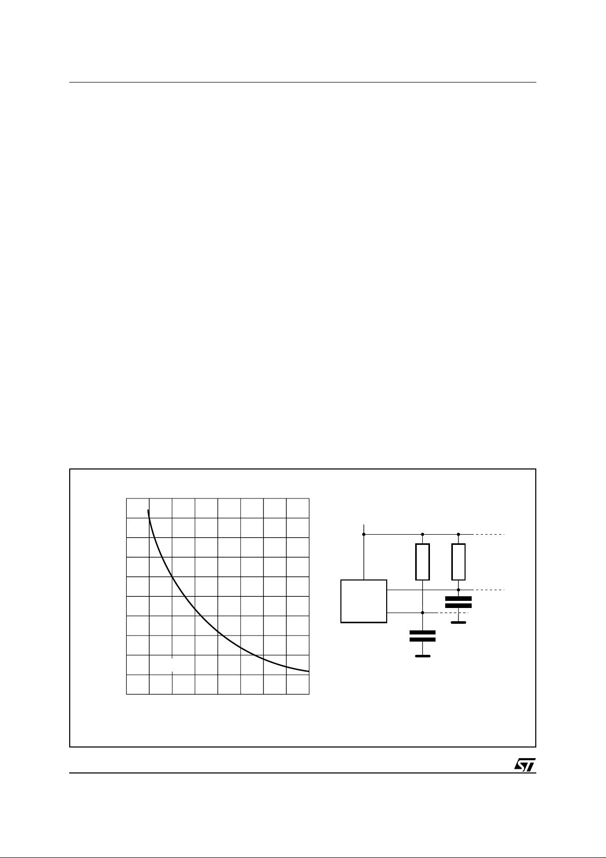
Figure 3. Maximum RL Value versus Bus Capacitance (C
20
16
12
max (kΩ)
L
R
8
4
0
VCC = 5V
100 200 300 400
C
(pF)
BUS
) for an I2C Bus
BUS
V
CC
MASTER
SDA
SCL
R
R
BUS
L
C
BUS
AI01100
L
C
4/16
ST24/25C04, ST24/25W04
T able 5. Input Parameters
(1)
(TA = 25 °C, f = 100 kHz )
Symbol Parameter Test Condition Min Max Unit
C
IN
C
IN
Z
WCL
Z
WCH
t
LP
Note:
1. Sampled only, not 100% tested.
Input Capacitance (SDA) 8 pF
Input Capacitance (other pins) 6 pF
WC Input Impedance (ST24/25W04) VIN ≤ 0.3 V
WC Input Impedance (ST24/25W04) VIN ≥ 0.7 V
Low-pass filter input time constant
(SDA and SCL)
CC
CC
520k
500 k
100 ns
T ab le 6. DC Characteristics
(T
= 0 to 70°C, –20 to 85°C or –40 to 85°C; VCC = 3V to 5.5V or 2.5V to 5.5V)
A
Symbol Parameter Test Condition Min Max Unit
I
I
V
V
V
I
LI
I
LO
I
CC
CC1
CC2
V
V
OL
IL
IH
IL
IH
Input Leakage Current 0V ≤ VIN ≤ V
Output Leakage Current
Supply Current (ST24 series)
Supply Current (ST25 series) V
Supply Current (Standby)
(ST24 series)
Supply Current (Standby)
(ST25 series)
0V ≤ V
SDA in Hi-Z
V
= 5V, fC = 100kHz
CC
(Rise/Fall time < 10ns)
= 2.5V, fC = 100kHz 1 mA
CC
V
= VSS or VCC,
IN
V
CC
V
= VSS or VCC,
IN
= 5V, fC = 100kHz
V
CC
V
= VSS or VCC,
IN
V
CC
V
= VSS or VCC,
IN
= 2.5V, fC = 100kHz
V
CC
≤ VCC
OUT
= 5V
= 2.5V
CC
Input Low Voltage (SCL, SDA) –0.3 0.3 V
Input High Voltage (SCL, SDA) 0.7 V
Input Low Voltage
(E1-E2, PRE, MODE,
WC)
Input High Voltage
(E1-E2, PRE, MODE,
WC)
CC
–0.3 0.5 V
V
– 0.5 VCC + 1 V
CC
2
±
2
±
2mA
100
300
5
50
CC
VCC + 1 V
Output Low Voltage (ST24 series) IOL = 3mA, VCC = 5V 0.4 V
Output Low Voltage (ST25 series) I
= 2.1mA, VCC = 2.5V 0.4 V
OL
Ω
Ω
A
µ
A
µ
A
µ
A
µ
A
µ
A
µ
V
5/16
 Loading...