


MSC1000M
RF & MICROWAVE TRANSISTORS
AVIONICS APPLICATIONS
.RUGGEDIZED VSWR
∞
:1
.INPUT MATCHING
.LOW THERMAL RESISTANCE
.CLASS A OPERATION
.P
DESCRIPTION
The MSC1000M is a Class A, common emitter
transistor with an emitter ballasted Matrix geometry specifically designed for DME/IFF driver applications.
This device is capable of withstanding a ∞:1 load
VSWR at any phase angle under full rated conditions. Low RF thermal resistance and semi-automatic wire bonding techniques ensure high reliability and product consistency.
The MSC1000M is housed in the IMPAC™ package with internal input matching.
= 0.6 W MIN. WITH 10.8 dB GAIN
OUT
ORDER CO DE
MSC1000M
PIN CONNECTION
1. Collector 3. Base
2. Emitter 4. Emitter
.280 2LFL (S058)
epoxy sealed
BRANDING
1000M
ABSOLUTE M AXIMUM RATINGS (T
Symbol Parameter Value Unit
P
DISS
I
C
V
CE
T
J
T
STG
THERMAL DATA
R
TH(j-c)
*Applies only to rated RF amplifier operation
October 1992
Power Dissipation* (See Safe Area) — W
Device Current* 300 mA
Collector-Emitter Bias Voltage* 20 V
Junction Temperature (Pulsed RF Operation) 200
Storage Temperature
Junction-Case Thermal Resistance* 35
case
= 25°C)
65 to +150
−
°
°
°
C/W
C
C
1/5
MSC1000M
ELECTRICAL SPECIFICATIONS (T
case
= 25°C)
STATIC
Symbol Test Condition s
BV
BV
BV
I
CBO
EBO
CEO
CES
h
FE
IC = 1mA IE = 0mA 50 — — V
IE = 1mA IC = 0mA 3.5 — — V
IC = 5mA IB = 0mA 20 — — V
VCE = 28V — — 1.0 mA
VCE = 5V IC = 100mA 15 — 120 —
DYNAMIC
Symbol Test Conditions
P
OUT
G
P
Note: Pulse Widt h=10µSec IC = 120mA
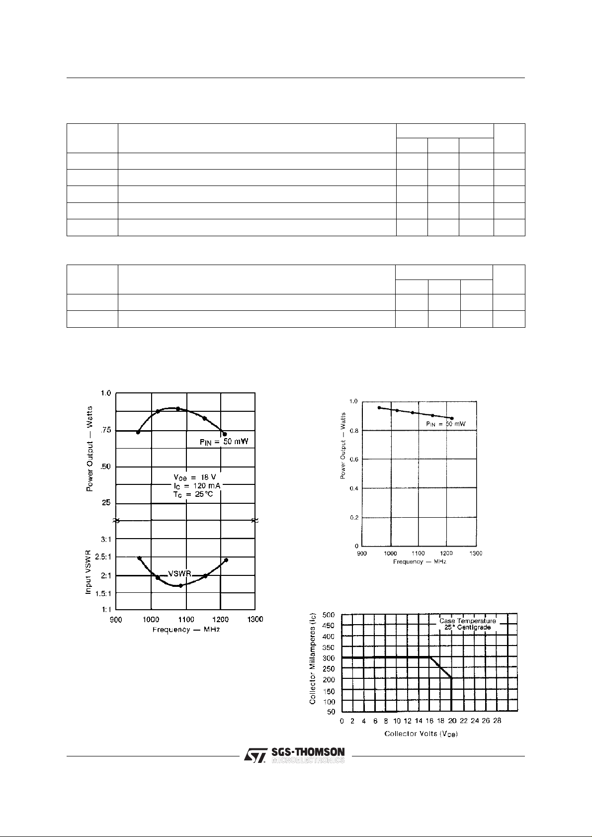
f = 1025 — 1150 MHz PIN = 50 mW VCE = 18 V 0.6 0.85 — W
f = 1025 — 1150 MHz PIN = 50 mW VCE = 18 V 10.8 12.3 — dB
Duty Cycle=1%
TYPICAL PERFORMANCE
BROADBAND POWER AMPLIFIER
Valu e
Min. Typ. Max.
Value
Min. Typ. Max.
NARROWBAND POWER
OUTPUT vs FREQUENCY
Unit
Unit
2/5
MAXIMUM OPERATING AREA for
FORWARD BIAS OPERATION

TYPICAL S−PARAMETERS
MSC1000M
S22S11
S21
VCE = 18 V
IC = 120 mA
Zg = 50 ohms
S12
3/5

MSC1000M
TEST CIRCUIT
Ref.: Dwg No. C127297
All dimensions are in inches.
PACKAGE MECHANICAL DATA
4/5

MSC1000M
Information furnished is believed to be accurate and reliable. However, SGS-THOMSON Microelectronics assumes no responsability for the
consequences of use of such information nor for any infringement of patents or other rights of third parties which may results from its use. No
license is granted by implication or otherwise under any patent or patent rights of SGS-THOMSON Microelectronics. Specifications mentioned
in this publication are subject to change without notice. This publication supersedes and replaces all information previously supplied.
SGS-THOMSON Microelectronics products are not authorized for use as critical components in life support devices or systems without express
written approval of SGS-THOMSON Microelectonics.
© 1994 SGS-THOMSON Microelectronics - All Rights Reserved
Australia - Brazil - France - Germany - Hong Kong - Italy - Japan - Korea - Malaysia - Malta - Morocco - The Netherlands -
Singapore - Spain - Sweden - Switzerland - Taiwan - Thailand - United Kingdom - U.S.A
SGS-THOMSON Microelectronics GROUP OF COMPANIES
5/5
 Loading...