

Page 1
E2D0048-39-22
¡ Semiconductor MSC1157
¡ Semiconductor
This version: Feb. 1999
Previous version: May. 1997
MSC1157
Speaker Drive Amplifier
GENERAL DESCRIPTION
The MSC1157, designed specifically to operate at a low voltage with low current consumption,
is a power amplifier developed for driving a speaker for a voice IC.
The voltage gains can be adjusted over a range of up to ten. The differential output can directly
drive a speaker without any output coupling capacitors. The MSC 1157, because of its ability to
stand by, is ideally suitable for portable equipment applications powered by a battery.
FEATURES
• Low voltage operation : 2.0 to 6.0 V (Single power supply)
• Low current dissipation
Operating current : 1.6mA without load (typ.)
• Standby function : Current dissipation less than 1 mA in standby
• High output current : 350mA peak
• Differential outputs : A speaker can be directly connected between
differential outputs.
• Adjustable gain : Gain can be adjusted by use of an external resistor.
• Package options:
8-pin plastic DIP (DIP8-P-300-2.54) (Product name : MSC1157RS)
8-pin plastic SOP (SOP8-P-250-1.27-K) (Product name : MSC1157MS-K)
Chip
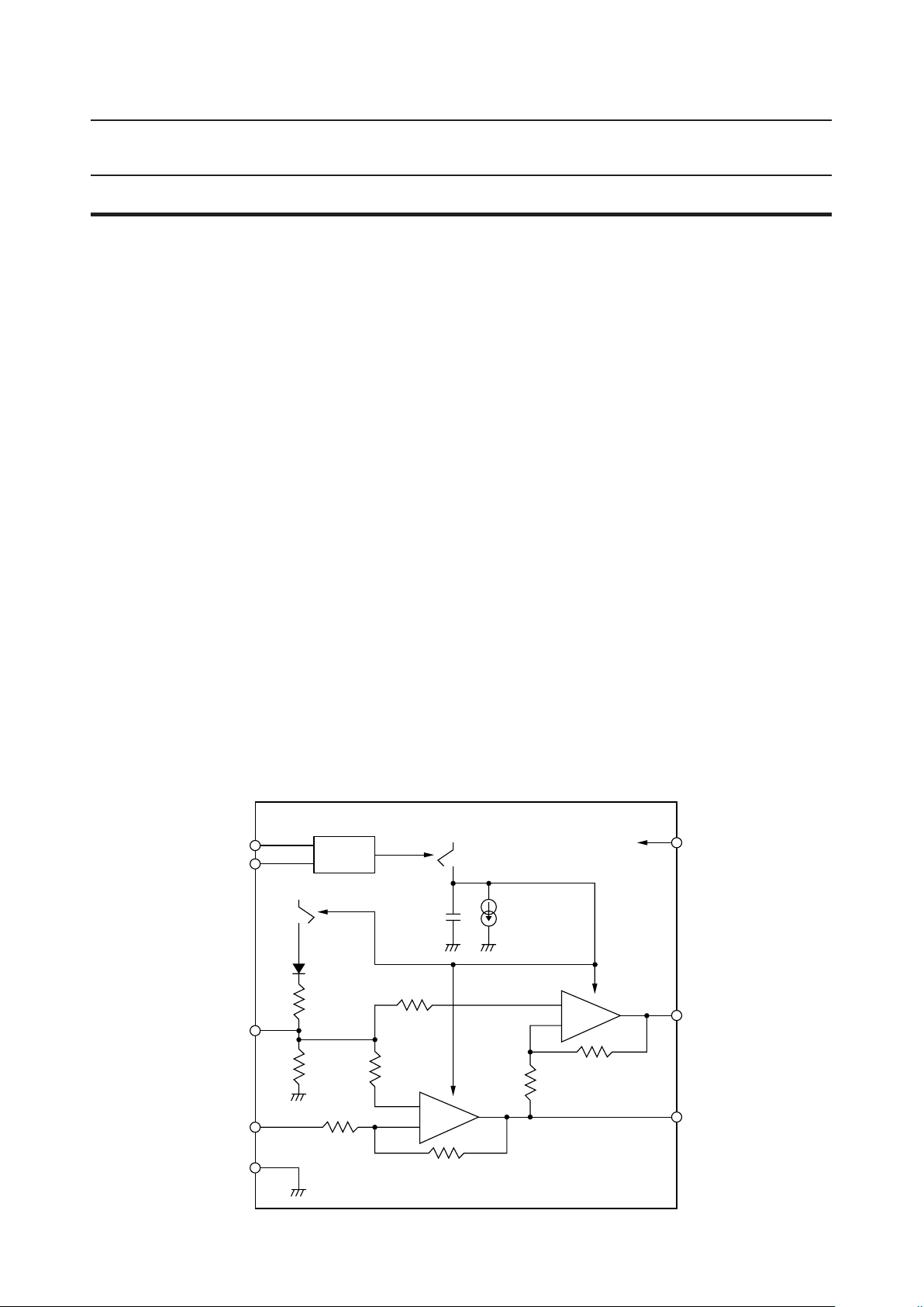
BLOCK DIAGRAM
STBY
SEL
VR
A
IN
GND
V
CC
Logic
V
CC
52 kW50 kW
+
–
20 kW
100 kW
+
–
5 kW
5 kW
V
SP
SP
CC
1/13
Page 2
¡ Semiconductor MSC1157
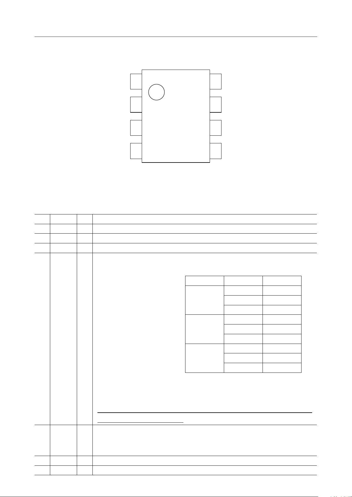
PIN CONFIGURATION (TOP VIEW)
PIN DESCRIPTIONS
Pin
5
4
2
Symbol
V
GND — Ground pin.
Type Description
CC
A
IN
— Power supply pin.
I Signal input pin for analog signal inputs, etc.
VR
A
IN
SP
GND
1
2
3
4
8
SEL
7
STBY
6
SP
5
V
CC
8-Pin Plastic DIP
or
8-Pin Plastic SOP
Digital input pins. Setting these pins configures the standby status. See the table below
for how to set the pins.
7, 8
1
STBY,
SEL
VR O
SEL STBY Status
0 Operation
0 1 Standby
Clock Operation
0 Standby
1 1 Operation
I
Clock Operation
0 Operation
Clock 1 Operation
Clock
Unstable Operation
Applying a clock between 32kHz and 4MHz to either the STBY or the SEL pin leads the IC
to operation status regardless of the status set at the other pin. Applying clocks to both
of the pins at the same time may cause malfunction.
Refer to the section, RECOMMENDED OPERATING CONDITIONS since clock frequencies
are changed by setting the SEL pin.
Bias output pin for internal circuits. This pin is at GND potential during standby.
Connecting a capacitor between VR and the GND pin reduces the pop-up noise at power
on and improves the ripple elimination ratio.
3
6
SP O Speaker output pin. This pin outputs a negative phase with respect to the input signal.
SP O Speaker output pin. This pin outputs a positive phase with respect to the input signal.
2/13
Page 3
¡ Semiconductor MSC1157
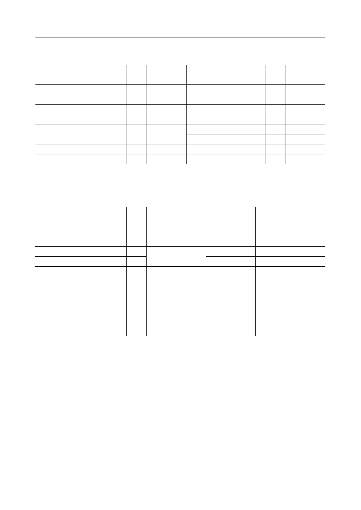
ABSOLUTE MAXIMUM RATINGS
Parameter
Power Supply Voltage V
Symbol
CC
Condition Rating Unit Remark
Ta=25°C –0.3 to +6.5 V V
CC
STBY
Input Voltage V
IN
Ta=25°C –0.3 to VCC+0.3 V
A
IN
, SEL
(*1)
Maximum Output Current I
OMAX
Ta=25°C
±400 mA SP, SP
470 mW DIP type
Power Dissipation P
Junction Temperature
Storage Temperature
T
T
D
jMAX
STG
Ta=25°C
400 mW SOP type
— 125 °C Chip
— –55 to +150 °C
*1 Avoid shorting the output pins (SP and SP) to VCC or GND because the IC may be damaged.
RECOMMENDED OPERATING CONDITIONS
Parameter
Power Supply Voltage V
Load Impedance (*2) RL
Peak Load Current I
"H" Input Voltage V
"L" Input Voltage V
STBY Operating Frequency (*3) f
Operating Temperature Top
Symbol
CC
O-P
IH
IL
STBY
Condition
—
—
—
For STBY and SEL pins
SEL = "L"
At clock input
≥ 2.4 V
V
CC
SEL = "H"
At clock input
≥ 2.4 V
V
CC
—
2.0 6.0 V
8.0 — W
— 350 mA
0.7 V
CC
— 0.3 V
—V
CC
32 k 4.096 M
32 k 1 M
–20 +70 °C
UnitMin. Max.
V
Hz
*2 A speaker of 8 W (standard) or more should be used.
*3 The input of clocks may cause a little noise in output waveforms.
It is recommended to input the DC voltage to inprove voice quality.
3/13
Page 4
¡ Semiconductor MSC1157
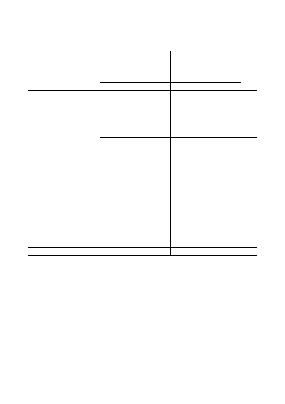
ELECTRICAL CHARACTERISTICS
Unless otherwise specified, Ta=25°C, V
Parameter Symbol Condition UnitMax.Typ.Min.
Input Resistance R
A
IN
Voltage Gain A
IN
A
V1
V2
A
AINÆ(Between SP-SP) 20.512019.46
V3
—kW262014
AINÆSP 14.491413.44
SPÆSP dB+1.580–1.94
VCC=3 V, f=1 kHz
P
OUT1
RL=8 W, THD≥10%
Output Power
VCC=6 V, f=1 kHz
P
OUT2
THD1
Total Harmonic Distortion
THD2
RL=32 W, THD≥10%
V
=3 V, RL=8 W
CC
f=1 kHz, P
=6 V, RL=32 W
V
CC
f=1 kHz, P
=45 mW
OUT
=125 mW
OUT
Ripple Elimination Ratio RR f=1 kHz, C2=4.7 mFdB—4330
Output DC Voltage
(*4)
V
Output Offset Voltage DV
O
signal state
O
In no
Between SP-SP mV±30——
VCC=2 V 0.770.650.53
=6 V 2.732.612.49
V
CC
AIN=VCC or GND
V
OH
I
=–100 mA
OUT
AIN=VCC or GND
Output "L" Voltage
STBY, SEL
Input Current
VR Equivalent Resistance R
Circuit Current During Operation I
Circuit Current During Standby I
V
I
I
CCS
OL
IH
IL
VR
CC
=100 mA
I
OUT
VI=V
CC
VI=GND mA±0.1——
—
VCC=6 V, RL=• mA2.41.61.1
— mA1.0——
CC
=2 to 6 V
CC
mW—178100
mW—440300
%—1.2—
%—0.37—
V
–1.04VCC–1.15Output "H" Voltage
V—V
V0.30.17—
mA±0.1——
kW322518
*4 The typical value of the output voltage in no signal state is determined from the following
equation.
50 kW
VO = (V
CC
– 0.67)
50 kW + 52 kW
4/13
Page 5

¡ Semiconductor MSC1157
APPLICATION CIRCUIT
+
C4 C3
–
Standby
Select
Input
Standby
Input
Audio
Input
C1
SEL
STBY
A
IN
VR
+
C2
–
V
CC
GND
SP
Speaker
SP
• If parasitic capacitance of 60pF or more exists between GND and the speaker output pin SP or
SP, oscillation may occur. Implement the circuit mount design so as to be less than 60pF.
• C1 is the AC coupling capacitor. Cutoff frequency fc on the low frequency side is determined
by the following equation. Choose a value of C1 according to the bandwidth.
1
fc =
(Hz)
2 ¥ p ¥ C1 ¥ 20k
• Choose a value of C2 that is 80 to 100 times as large as that of C1.
• When the standby function is not used, connect the pins STBY and SEL to VCC or GND.
• It is recommended that the capacitor C4 (approximately 0.1mF) having better high frequency
characteristics and the capacitor C3 (approximately 10mF) be placed between the pins VCC and
GND.
5/13
Page 6
¡ Semiconductor MSC1157
GAIN ADJUSTMENT
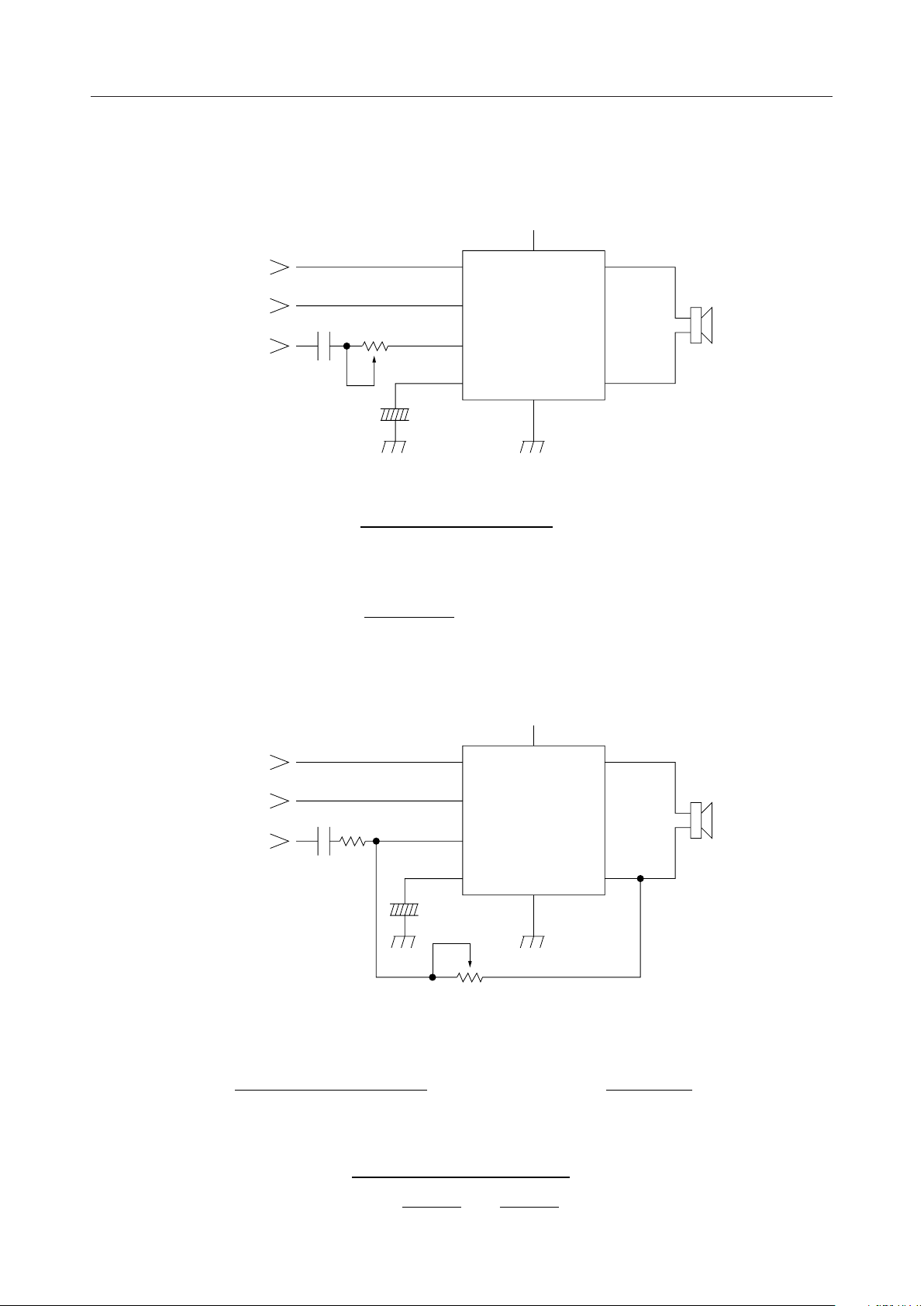
1. Gain Adjustment Using Input Resistance (This approach allows gain adjustment with
fewer external components)
Standby
Select
Input
Standby
Input
Audio
Input
SEL
STBY
C1
R1
A
IN
+
C2
–
VR
V
GND
CC
SP
Speaker
SP
• Cutoff frequency fc on the low frequency side is determined from the equation:
fc =
.
.
1
(Hz)
2 ¥ p ¥ C1 ¥ (R1 + 20k)
• Voltage gain AV1 is determined from the equation:
AV1 =
.
100k
.
(V/V)
R1 + 20k
2. Gain Adjustment Using Feedback Resistance (This approach has the advantage over
the above approach (less noise approach), but the number of components is increased)
Standby
Select
Input
Standby
Input
Audio
Input
SEL
STBY
R1
C1
A
IN
+
–
VR
C2
R2
V
GND
CC
SP
Speaker
SP
• Cutoff frequency fc on the low frequency side is determined from the equation:
fc =
.
.
1
(Hz)
Zin =
.
.
R1 +
2 ¥ p ¥ C1 ¥ Zin
R2 ¥ 20k
(W)
R2 + 120k
• Voltage gain AV1 is determined from the equation:
R1
20k
5
(V/V)
6 ¥ R1
+
R2
AV1 =
.
.
1 +
6/13
Page 7
¡ Semiconductor MSC1157
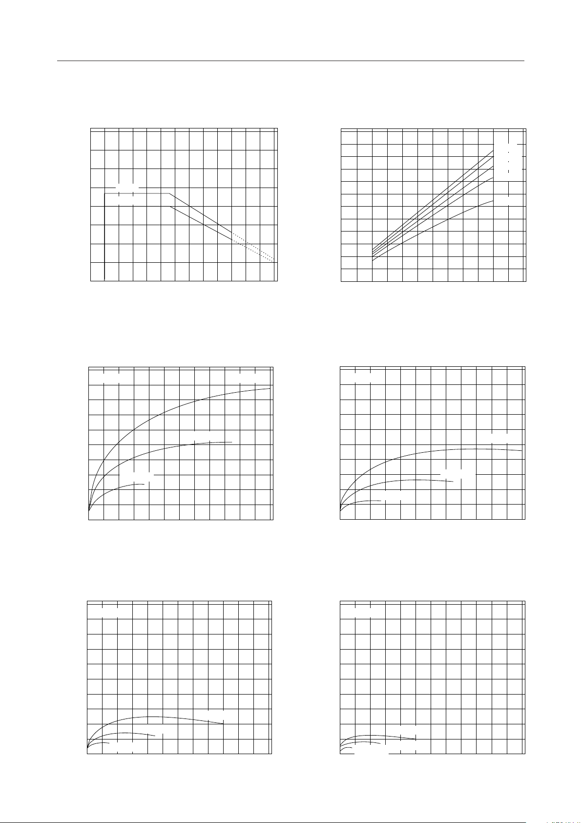
OPERATING CHARACTERISTICS
Power Dissipation vs. Ambient Temperature
800
700
600
[mW]
D
500
400
DIP
SOP
300
Power Dissipation P
200
100
0
-30 -20 -10 0 10 20 30 40 50 60 70 80 90 100
Ambient Temperature Ta [°C]
Power Dissipation vs. Output Power
1000
RL=8W
800
VCC=6.0V
Maxiumum Output Amplitude vs. Voltage Supply
12
RL=•
[V]
OM
10
8
6
RL=64W
RL=32W
RL=16W
RL=8W
4
Maximum Output Amplitude V
2
0
1234567
Supply Voltage VCC [V]
Power Dissipation vs. Output Power
1000
RL=16W
800
[mW]
D
600
VCC=4.5V
400
Power Dissipation P
VCC=3.0V
200
0 100 200 300 400 500 600
Output Power P
OUT
[mW]
Power Dissipation vs. Output Power
1000
RL=32W
800
[mW]
D
600
400
[mW]
D
600
VCC=6.0V
400
Power Dissipation P
200
VCC=3.0V
VCC=4.5V
0 100 200 300 400 500 600
Output Power P
OUT
[mW]
Power Dissipation vs. Output Power
1000
RL=64W
800
[mW]
D
600
400
Power Dissipation P
200
VCC=4.5V
VCC=6.0V
VCC=3.0V
0 100 200 300 400 500 600
Output Power P
OUT
[mW]
Power Dissipation P
200
VCC=3.0V
VCC=6.0V
VCC=4.5V
0 100 200 300 400 500 600
Output Power P
OUT
[mW]
7/13
Page 8
¡ Semiconductor MSC1157
2E-3
1.5E-3
[A]
CC
1E-3
Circuit Current I
5E-4
0 1
2
SP Output
1.8
1.6
1.4
[V]
OL
1.2
1
0.8
0.6
Output "L" Voltage V
0.4
0.2
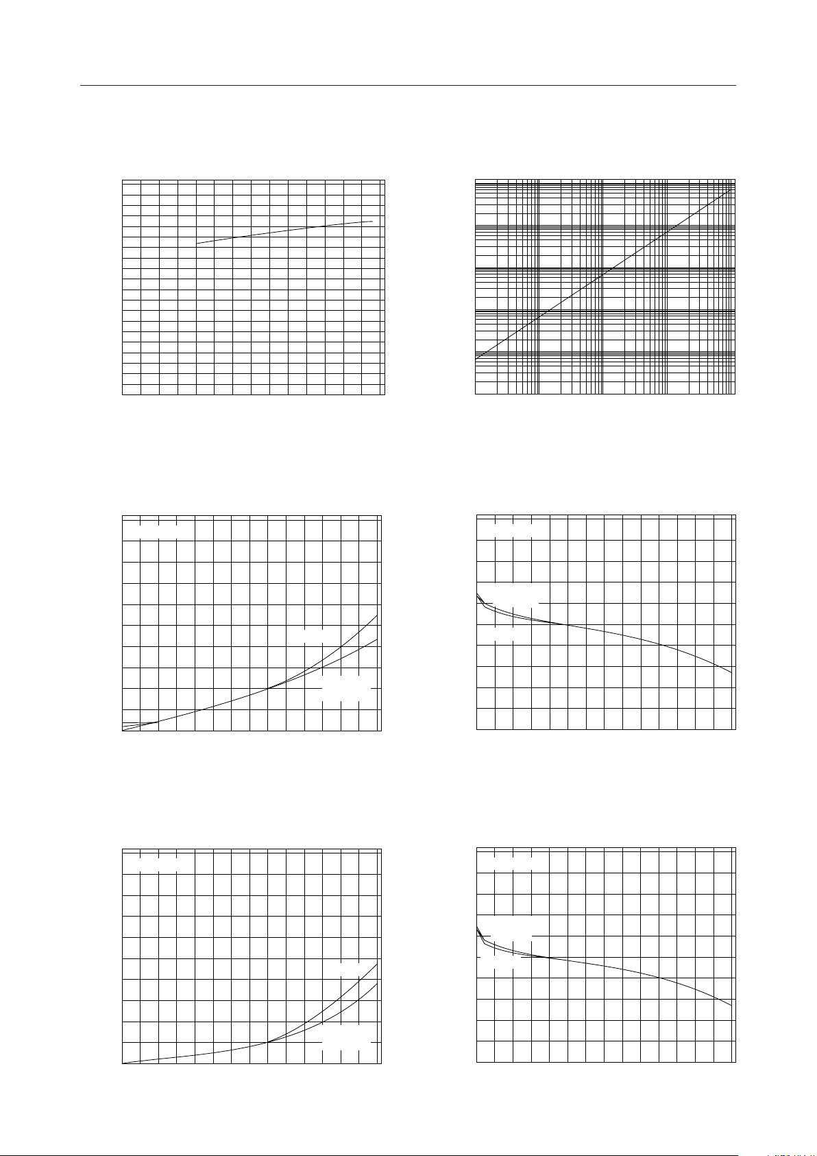
Circuit Current vs. Voltage Supply
234567
Supply Voltage VCC [V]
Output Voltage vs. Load Current
VCC=2.0V
VCC=3.0V
VCC=6.0V
350
300250200150100500
Load Current I
OUT
[mA]
VR Rise Time vs. Capacitor Value (C2)
10000
1000
100
10
1
VR Rise Time (0 to 90%) [ms]
0.1
Output Voltage vs. Load Current
0
SP Output
-0.2
-0.4
) [V]
O
-V
-0.6
CC
VCC=6.0V
(V
VCC=3.0V
-0.8
OH
-1
VCC=2.0V
-1.2
-1.4
-1.6
Output "H" Voltage V
-1.8
-2
Capacitor C2 [mF]
Load Current I
OUT
[mA]
1010.11E-2
100
350
300250200150100500
2
SP Output
1.8
1.6
1.4
[V]
OL
1.2
1
0.8
0.6
Output "L" Voltage V
0.4
0.2
Output Voltage vs. Load Current
Load Current I
OUT
[mA]
VCC=2.0V
VCC=3.0V
VCC=6.0V
300250200150100500
350
0
SP Output
-0.2
-0.4
) [V]
O
-V
-0.6
CC
(V
VCC=6.0V
VCC=3.0V
-0.8
OH
-1
VCC=2.0V
-1.2
-1.4
-1.6
Output "H" Voltage V
-1.8
-2
Output Voltage vs. Load Current
Load Current I
OUT
[mA]
300250200150100500
350
8/13
Page 9
¡ Semiconductor MSC1157
]
]
]
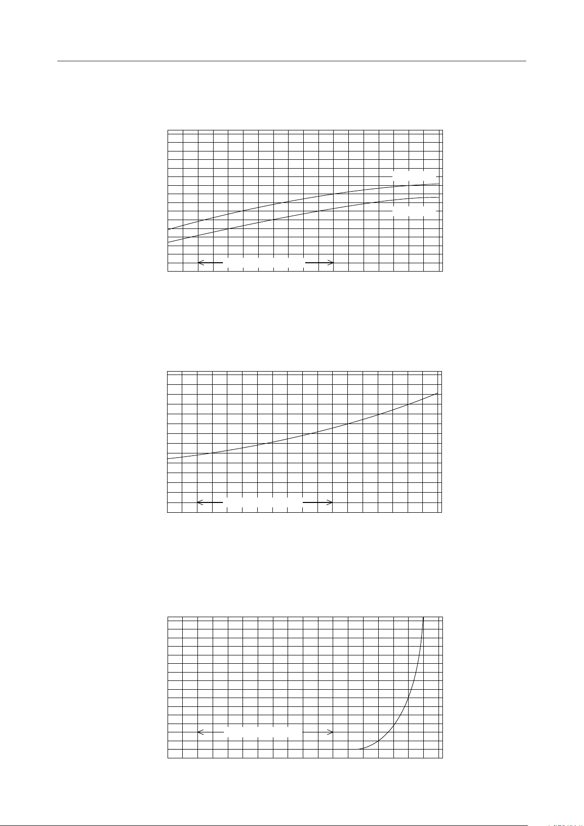
Circuit Curent vs. Ambient Temperature
2.4
2.2
2
1.8
1.6
Circuit Current [mA]
1.4
1.2
1
0.8
64
60
56
52
-20
Range of Ambient Temp.
0 20 40 100 140-40
Ambient Temperature [°C
VR Resistance vs. Ambient Temperature
60 80 120
VCC = 6.0V
VCC = 2.0V
48
VR Resistance [kW]
44
40
36
3
[mA]
CCS
2.6
2.2
1.8
1.4
1
0.6
Circuit Current during standby I
0.2
-20
Range of Ambient Temp.
0 20 40 100 140-40
Circuit Current during Standby vs. Ambient Temperature (V
Range of Ambient Temp.
60 80 120
Ambient Temperature [°C
= 6.0V)
CC
-0.2
-20
0 20 40 100 140-40
Ambient Temperature [°C
60 80 120
9/13
Page 10
¡ Semiconductor MSC1157
]
]
10
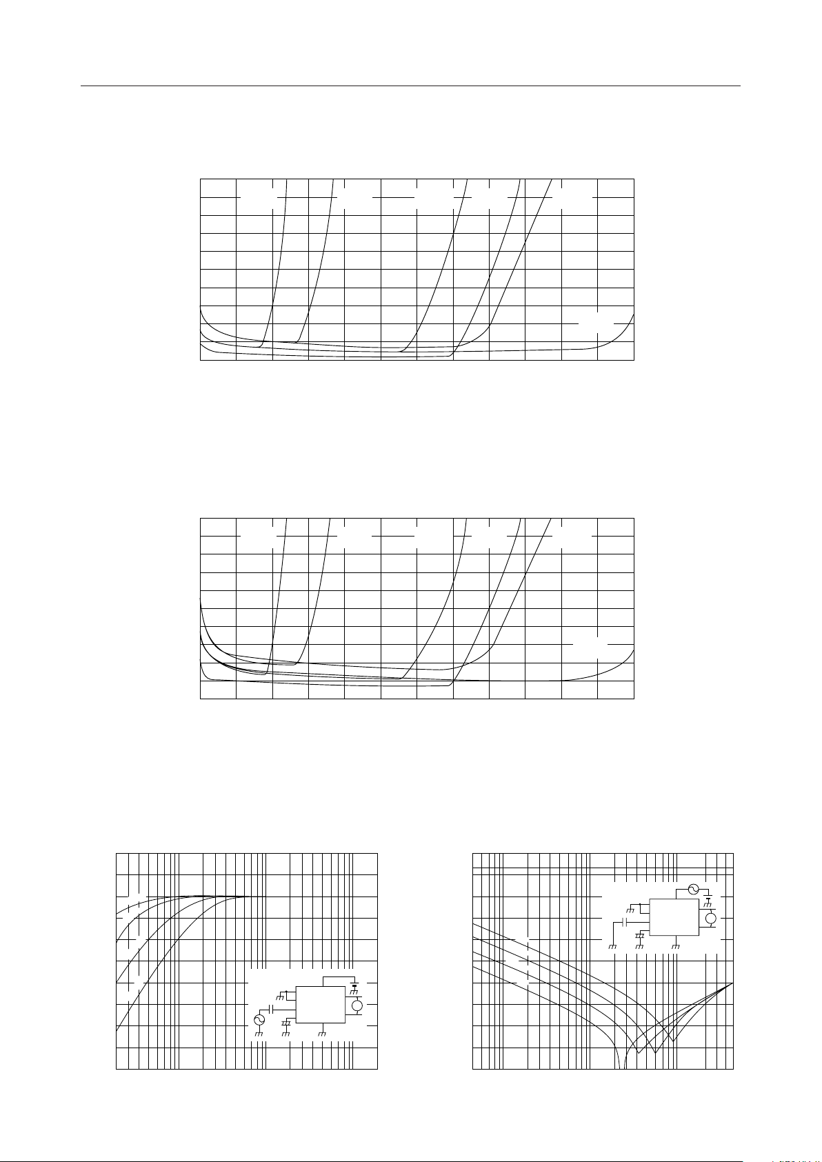
Total Harmonic Distortion vs. Output
VCC=3V
RL=16W
VCC=3V
RL=8W
VCC=4.5V
RL=16W
VCC=6V
RL=32W
VCC=4.5V
RL=8W
5
VCC=6V
RL=16W
Total Harmonic Distortion THD [%]
0
0 100 200 300 400 500 600
Output Power P
OUT
[mW]
Total Harmonic Distortion vs. Output
10
VCC=3V
RL=16W
VCC=3V
RL=8W
VCC=4.5V
RL=16W
VCC=6V
RL=32W
VCC=4.5V
RL=8W
f=1kHz
f=3kHz
26
23
20
C1=0.47
mF
17
C1=0.22
[dB]
14
V3
C1=0.1
11
8
C1=0.047
Voltage Gain A
5
2
-1
-4
20
5
Total Harmonic Distortion THD [%]
0
0 100 200 300 400 500 600
Voltage Gain vs. Frequency
mF
mF
mF
100 1k 10k 20k
Frequency f [Hz
SEL V
C1
STBY
A
IN
VR GND
Vi
CC
SP
SP
Output Power P
V
O
[mW]
OUT
Ripple Elimination Ratio vs. Frequency
20
C2=0 mF
10
0
-10
C
2
=
2
.2
m
-20
-30
-40
F
C
2
=
4
.7
m
F
C
2
=
1
0
m
F
C
2
=
2
2
m
F
-50
Ripple Elimination Ratio RR [dB]
-60
-70
-80
50
100 1k 10k 20k
VCC=6V
RL=16W
Frequency f [Hz
SEL V
STBY
A
IN
VR GND
C2
Vi
CC
SP
V
O
SP
10/13
Page 11
¡ Semiconductor MSC1157
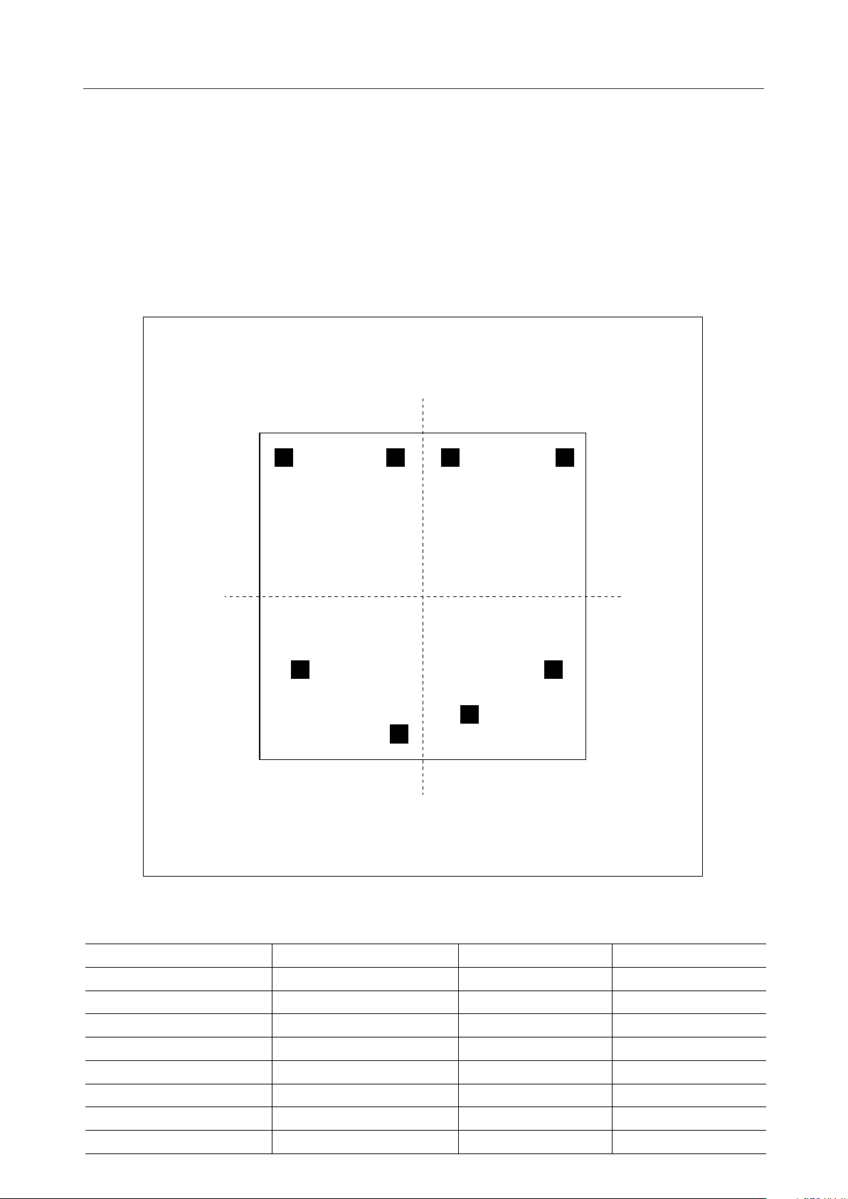
PAD CONFIGURATION
Pad Layout
Chip size : X=2.3mm, Y=2.4mm
Chip thickness : 350±30mm
Pad size (PV aperture) : 110¥110mm
Substrate potential : GND
Pad location diagram
Y-Axis
218 7
3
Pad Coordinates
(Chip center is located at X=0 and Y=0.)
Pad No. Pad Name X-AXIS Y-AXIS
1 VR –133 1035
2A
3 SP –950 –263
4 GND –180 –1027
5V
6 SP 950 –263
7 STBY 985 1035
8 SEL 159 1035
CC
X-Axis
6
5
4
(Unit: µm)
IN
–985 1035
240 –914
11/13
Page 12
¡ Semiconductor MSC1157
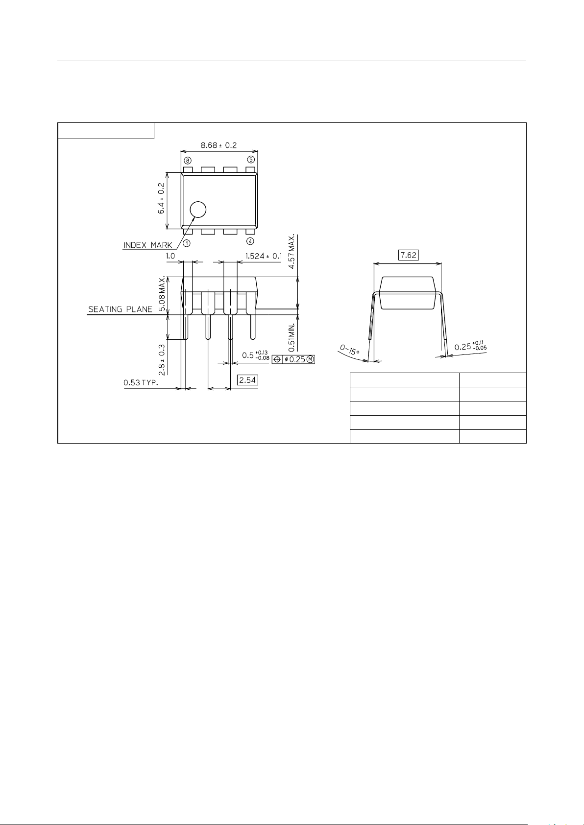
PACKAGE DIMENSIONS
(Unit : mm)
DIP8-P-300-2.54
Package material
Lead frame material
Pin treatment
Solder plate thickness
Package weight (g)
Epoxy resin
42 alloy
Solder plating
5 mm or more
0.46 TYP.
12/13
Page 13
¡ Semiconductor MSC1157
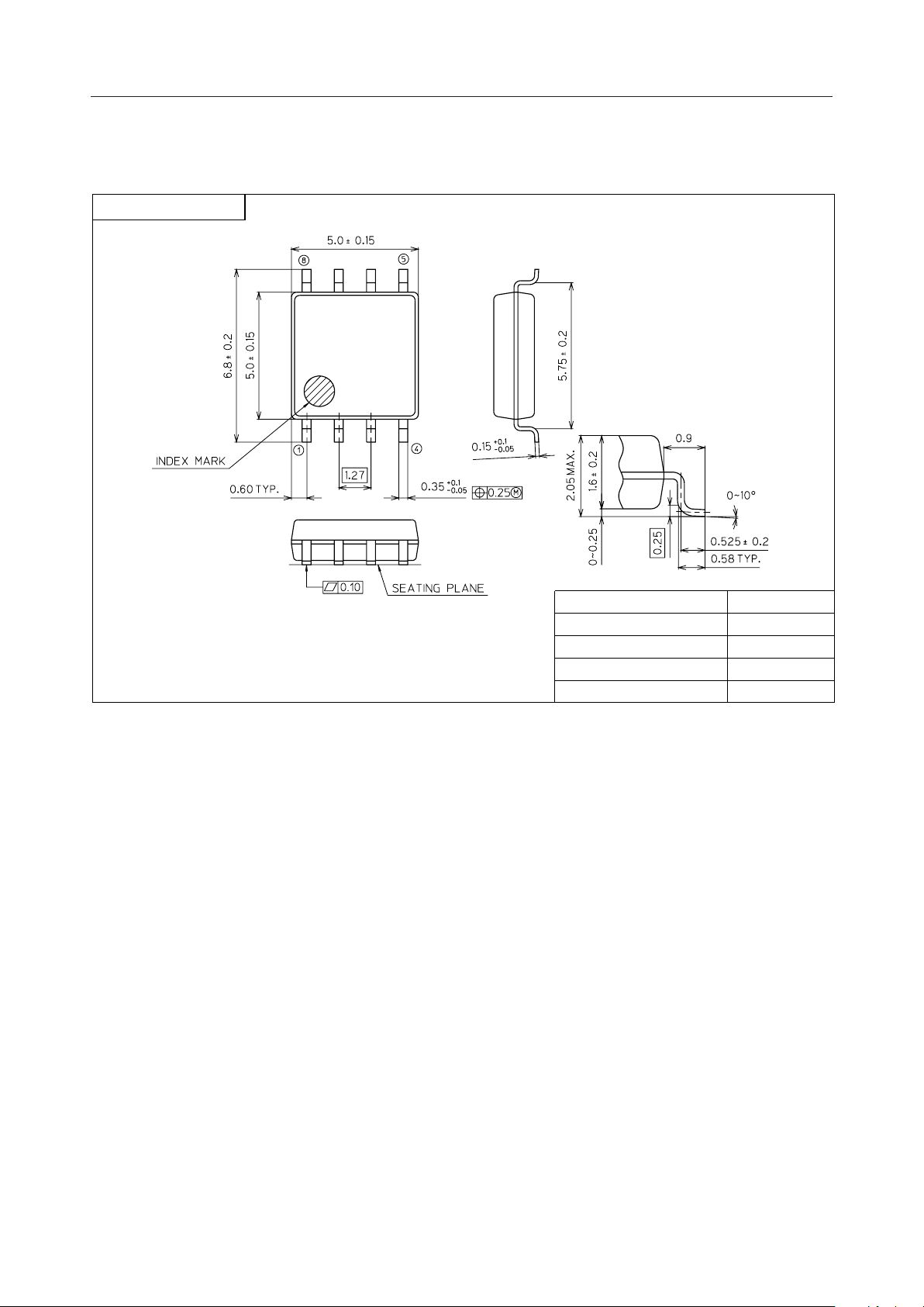
(Unit : mm)
SOP8-P-250-1.27-K
Mirror finish
Package material
Lead frame material
Pin treatment
Solder plate thickness
Package weight (g)
Epoxy resin
42 alloy
Solder plating
5 mm or more
0.10 TYP.
Notes for Mounting the Surface Mount Type Package
The SOP, QFP, TSOP, TQFP, LQFP, SOJ, QFJ (PLCC), SHP, and BGA are surface mount type
packages, which are very susceptible to heat in reflow mounting and humidity absorbed in
storage. Therefore, before you perform reflow mounting, contact Oki’s responsible sales person
on the product name, package name, pin number, package code and desired mounting conditions
(reflow method, temperature and times).
13/13
Page 14

E2Y0002-29-11
NOTICE
1. The information contained herein can change without notice owing to product and/or
technical improvements. Before using the product, please make sure that the information
being referred to is up-to-date.
2. The outline of action and examples for application circuits described herein have been
chosen as an explanation for the standard action and performance of the product. When
planning to use the product, please ensure that the external conditions are reflected in the
actual circuit, assembly, and program designs.
3. When designing your product, please use our product below the specified maximum
ratings and within the specified operating ranges including, but not limited to, operating
voltage, power dissipation, and operating temperature.
4. Oki assumes no responsibility or liability whatsoever for any failure or unusual or
unexpected operation resulting from misuse, neglect, improper installation, repair, alteration
or accident, improper handling, or unusual physical or electrical stress including, but not
limited to, exposure to parameters beyond the specified maximum ratings or operation
outside the specified operating range.
5. Neither indemnity against nor license of a third party’s industrial and intellectual property
right, etc. is granted by us in connection with the use of the product and/or the information
and drawings contained herein. No responsibility is assumed by us for any infringement
of a third party’s right which may result from the use thereof.
6. The products listed in this document are intended for use in general electronics equipment
for commercial applications (e.g., office automation, communication equipment,
measurement equipment, consumer electronics, etc.). These products are not authorized
for use in any system or application that requires special or enhanced quality and reliability
characteristics nor in any system or application where the failure of such system or
application may result in the loss or damage of property, or death or injury to humans.
Such applications include, but are not limited to, traffic and automotive equipment, safety
devices, aerospace equipment, nuclear power control, medical equipment, and life-support
systems.
7. Certain products in this document may need government approval before they can be
exported to particular countries. The purchaser assumes the responsibility of determining
the legality of export of these products and will take appropriate and necessary steps at their
own expense for these.
8. No part of the contents cotained herein may be reprinted or reproduced without our prior
permission.
9. MS-DOS is a registered trademark of Microsoft Corporation.
Copyright 1999 Oki Electric Industry Co., Ltd.
Printed in Japan
 Loading...