

Page 1

E2C0023-27-Y3
¡ Semiconductor MSC1218
¡ Semiconductor
This version: Nov. 1997
Previous version: Jul. 1996
MSC1218
63-Bit Triplex Controller/Driver with Digital Dimming Function
GENERAL DESCRIPTION
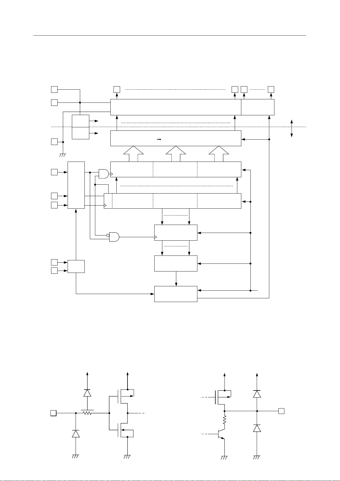
The MSC1218 is a Bi-CMOS driver for 1/3 duty vacuum fluorescent display tube.
It contains a 64-bit shift register, a 63-bit latch, a 10-bit digital dimming circuit, and three grids.
The MSC1218 has only three microcontroller interface signal lines: CS, D-IN, and CLOCK.
The chip select function enables the D-IN and CLOCK lines to be shared with other peripheral
circuits.
FEATURES
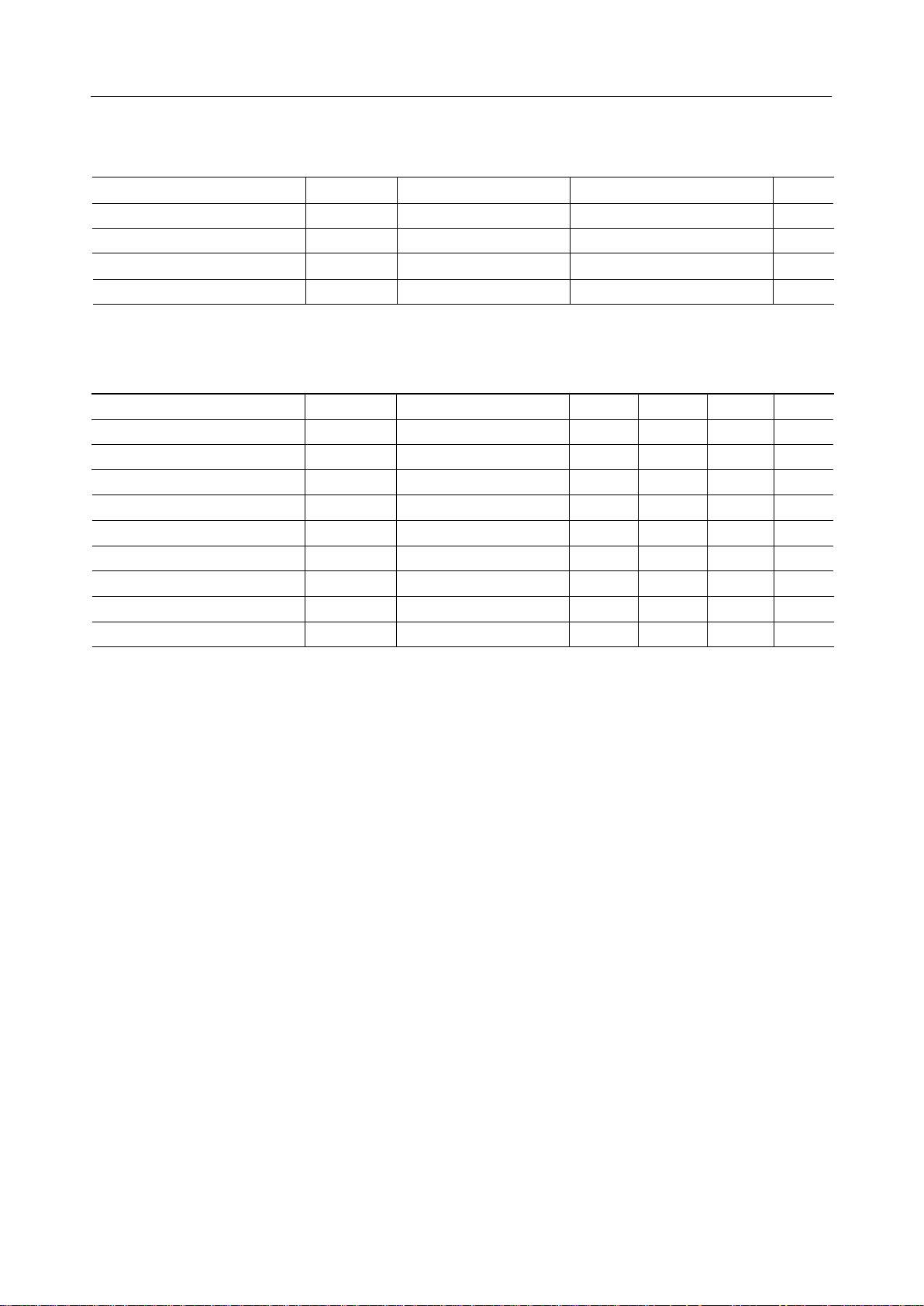
• Power supply Voltage : 8 to 18V (built-in 5V regulator for logic circuit)
• Operating temperature : -40 to +85°C
• 21-segment driver outputs : IOH=–6mA at VOH=VDD–0.8V
• 3-grid driver outputs : IOH=–16mA at VOH=VDD–0.8V
• Built-in digital dimming circuit : 10-bit resolution
• Built-in RC oscillation circuit : External R and C
• Built-in Power-On-Reset circuit
• Package:
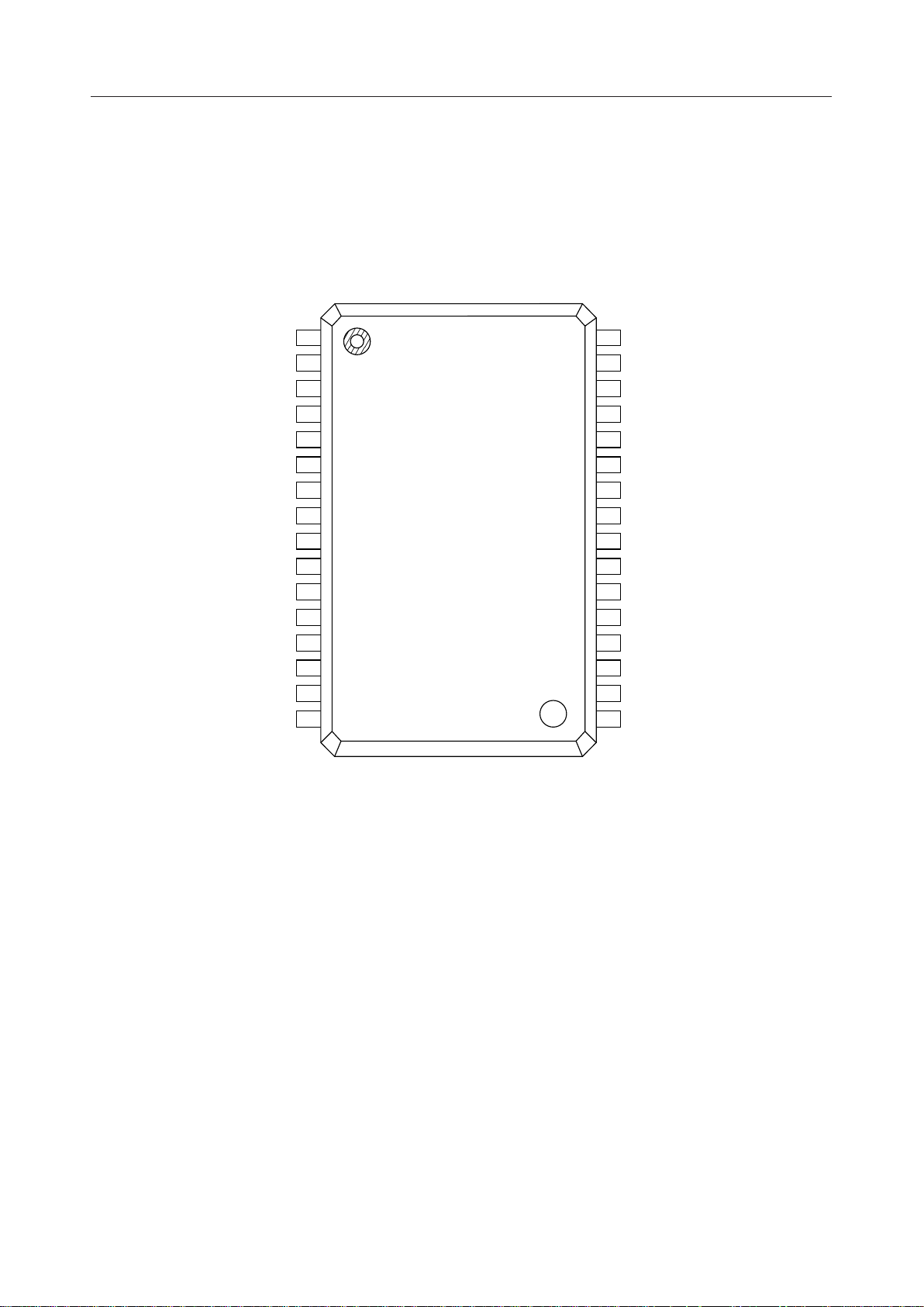
32-pin plastic SSOP(SSOP32-P-430-1.00-K) (Product name: MSC1218GS-K)
1/12
Page 2
¡ Semiconductor MSC1218
BLOCK DIAGRAM
SEG21 SEG1 GRID3 GRID1
V
DD1
V
DD2
5V
REG.
5V
21-bit Segment Driver 3-bit Grid Driver
21-bit data
V
DD
=8 - 18V
GND
CS
DATA-IN
CLOCK
OSC0
OSC1
POR
Control
Circuit
OSC
POR
21
64 63 59 58 49 48
63 21-Segment Control
2121
4363 42 22 21 1
63-bit Latch
63-bit data
64-bit Shift Register
10-bit data
10-bit Latch
10-bit data
10-bit Digital
Diming
Timing
Generator
1
VCC=5.0V
(Regurator)
21
1
POR
64 bits=0: Digital Dimming Mode
64 bits=1: VF Data Input Mode
INPUT AND OUTPUT CONFIGURATION
• Schematic Diagrams of Logic Portion Input
Circuit
INPUT
V
DD
GND
(5V Reg.)
GND
• Schematic Diagrams of Driver Output Circuit
V
GND
DD
V
GND
DD
OUTPUT
2/12
Page 3
¡ Semiconductor MSC1218
PIN CONFIGURATION (TOP VIEW)
SEG 1
SEG 2
SEG 3
SEG 4
SEG 5
SEG 6
SEG 7
SEG 8
SEG 9
SEG10
SEG11
SEG12
SEG13
SEG14
SEG15
SEG16
SEG17
1
2
3
4
5
6
7
8
9
10
11
12
13
14
15
16
32
31
30
29
28
27
26
25
24
23
22
21
20
19
18
17
GRID1
GRID2
GRID3
V
DD2
OSC0
OSC1
GND
DATA-IN
CLOCK
CS
V
DD1
SEG21
SEG20
SEG19
SEG18
32-Pin Plastic SSOP
3/12
Page 4
¡ Semiconductor MSC1218
PIN DESCRIPTIONS
Pin
32,
1 - 20
29 - 31
24
23
27
26
22
21
28
25 —
Symbol Type Decription
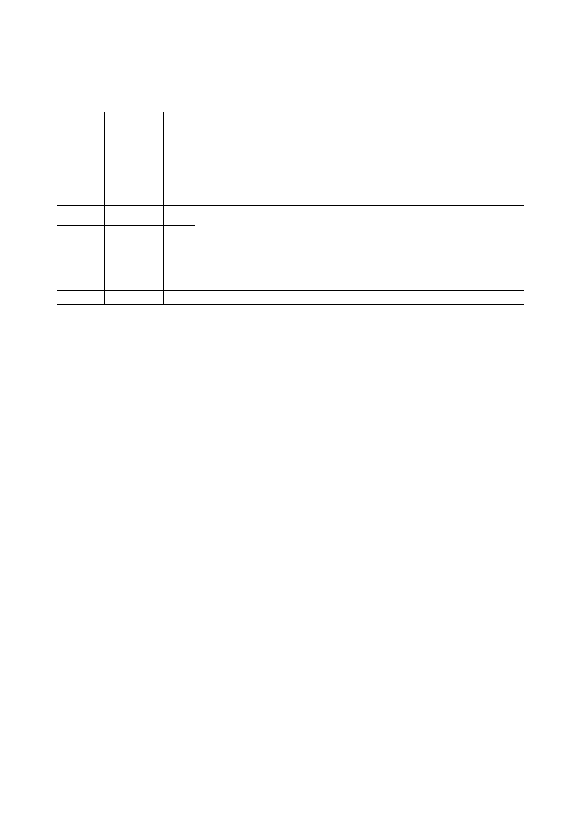
SEG1 - 21 O Output pins for segment signals for driving VF display tube (anode).
GRID1 - 3 O Output pins for grid signals for driving VF display tube (grid).
CLOCK
OSC0
OSC1
CS
V
DD1
V
DD2
GND
ID-IN
Serial data input pin (positive logic).
Shift clock input pin.
I
Serial data shifts at the rising edge of CLOCK.
RC oscillator connecting pins. Oscillation frequency is 3.2MHz.
I
Connect a resistor between the OSC1 and OSC0 pins and a capacitor between
O
the OSC0 pin and the ground.
Chip select input pin. Data transfer is inhibited when this pin is "H".
I
Power supply pins. When using these pins, connect each of them to the power
supply.
—
Ground pin.
4/12
Page 5
¡ Semiconductor MSC1218
ABSOLUTE MAXIMUM RATINGS
Parameter Symbol Rating Unit
Input Voltage
Storage Temperature
Power Dissipation
T
V
V
DD
STG
P
IN
D
Condition
—Power Supply Voltage
All input pins
—
Ta = +85°C
–0.3 to +20 V
–0.3 to +6.0
–65 to +150
400
RECOMMENDED OPERATING CONDITIONS
Parameter Symbol Min. Unit
Power Supply Voltage —
High Level Input Voltage (1)
High Level Input Voltage (2)
Low Level Input Voltage (1)
Low Level Input Voltage (2)
Clock Frequency
Oscillation Frequency
Frame Frequency
Operating Temperature
V
V
V
V
V
f
T
DD
IH1
IH2
IL1
IL2
f
C
OSC
f
FR
op
Condition
—
All inputs except OSC0
OSC0
All inputs except OSC0
OSC0
—
R = 4.7kW, C = 10pF
f
= 3.2MHz
osc
—
Typ.
8V
3.8
4.5
0
0
—
—
—
–40
—
—
—
—
—
3.2
260
—
Max.
18
5.5
5.5
0.8
0.5
250
—
—
85
V
°C
mW
V
V
V
V
kHz
MHz
Hz
°C
5/12
Page 6
¡ Semiconductor MSC1218
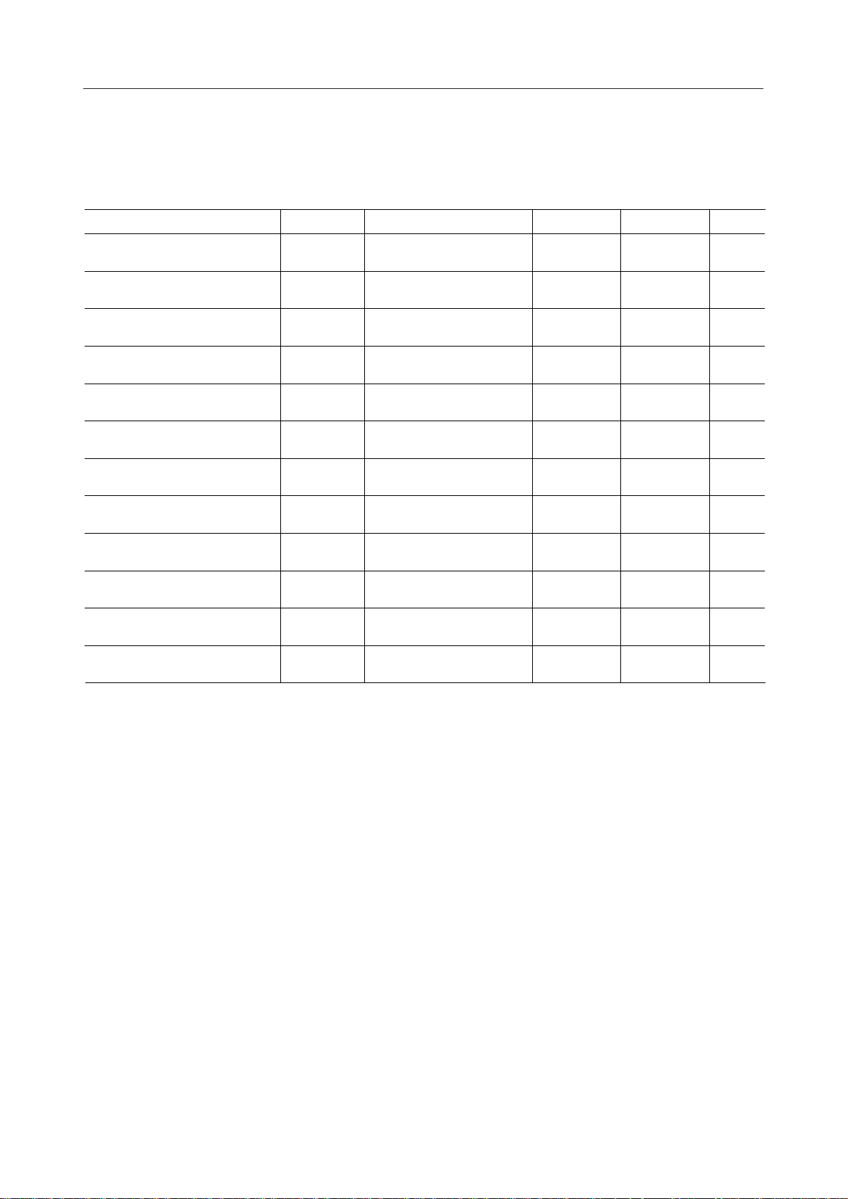
ELECTRICAL CHARACTERISTICS
DC Characteristics
(Ta = –40 to +85˚C, VDD = 8 to 18V (Unless otherwise noted) )
Parameter Symbol
High Level Input Voltage (1)
(All inputs except OSC0)
High Level Input Voltage (2)
(All inputs except OSC0)
Low Level Input Voltage (1)
(OSC0)
Low Level Input Voltage (2)
(OSC0)
High Level Input Current
(All inputs)
Low Level Input Current
(All inputs)
High Level Output Voltage
(SEG1-20)
High Level Output Voltage
(GRID1-3)
Low Level Output Voltage (1)
(SEG1-20, GRID1-3)
Low Level Output Voltage (2)
(SEG1-20, GRID1-3)
Low Level Output Voltage (3)
(SEG1-20, GRID1-3)
Current Consumption
V
V
V
V
V
V
V
V
V
V
IH1
IH2
IL1
IL2
I
IH
I
IL
OH1
OH2
OL1
OL2
OL3
DD
Condition
—
—
External input only
= 5.0V
V
IH1
= 0.0V
V
IL
= 9.5V
V
DD
I
= –6mA
OH1
V
= 9.5V
DD
I
= –16mA
OH2
= 9.5V
V
DD
I
= 500mA
OL1
= 9.5V
V
DD
I
= 200mA
OL2
= 9.5V
V
DD
I
= 2mA
OL3
f
= 3.2MHz
OSC
No load
Min. UnitMax.
0.0
0.0
–5
–5
–0.8
V
DD
V
–0.8
DD
—
—
—
—
5.53.8
0.8
0.8
5
5
—
—
2
1
0.3
10
V
VExternal input only 5.54.5
V
V
mA
mA
V
V
V
V
V
V
6/12
Page 7
¡ Semiconductor MSC1218
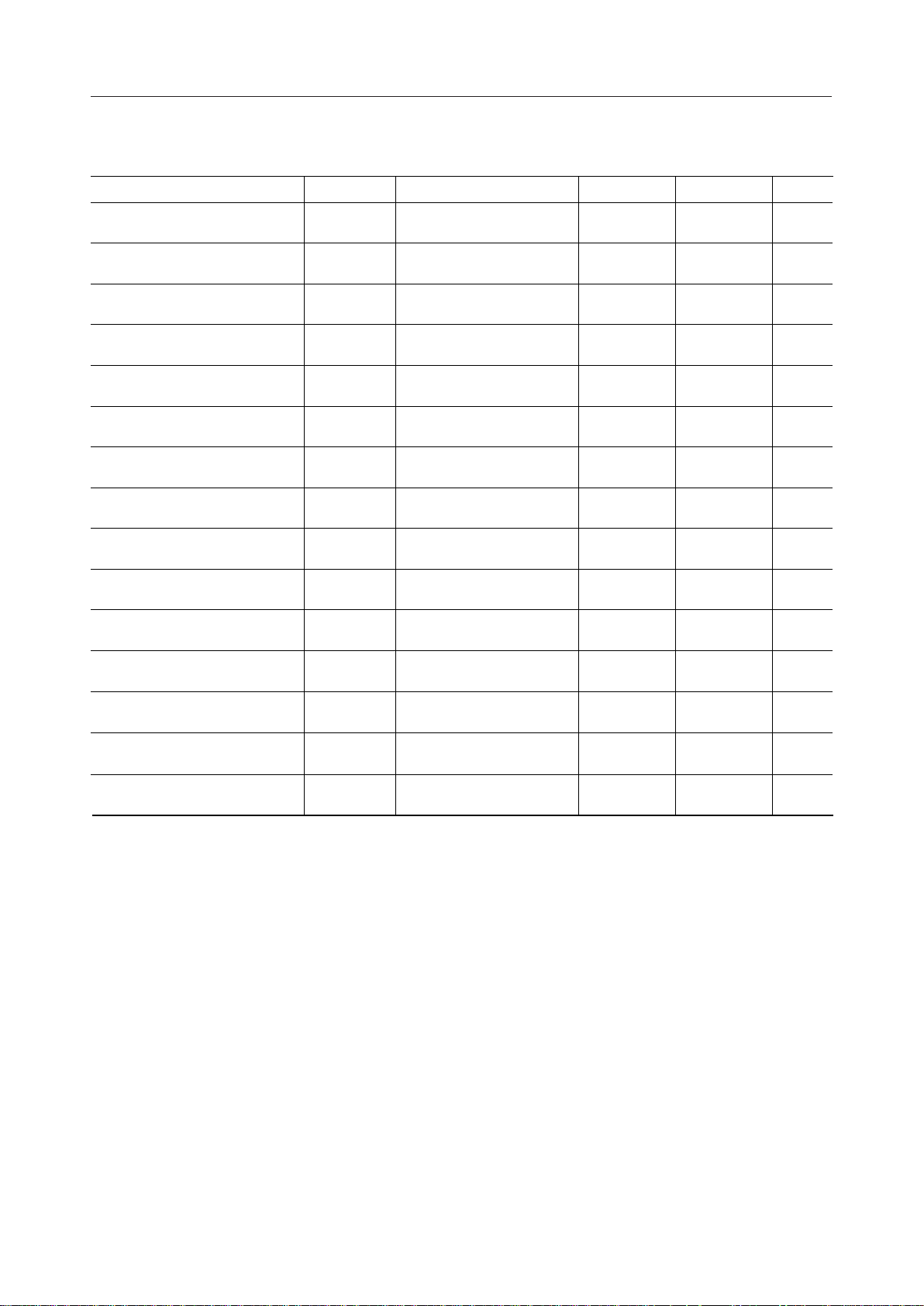
AC Characteristics
(Ta = –40 to +85˚C, VDD = 8 to 18V (Unless otherwise noted) )
Parameter Symbol
Condition
Min. UnitMax.
External Input Frequency to OSC0
Clock Frequency
Clock Pulse Width
Data Setup Time
Data Hold Time
CS Pulse Width
CS Off Time
CS Setup Time
(CS – Clock)
CS Hold Time
(Clock – CS)
CS–All Output Delay Time
Slew Rate (All Drivers)
f
OSC
f
OSCI
f
t
CW
t
DS
t
DH
t
CSW
t
CSL
t
CSS
t
CSH
t
ODS
t
R=4.7kW, C=10pFOscillation Frequency
4.42
MHz
MHzExternal input only 3.72.7
C
—
—
—
—
—
—
—
—
=100pF
C
I
C
=100pF
R
t=20% to 80% or 80% to 20%
I
—
1.3
1
200
8
32
2
2
—
—
250
—
—
—
—
—
—
—
8
5
kHz
ms
ms
ns
ms
ms
ms
ms
ms
ms
Power – CS Time at Power-on
Hold Time at Power-off
Rise Time at Power-on
t
PCS
t
POF
t
PRZ
—
When mounted on the unit
= 0.0V
V
DD
When mounted on the unit
300
5
—
—
—
100
ms
ms
ms
7/12
Page 8
¡ Semiconductor MSC1218
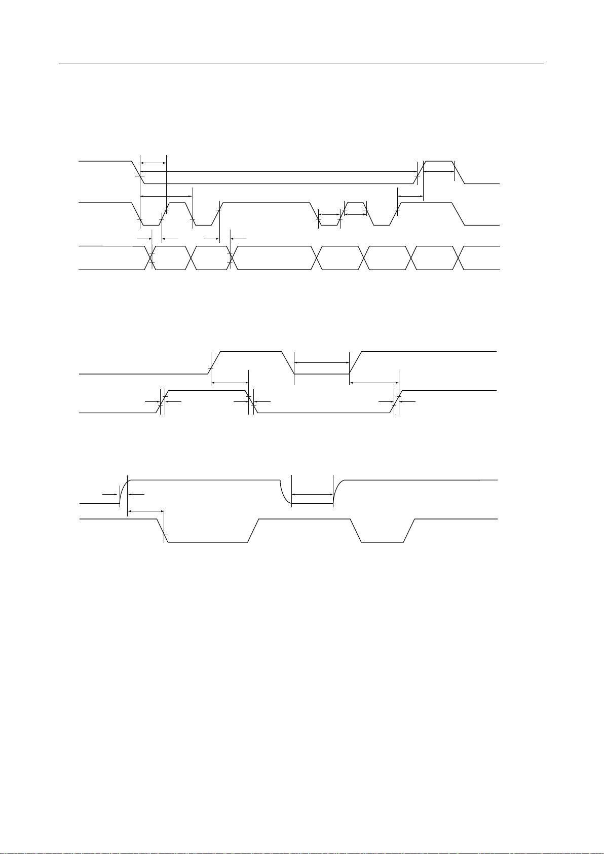
TIMING DIAGRAM
1) Data Input Timing
t
CS
CLOCK
CSS
f
C
t
DS
t
CSW
t
CSL
-3.8V
-0.8V
t
CSH
t
CW
t
t
DH
CW
-3.8V
-0.8V
DATA-IN
VALID VALID VALID VALID
2) Data Output Timing
CS
SEG1-21,
t
R
GRID1-3
3) Power-on Timing
t
V
CS
DD
PRZ
t
PCS
t
ODS
-3.8V
-0.8V
t
CSW
t
ODS
t
R
t
R
-3.8V
-0.8V
-80%
-20%
t
POF
-80%V
DD
-0.0V
-3.8V
-0.8V
8/12
Page 9
¡ Semiconductor MSC1218
FUNCTIONAL DESCRIPTION
l Power-on Reset
The built-in Power-on-Reset (POR) circuit initializes the internal circuits when power is applied.
The following condition is established after POR.
1) Contents of the shift register and latches are "0".
2) Duty cycle of digital dimming is set to "0".
3) All the outputs are OFF.
l Function Mode
The function mode is selected according to the output of the last bit of the shift register.
The function modes are as follows.
M0 (Last bit) Function
0
1
Digital dimming data input mode
Display data input mode
l Digital Dimming Data Input
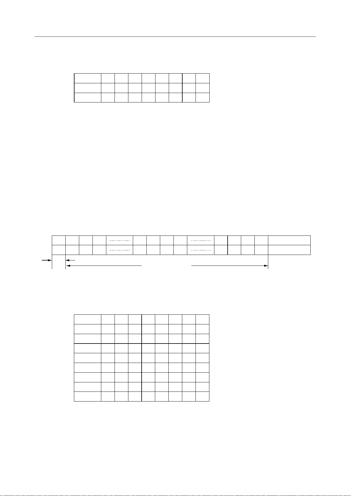
When M0="0", the digital dimming data input mode is selected and the input data length is 16
bits.
The digital dimming data input is valid only when the low level is applied to the CS pin.
The digital dimming data that was input to DATA-IN is input into the shift register at the rising
edge of the CLOCK.
Data is automatically loaded to the latches from the shift register at the rising edge of CS.
The digital dimming data consists of 10 bits.
The output duty varies from 0/1024 (0%) to 1016/1624 (99%) for each grid.
The 10-bit digital dimming data should be input starting with the LSB.
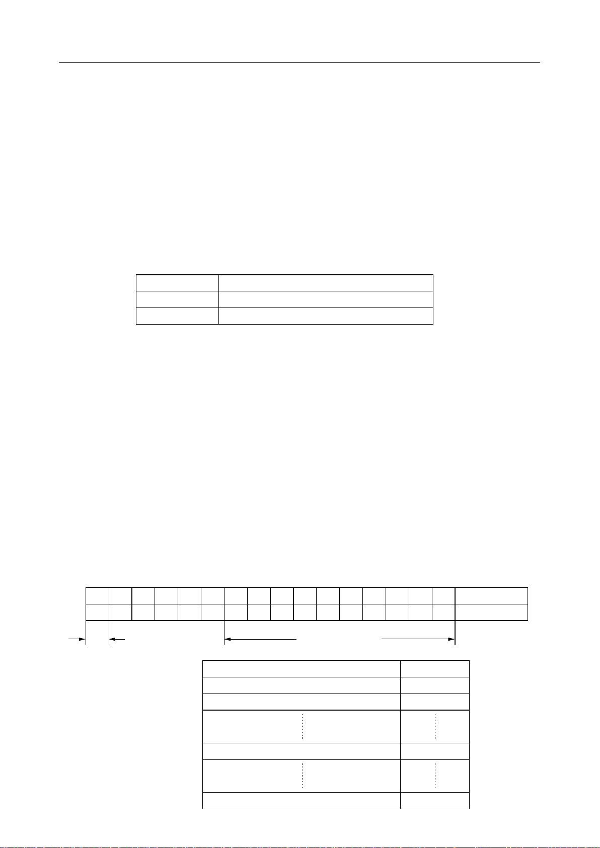
[Data Configuration]
Digital dimming data input mode
Input data: 16bits
Digital dimming data: 10 bits
Mode selector: 1 bit
16M015*14*13*12*11*10
D109D98D87D76D65D54D43D32D21D1
MSB LSB
MODE DATA DIMMING DATA
BIT (First In)
INPUT DATA
INPUT DATA (LSB)(MSB)
DUTY CYCLE
0000000000
1000000000
1016/1024
0001111111
1016/1024
1111111111
0/1024
1/1024
9/12
Page 10
¡ Semiconductor MSC1218
[Input Configuration]
l Dimming data
BYTE1B7D8B6D7B5D6B4D5B3D7B2D3B1D2B0
D1
2 M0*****D10D9
l Display Data Input
When M0="1", the display data input mode is selected and the input data length is 16 bits.
The display data input is valid only when the low level is applied to the CS pin.
The display data that was input to DATA-IN is input into the shift register at the rising edge of
CLOCK.
The data is automatically loaded to the latched from the shift register at the rising edge of CS.
[Data Configuration]
Display data input mode
Input data: 64bits
Display data: 63 bits
Mode selector: 1 bit
64M063
D6362D6261D61
MODE DATA
[Input Configuration]
Display data
BYTE1B7D8B6D7B5D6B4D5B3D7B2D3B1D2B0
2 D16 D10 D9
3 D24 D18 D17
4 D32 D26 D25
5 D40 D34 D33
6 D48 D42 D41
7 D56 D50 D49
8 D64 D58 D57
33
D3332D3231D3130D30
DISPLAY DATA
D15 D14 D13 D12 D11
D23 D22 D21 D20 D19
D31 D30 D29 D28 D27
D39 D38 D37 D36 D35
D47 D46 D45 D44 D43
D55 D54 D53 D52 D51
D63 D62 D61 D60 D59
D1
4D43D32D21
D1
BIT (First In)
INPUT DATA
10/12
Page 11
¡ Semiconductor MSC1218
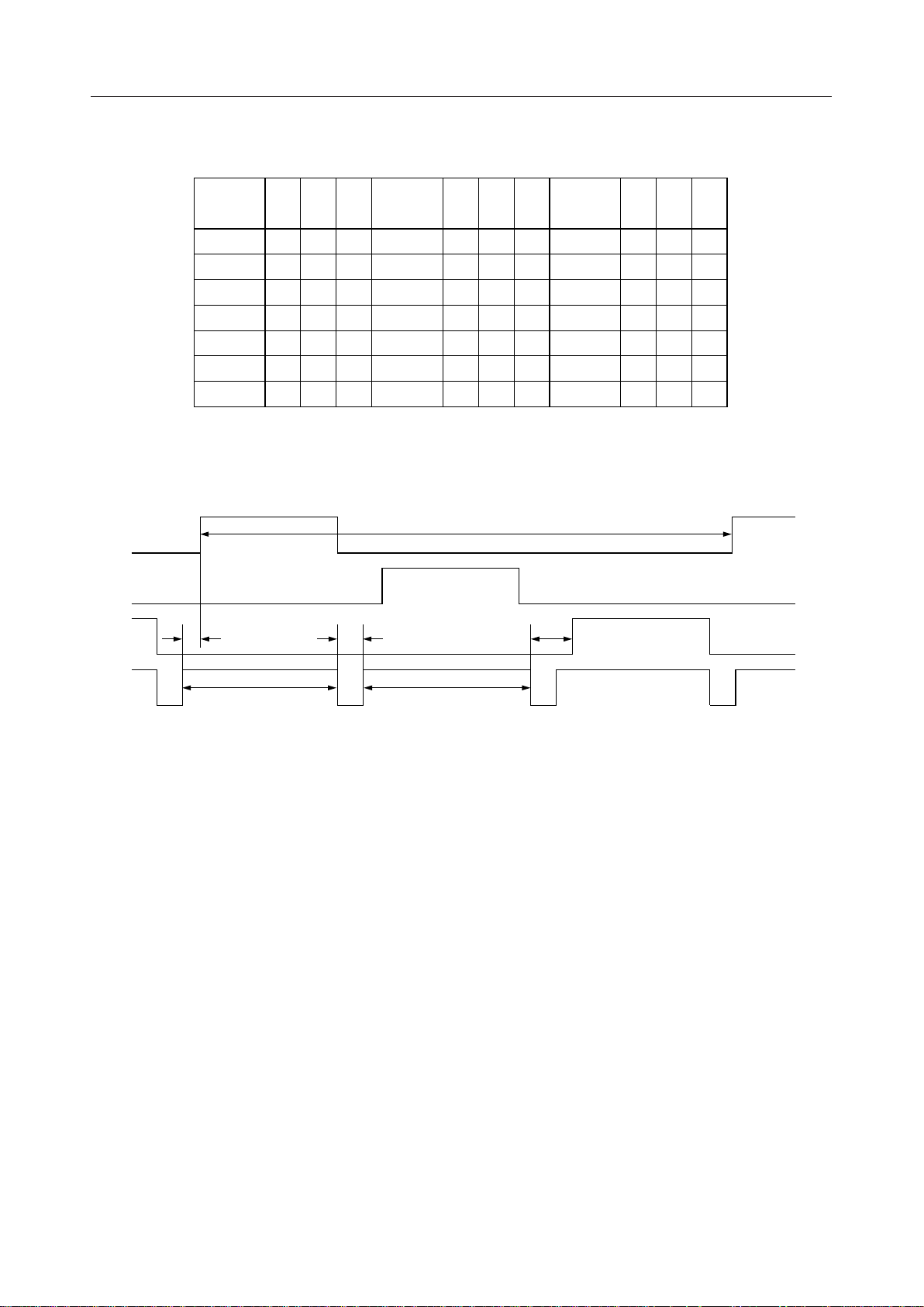
[Configuration of Segment output and Shift Register]
GRID
GRID
Segment
SEG1
SEG2 D2
SEG3 D3
SEG4 D4
SEG5 D5
SEG6 D6
SEG7 D7
1
D1
GRID
2
3
D22
D43
D23 D44
D24 D45
D25 D46
D26 D47
D27 D48
D28 D49
Segment
SEG8
SEG9 D9
SEG10 D10
SEG11 D11
SEG12 D12
SEG13 D13
SEG14 D14
GRID
1
D8
GRID
GRID
2
D29
D50
D30 D51
D31 D52
D32 D53
D33 D54
D34 D55
D35 D56
Segment
3
SEG15
SEG16 D16
SEG17 D17
SEG18 D18
SEG19 D19
SEG20 D20
SEG21 D21
GRID
1
D15
GRID
GRID
2
D36
D57
D37 D58
D38 D59
D39 D60
D40 D61
D41 D62
D42 D63
3
Output Timing *1bit time=4f
GRID1
GRID2
GRID3
GRID1-21
3bit times 5bit times 8bit times
1019bit times 1024bit times
OSC
3072bit times (1 display cycle)
V
DD
–GND
–V
DD
GND
–V
DD
GND
V
DD
–GND
11/12
Page 12
¡ Semiconductor MSC1218
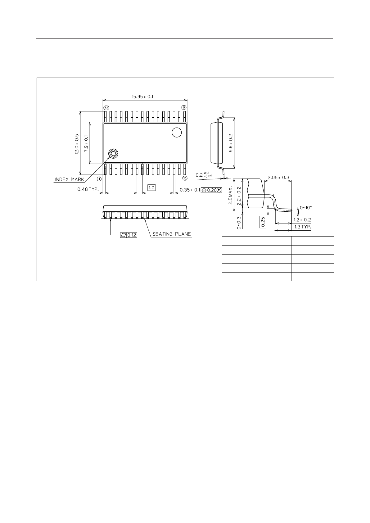
PACKAGE DIMENSIONS
(Unit : mm)
SSOP32-P-430-1.00-K
Mirror finish
Package material
Lead frame material
Pin treatment
Solder plate thickness
Package weight (g)
Epoxy resin
42 alloy
Solder plating
5 mm or more
0.60 TYP.
Notes for Mounting the Surface Mount Type Package
The SOP, QFP, TSOP, SOJ, QFJ (PLCC), SHP and BGA are surface mount type packages, which
are very susceptible to heat in reflow mounting and humidity absorbed in storage.
Therefore, before you perform reflow mounting, contact Oki’s responsible sales person for the
product name, package name, pin number, package code and desired mounting conditions
(reflow method, temperature and times).
12/12
 Loading...