

Page 1

E2C0034-27-Y5
¡ Semiconductor MSC1162A
¡ Semiconductor
This version: Nov. 1997
Previous version: Jul. 1996
MSC1162A
40-Bit Vacuum Fluorescent Display Tube Grid/Anode Driver
GENERAL DESCRIPTION
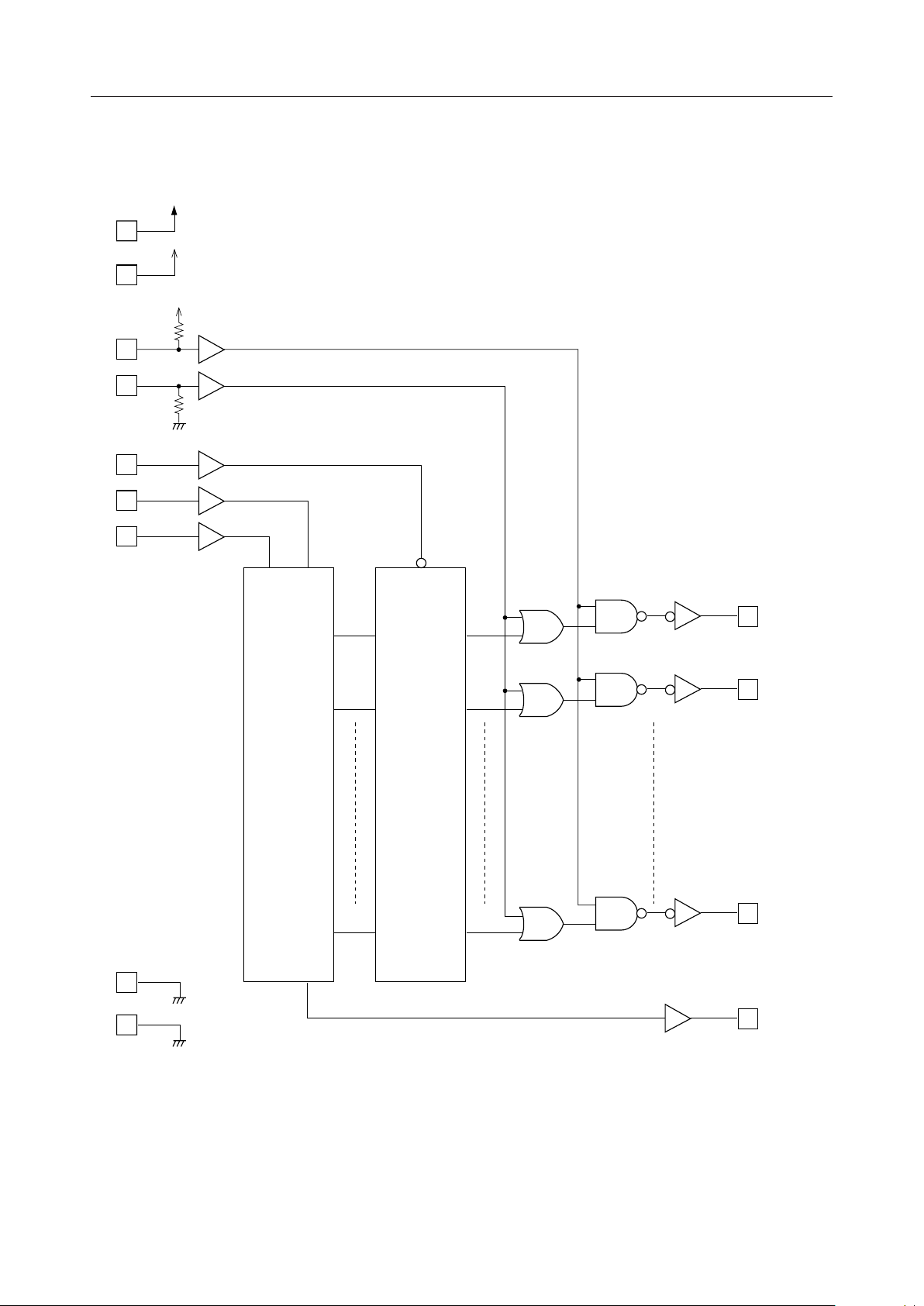
The MSC1162A is a monolithic IC designed for directly driving the grid and anode of the vacuum
fluorescent display tube. The device contains a 40-bit bidirectional shift register, a 40-bit latch
circuit, and 40-output circuit on a single chip.
Display data is serially stored in the shift register at the rising edge of a clock pulse.
Setting the CL pin low allows all the driver outputs to be driven low, which makes it possible to
set the display blanking.
Also, setting both of the CL and CHG pins high allows all the driver outputs to be driven high,
which provides the easy testing of all lights after final assembly of a VFD tube panel.
The MSC1162A is compatible with the MSC1162.
FEATURES
• Logic Supply Voltage (VCC): 5V
• Driver Supply Voltage (VHV): 65V
• Driver Output Current
I
OHVH1
I
OHVH2
I
OHVL
• Directly connected to VFD tube without pull-down resistors
• Data Transfer Speed: 4MHz
• Package :
60-pin plastic SSOP (SSOP60-P-700-0.65-BK) (Product name : MSC1162AGS-BK)
(Only one driver output : "H") : –40mA
(All the driver outputs : "H") : –2mA
:1mA
1/14
Page 2
¡ Semiconductor MSC1162A
BLOCK DIAGRAM
V
HV
V
CC
V
CC
CL
CHG
LS
DIN
CLK
GND1
CSI
PO1
PO2
40-Bit Bi-
directional
Shift
Register
PO40 O-40I-40
SO
I-1
I-2
HVO1
O-1
HVO2
O-2
40-Bit
Latch
HVO40
GND2
DOUT
2/14
Page 3
¡ Semiconductor MSC1162A
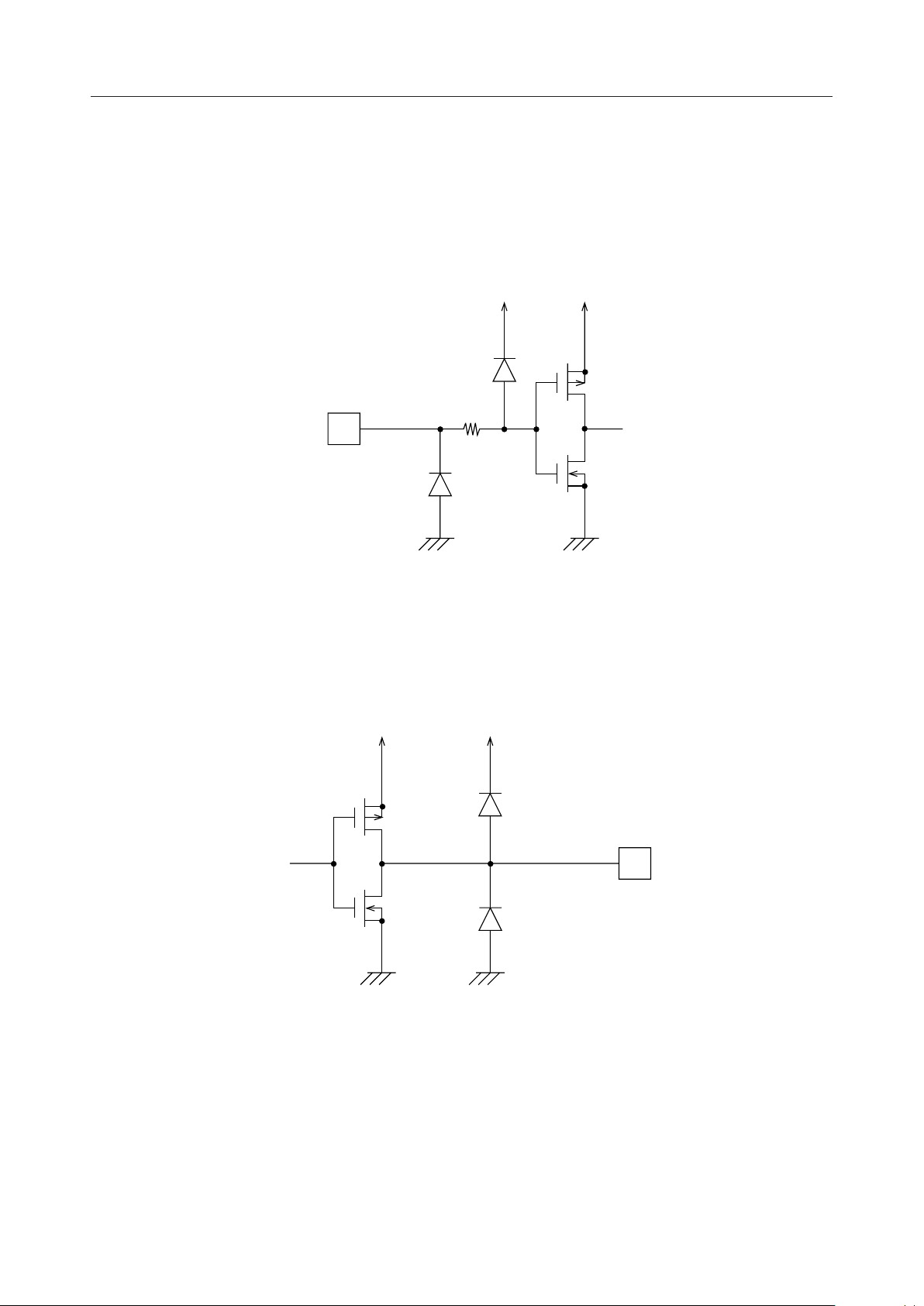
INPUT AND OUTPUT CONFIGURATION
Schematic Diagrams of Logic portion Input/Output Circuits and Driver Output Circuits
Input Pin
Output Pin
INPUT
V
CC
V
CC
V
CC
GND1 GND2
V
CC
GND2 GND1
DOUT
3/14
Page 4
¡ Semiconductor MSC1162A
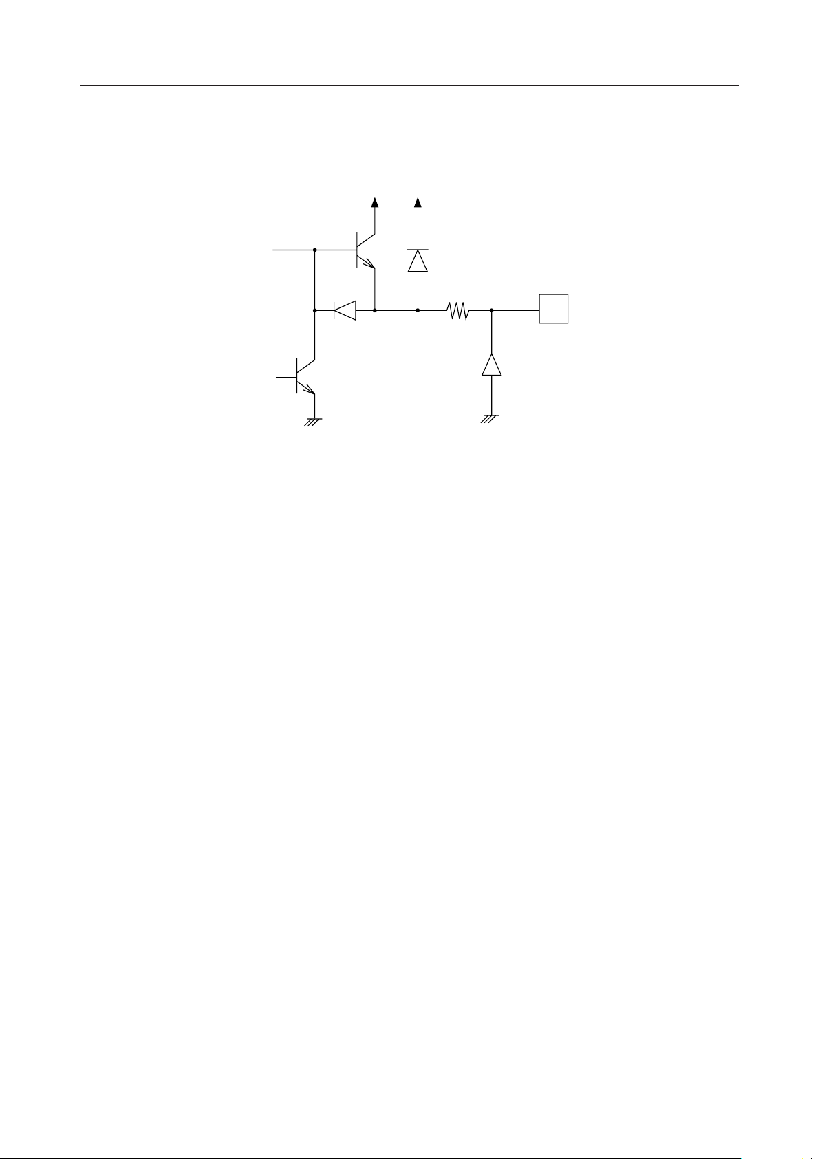
Driver Output Circuit
V
GND 1
HV
V
HV
Output
GND 1
4/14
Page 5
¡ Semiconductor MSC1162A
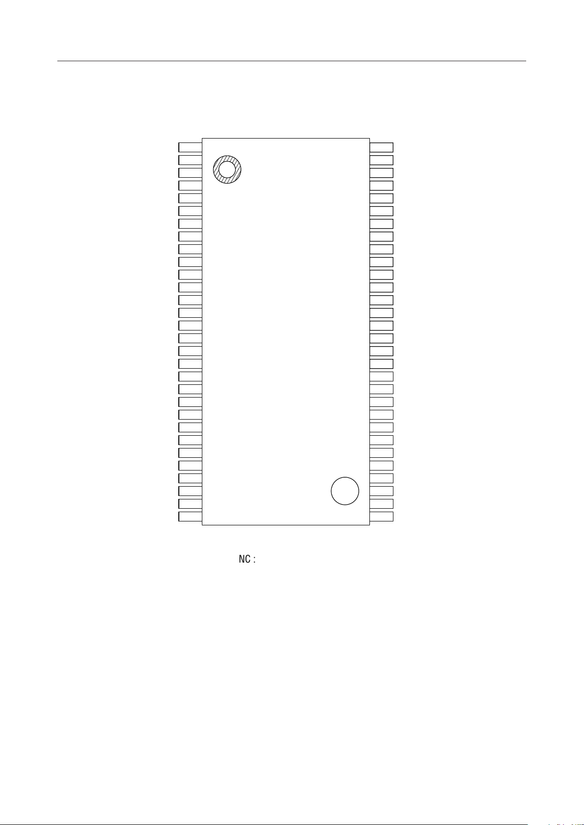
PIN CONFIGURATION (TOP VIEW)
HVO 1
HVO 2
HVO 3
HVO 4
HVO 5
HVO 6
HVO 7
HVO 8
HVO 9
HVO 10
HVO 11
HVO 12
HVO 13
HVO 14
HVO 15
HVO 16
HVO 17
HVO 18
HVO 19
HVO 20
V
HV
GND 1
GND 2
CL
NC
LS
NC
R/L
DIN
V
CC
10
11
12
13
14
15
16
17
18
19
20
21
22
23
24
25
26
27
28
29
30
1
2
3
4
5
6
7
8
9
60
59
58
57
56
55
54
53
52
51
50
49
48
47
46
45
44
43
42
41
40
39
38
37
36
35
34
33
32
31
HVO 40
HVO 39
HVO 38
HVO 37
HVO 36
HVO 35
HVO 34
HVO 33
HVO 32
HVO 31
HVO 30
HVO 29
HVO 28
HVO 27
HVO 26
HVO 25
HVO 24
HVO 23
HVO 22
HVO 21
V
HV
GND 1
GND 2
NC
CHG
NC
CLK
NC
DOUT
V
CC
NC : No-connection pin
60-Pin Plastic SSOP
5/14
Page 6
¡ Semiconductor MSC1162A
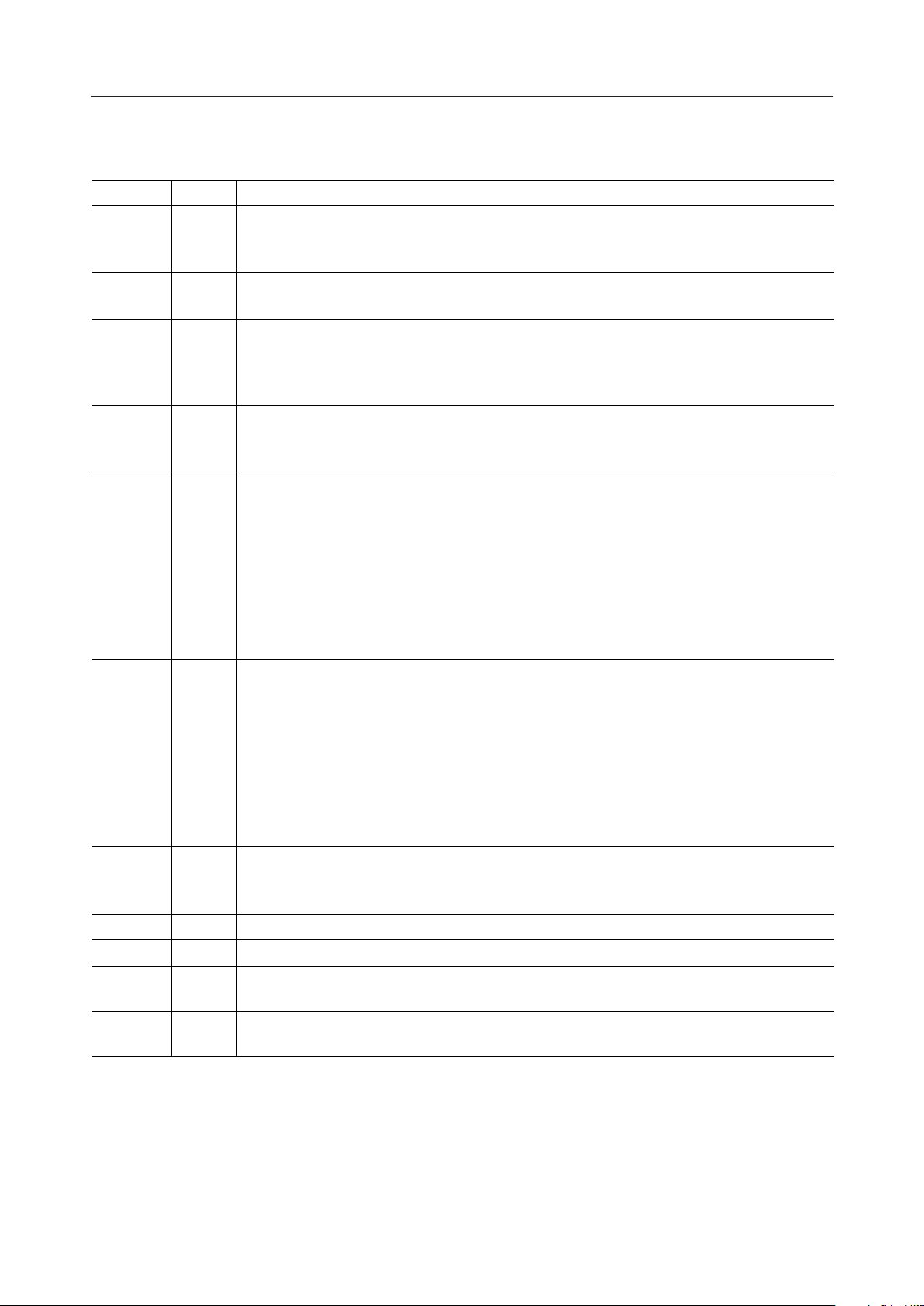
PIN DESCRIPTION
Symbol Description
CLK
DIN
DOUT
LS
CL
Type
I
I
O
I
I
Shift register clock input pin.
Shift register reads data through DIN while the CLK pin is low state and the data in the shift
register is shifted from one stage to the next stage at the rising edge of the clock.
Serial data input pin of the shift register.
Display data (positive logic) is input in through the DIN pin synchronization with clock.
Serial data output pin of the shift register.
Data is output through the DOUT pin in synchronization with the CLK signal.
When R/L = High, the data of PO40 in the shift register is output through the DOUT pin.
When R/L = Low, the data of PO1 pin in the shift register is output through the DOUT pin.
Latch strobe input pin
When LS is high, the parallel output data (PO1-40) of the shift register read out. When LS
goes from high to low, the parallel output data (PO1-40) of the shift register is held.
Clear input pin with a built-in pull-up resistor
The CL pin is normally being set high.
If the CL pin is high and the CHG pin is low, the driver outputs (HV01 to HV40) are in phase
with the corresponding latch outputs (O1 to O40).
If the CL pin is high and the CHG pin is high, the driver outputs (HV01 to HV40) are high
irrespective of the states of the latch outputs.
If the CL pin is set low, the driver outputs are driven low irrespective of the states of the
CHG pin and latch outputs.
This allows display blanking to be set.
CHG
VHO1-40
VHV
VCC
GND1
GND2
Input for testing (with a pull-down resistor)
The CL pin is normally being set low.
If the CHG pin is low and the CL pin is high, the driver outputs (HV01 to HV40) are in phase
with the corresponding latch outputs (O1 to O40).
I
If the CHG pin is low and the CL pin is low, the driver outputs (HV01 to HV40) are low
irrespective of the states of the latch outputs.
If the CHG pin is set high, the driver outputs are driven high irrespective of the states of the
latch outputs.
This provides the easy testing of all lights after final assembly.
High voltage driver outputs for driving VFD tube
O
The driver outputs are in phase with the corresponding latch outputs (O1 to O40).
The direct connection to the grid or anode of a VFD tube eliminates pull-down resistors.
Power supply pin for driver circuits of VFD tube
Power supply pin for logic
GND pin for driver circuits of a VFD tube. (D-GND)
Since the GND1 is not be connected to L-GND, connect this pin to the external L-GND.
GND pin for the logic circuits. (L-GND)
Since the GND2 pin is not be connected to D-GND, connect this pin to the external D-GND.
6/14
Page 7
¡ Semiconductor MSC1162A
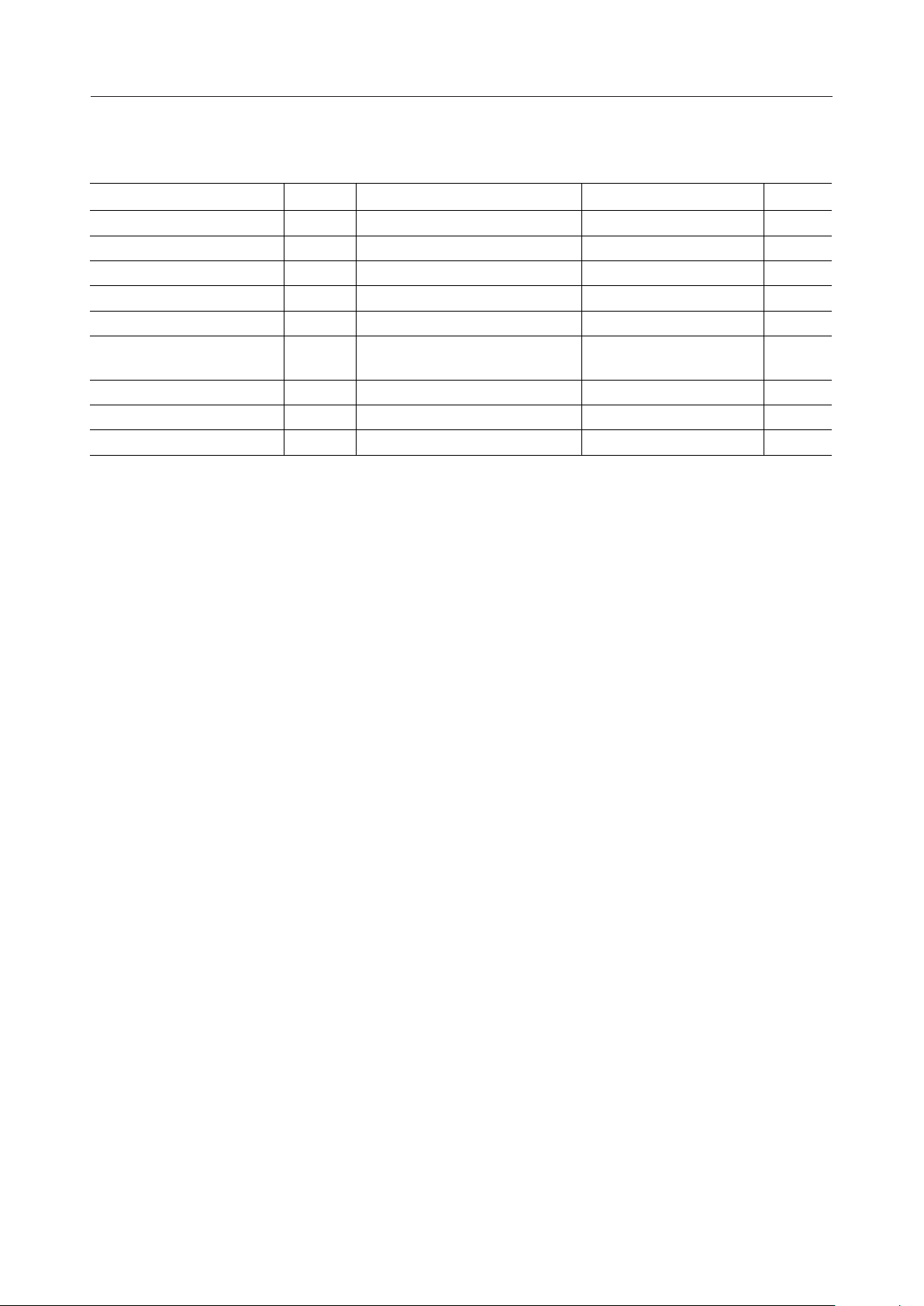
ABSOLUTE MAXIMUM RATINGS
Parameter Symbol Condition Rating Unit
Logic Supply Voltage V
Driver Supply Voltage V
Input Voltage V
Output Voltage V
*1
*1, *2
*1
*1
Driver Driving Frequency f
Withstand Output Voltage
*1, *2
V
Power Dissipation P
Package Thermal Resistance
*3
Storage Temperature T
DRV
HVO
R
STG
CC
HV
IN
O
D
j-a
Applicable to logic supply pin
Applicable to driver supply pin
Applicable to all input pins
Applicable to data output pin
–0.3 to +6.5 V
–0.3 to +70 V
–0.3 to VCC +0.3 V
–0.3 to VCC +0.3 V
0 to 15 kHzApplicable to driver output pin
–0.3 to VHV +0.3 VApplicable to driver output pin
860
145 °C/WTa > 25°C
–55 to +150 °C—
Notes: *1 Maximum Supply Voltage with respect to L-GND and D-GND
*2 Permanent damage may be caused if the voltage is supplied over the rating value.
*3 Package Thermal Resistance (between junction and ambient)
The junction temperature (Tj) expressed by the equation indicated below should not
exceed 150°C.
Tj=P ¥ R
+Ta (P: Maximum power consumption)
j–a
mWTa £ 25°C
7/14
Page 8
¡ Semiconductor MSC1162A
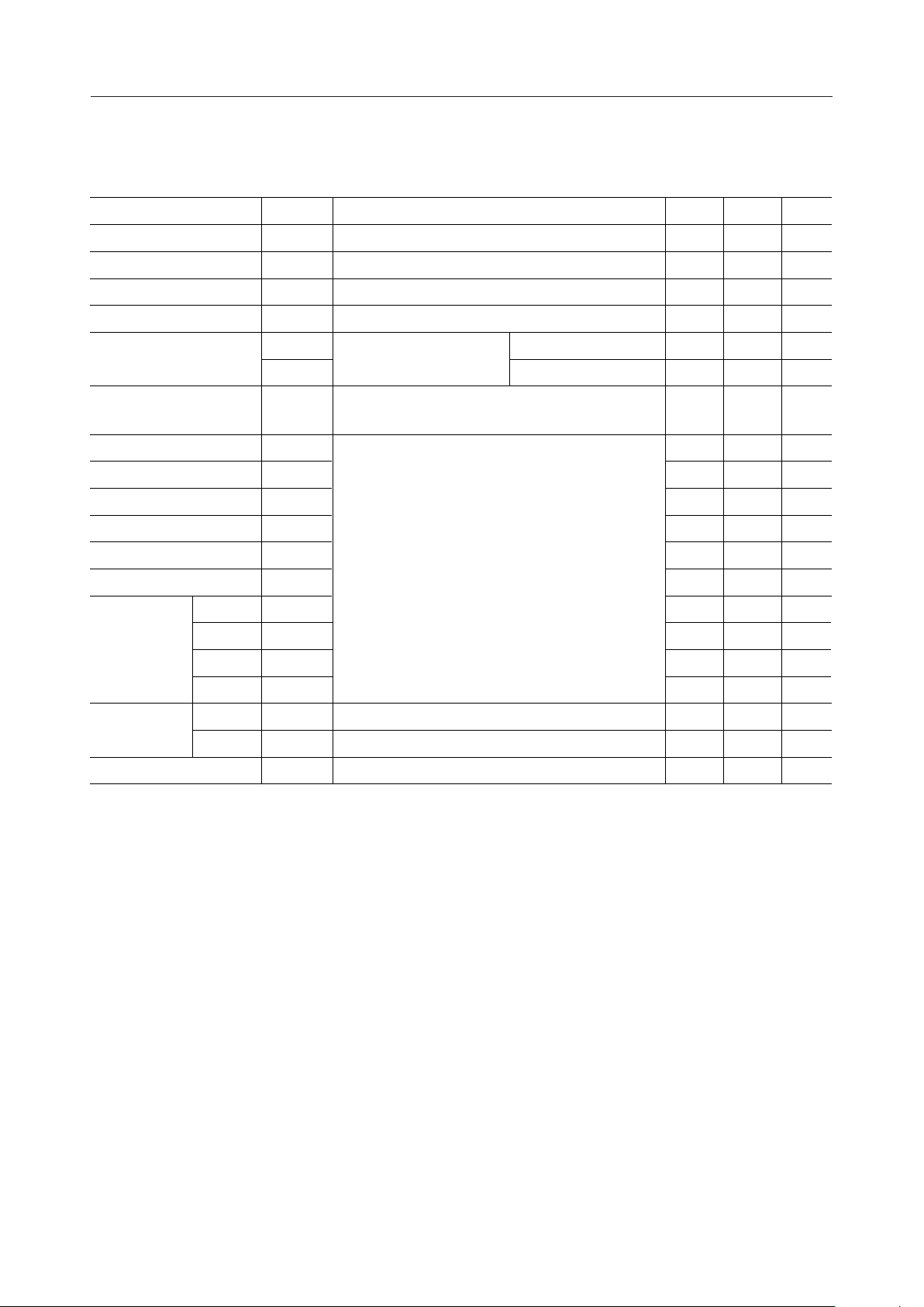
RECOMMENDED OPERATING CONDITIONS
Parameter Symbol Condition Max. Unit
Logic Supply Voltage V
High Level Input Voltage V
Low Level Input Voltage V
High Level Driver Output
Current
I
OHVH1
I
OHVH2
Low Level Driver Output
Current
CLK Frequency f
CLK Pulse Width tw
Data Setup Time t
Data Hold Time th
SU
(CLK-D)
Data Pulse Width tw
Latch Probe Pulse Width tw
CLK-LS tsu
LS-CLK tsu
Setup Time
LS-CHG tsu
(CLK-LS)
(LS-CLK)
(LS-CHG)
LS-CL tsu
CHG
tw
Pulse Width
CL
tw
Operating Temperature T
CC
HV
IH
IL
OHVL
CLK
(CLK)
(D-CLK)
(D)
(LS)
(LS-CL)
(CHG)
(CL)
op
Applicable to logic supply voltage pin
Applicable to driver supply voltage pinDriver Supply Voltage V
Applicable to all input pins
Applicable to all input pins
Applicable to driver
output pin
Only one output is high
All outputs are high
Applicable to all driver output pinsI
See timing diagram
—
—
—
Min.
4.5
140
80
5.5 V
65 V10
—V3.6
1.1 V—
–40 mA—
–2 mA—
1mA—
4 MHz—
—ns75
—ns80
—ns50
—ns
—ns
—ns50
—ns0
— ms0
— ms0
— ms2
— ms2
85 °C–40
8/14
Page 9
¡ Semiconductor MSC1162A
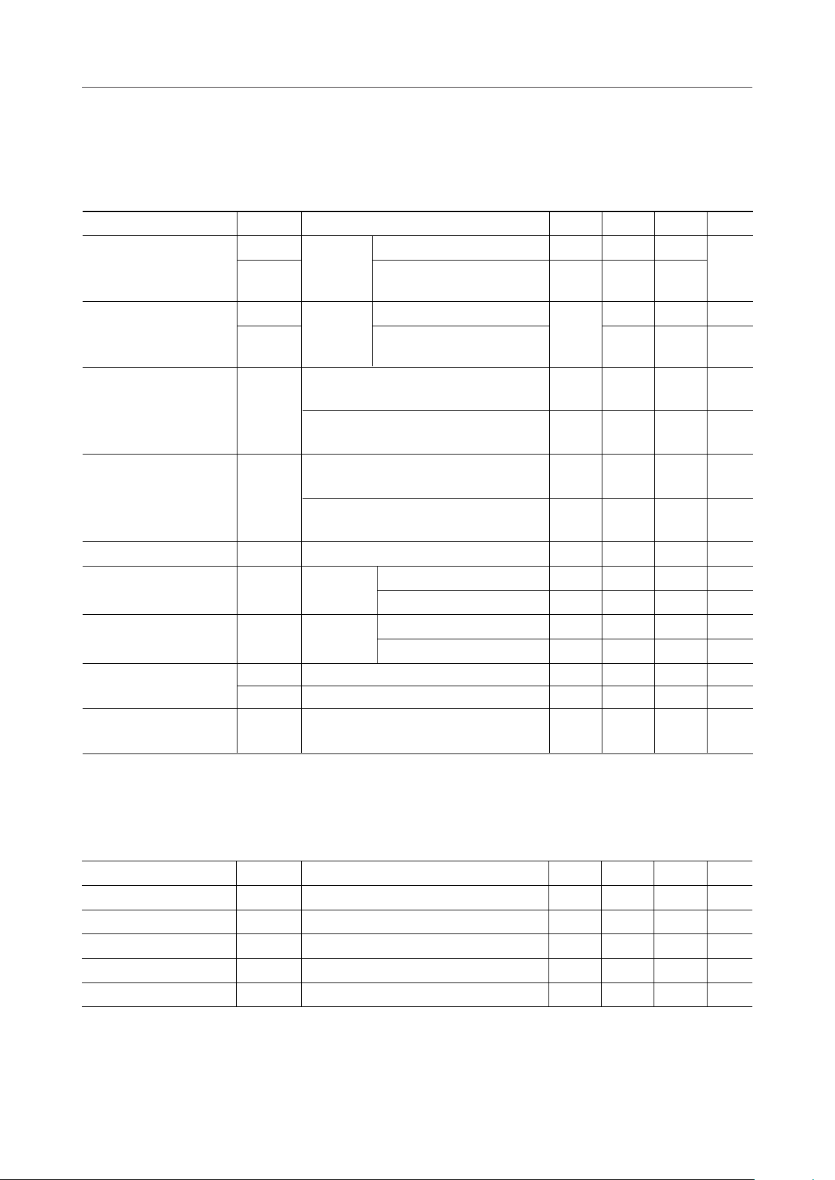
ELECTRICAL CHARACTERISTICS
DC Characteristics
(V
=4.5 to 5.5V, VHV=10 to 65V, Ta=–40 to +85°C)
CC
Parameter Symbol Condition Max. Unit
Min.
Typ.
Logic Supply Current
Driver Supply Current
High Level Input Current
Low Level Input Current
High Level Data Output
Voltage
Low Level Data Output
Voltage
High Level Driver Output
Voltage
Low Level Driver Output
Voltage
I
I
I
HV1
I
HV2
V
V
V
OHVH1
V
OHVH2
OHVL
CC1
CC2
I
IH
I
IL
I
ODH
ODL
No load
V
=5.5V
CC
No load
V
=5.5V
CC
IOH=–0.1mA
I
=0.1mA
OL
All input: Low
All input: High,
Ta=25°C
All input: Low
All input: High
Ta=25°C
V
=5.5V, VIN=5.5V
CC
Inputs excluding CHG
VCC=5.5V, VIN=5.5V
CHG input
VCC=5.5V, VIN=0V
Inputs excluding CL
VCC=5.5V, VIN=0V
CL input
Ta=25°CInput Capacitance C
VCC=4.5V ——3.5
V
=5.5V ——4.5
CC
VCC=4.5V 1.1——
V
=5.5V 1.1——
CC
IOH=–40mA
IOH=–2mA
IOL=1mAV
HV
—
—
–4
4.3
—
6.65
1.00.5—
1.0
3.82.45
1—–1
80—5
1—–1
–80—–5
—pF15—
—V—VHV–4
—V—V
3.0 V——
mA
mA
mA
mA
mA
mA
mA
V
V
V
V
AC Characteristics
Parameter Symbol Condition Max. UnitTyp.Min.
CLK-DOUT Delay Time t
Delay Time Low to High t
Transit Time Low to High t
Delay Time High to Low t
Transit Time High to Low t
PD
DLH
TLH
DHL
THL
—
—
—
—
—
(V
=5V, VHV=65V, Ta=25°C)
CC
300 ns——
1.0 ms0.3—
5.0 ms2.0—
1.0 ms0.3—
5.0 ms2.0—
9/14
Page 10
¡ Semiconductor MSC1162A
10/14
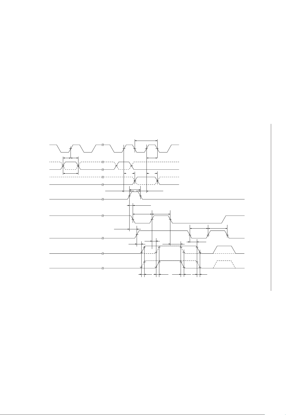
TIMING DIAGRAM
1/f
CLK
CLK
DIN
LS
HVO (OTHERS)
CL
HVO (1, 2, 39, 40)
CHG
DOUT
T1/2 T3/4
T39/40
T1/2 T3/4
tw
(CLK)
th
(CLK-D)
tsu
(D-CLK)
tw
(D)
t
PD
t
PD
tsu
(CLK-LS)
tw
(LS)
tsu
(LS-CHG)
tsu
(LS-CL)
tw
(CL)
tw
(CL)
t
DLH
t
DLH
t
TLH
tsu
(LS-CLK)
tw
(CHG)
tw
(CHG)
t
DHL
t
DHL
t
TLH
t
THL
t
THL
Page 11
¡ Semiconductor MSC1162A
FUNCTIONAL DESCRIPTION
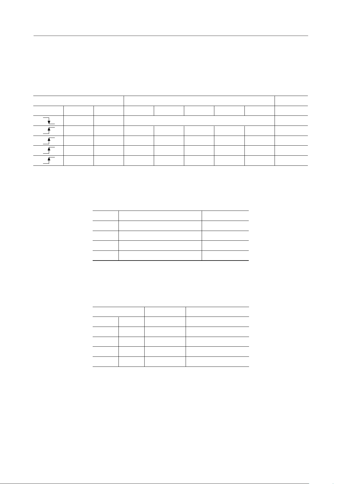
Function Table
Shift register
Input Shift Register Parallel Out Output
CLK R/L DIN PO1 PO39PO2 PO40 DOUT
X X Not changed
H L L PO38nPO1n PO39n PO40
H H H PO38nPO1n PO39n PO40
L L PO2n PO40nPO3n L PO1
L H PO2n PO40nPO3n H PO1
X: Don't Care
PO1n to PO40n : PO1 to PO40 data just before CLOCK rises.
Latch
Input Shift Register Parallel Out Latch Output
LS POm Om
I X Not changed
HL L
HH H
X: Don't Care, m: 1 to 40
Not changed
Driver output
Input Driver Output
CL Om HVOm
LXL
HXH
HLL
HHH
X: Don't Care, m: 1 to 40
CHG
Latch Output
X
H
L
L
11/14
Page 12

¡ Semiconductor MSC1162A
NOTES ON USE
1. Connect GND1 to GND2 externally to be an equal potential voltage.
2. The contents of the shift register are undefined when the power is applied.
Therefore, unnecessary driver outputs may be driven high just after power-on, and
the VFD tube may flicker.
To avoid this, follow the procedures:
1) Apply the driver power supply after applying the logic power supply, with the
CL pin remained low.
2) Start displaying by setting the CL pin high after in putting display data the shift
register through the DIN pin.
12/14
Page 13
¡ Semiconductor MSC1162A
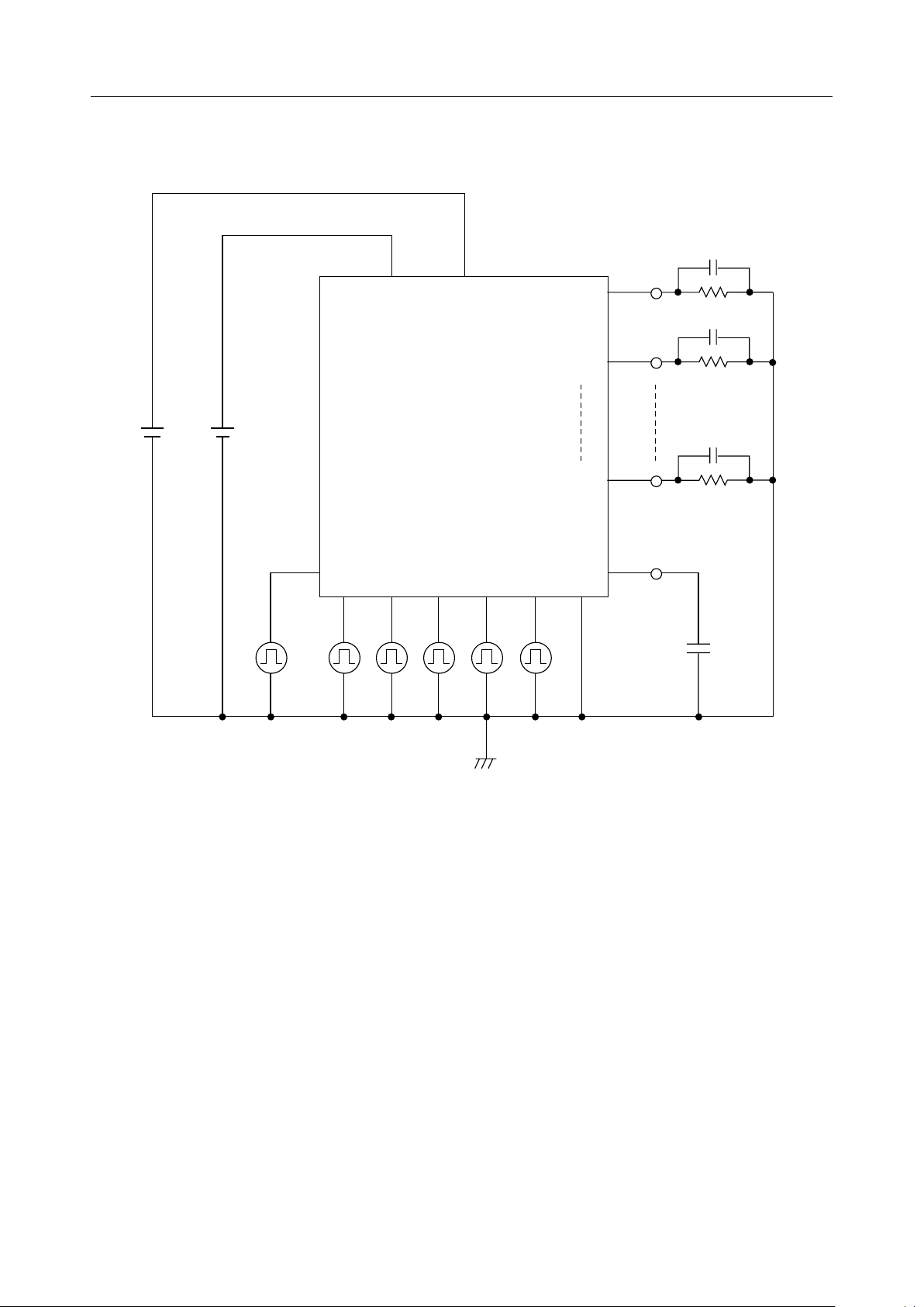
Test circuit
20pF
65V 5.0V
DIN
CLK
V
CC
V
HV
HVO1
1.5kW
HVO2
HVO40
DOUT
LS
R/L
CHG
CL
GND1, 2
30pF
13/14
Page 14
¡ Semiconductor MSC1162A
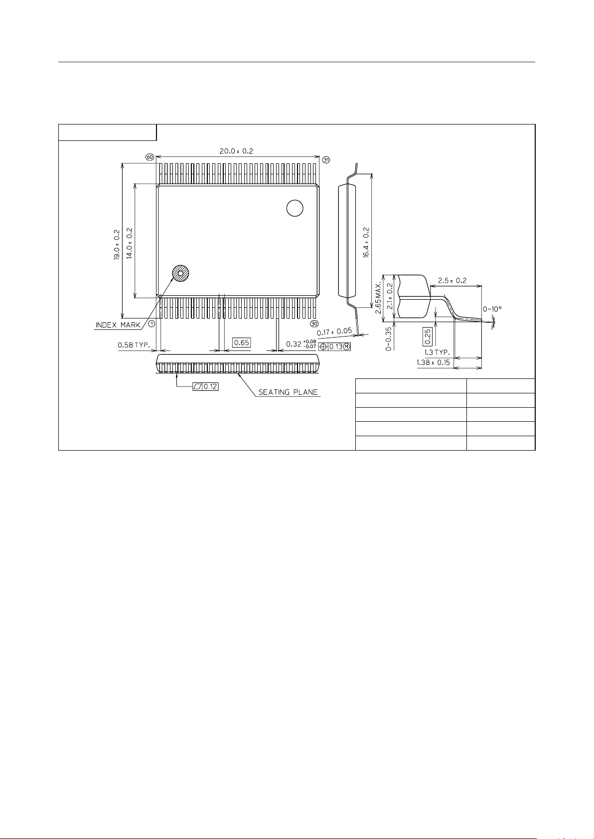
PACKAGE DIMENSIONS
(Unit : mm)
SSOP60-P-700-0.65-BK
Mirror finish
Package material
Lead frame material
Pin treatment
Solder plate thickness
Package weight (g)
Epoxy resin
42 alloy
Solder plating
5 mm or more
1.21 TYP.
Notes for Mounting the Surface Mount Type Package
The SOP, QFP, TSOP, SOJ, QFJ (PLCC), SHP and BGA are surface mount type packages, which
are very susceptible to heat in reflow mounting and humidity absorbed in storage.
Therefore, before you perform reflow mounting, contact Oki’s responsible sales person for the
product name, package name, pin number, package code and desired mounting conditions
(reflow method, temperature and times).
14/14
 Loading...