

M48T86
5V PC REAL TIME CLOCK
■ DROP-IN REPLACEMENT for PC
COMPUTER CLOCK/CALENDAR
■ COUNTS SECONDS, MINUTES, HOURS,
DAYS, DAY of the WEEK, DATE, MONTH and
YEAR with LEAP YEAR COMPENSATION
■ INTERFACED WITH SOFTWARE AS 128
RAM LOCATIONS:
– 14 Bytes of Clock and Control Registers
– 114 Bytes of General Purpose RAM
■ SELECTABLE BUS TIMING (Intel/Motorola)
■ THREE INTERRUPTS are SEPARATELY
SOFTWARE-MASKABLE and TESTABLE
– Time-of-Day Alarm (Once/Second to
Once/Day)
– Periodic Rates from 122µs to 500ms
– End-of-Clock Update Cycle
■ PROGRAMMABLE SQUARE WAVE OUTPUT
■ SELF-CONTAINED BATTERY and CRYSTAL
in the CAPHAT DIP PACKAGE
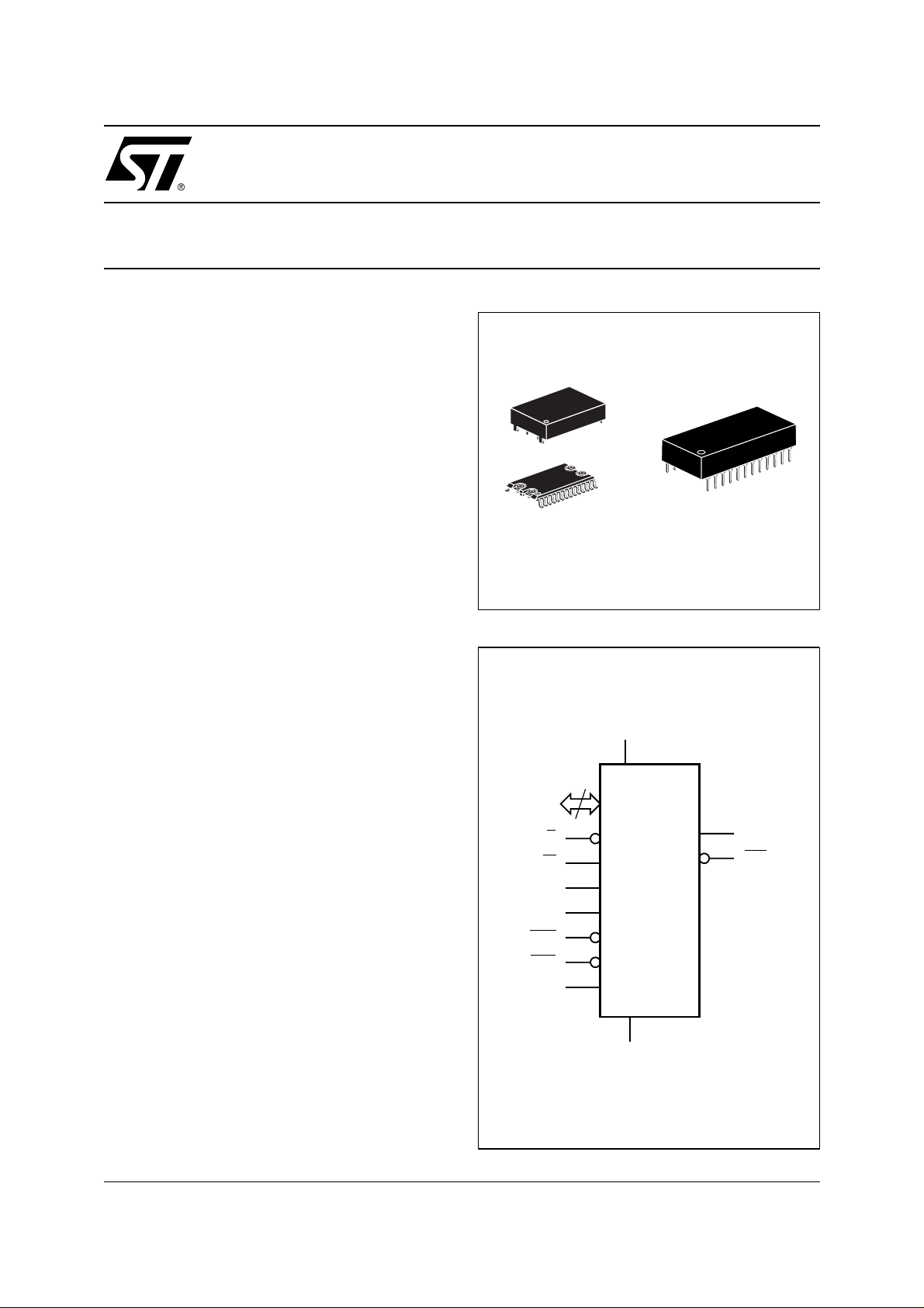
■ PACKAGING INCL UD ES a 28- L EAD SOIC
and SNAPHAT
®
TOP
(to be Ordered Separately)
■ SOIC PACKAGE PROVIDES D IREC T
CONNECTION for a SNAPHAT TOP
CONTAINS the BATTERY and CRYSTAL
■ PIN and FUNCTION COMPATIBLE with
bq3285/7A and DS128887
SNAPHAT (SH)
Battery/Crystal
28
1
SOH28 (MH)
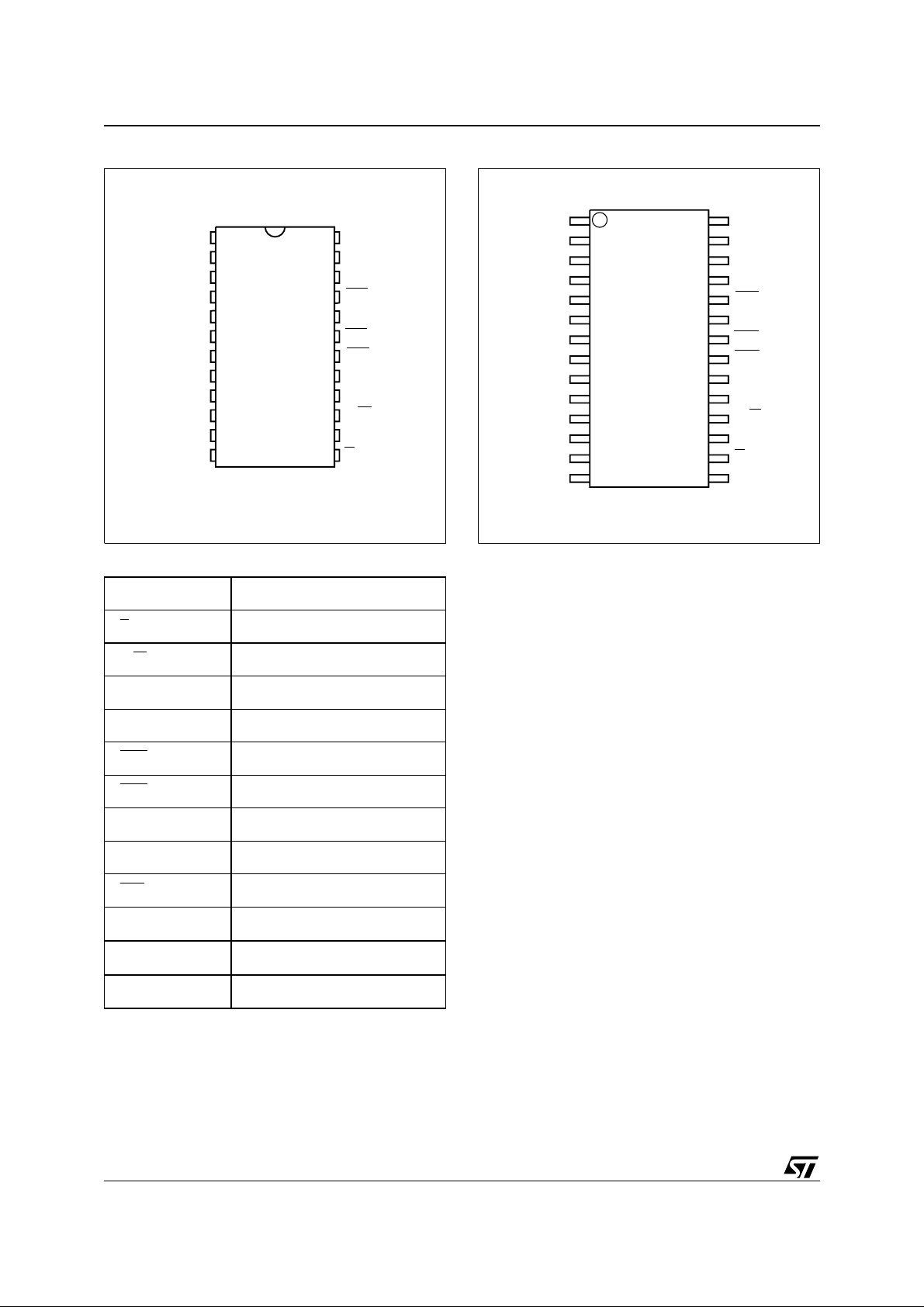
Figure 1. Logic Diagram
V
CC
8
AD0-AD7
E
R/W
DS
AS
RST
RCL
MOT
M48T86
24
1
PCDIP24 (PC)
Battery/Crystal
CAPHAT
SQW
IRQ
V
SS
AI01640
1/23May 2000
M48T86
Figure 2. DIP C on ne ctions
MOT V
1
2
NC
3
NC
4
AD0
5
AD1
6
AD2
AD3
AD4
AD5
AD6
V
SS
M48T86
7
8
9
10
11
12 13
24
23
22
21
20
19
18
17
16
15
14
AI01641
CC
SQW
NC
RCL
NC
IRQ
RST
DS
NC
R/W
ASAD7
E
Table 1. Signal Names
AD0-AD7 Multiplexed Address/Data Bus
E
R/W
DS Data Strobe Input
AS Add ress Strob e Input
RST
RCL
MOT Bus Type Select Input
SQW Square Wave Output
IRQ
V
CC
V
SS
NC Not Connected Internally
Chip Enable Input
Write Enable Input
Reset Input
RAM Clear Input
Interrupt Request Output
Supply Voltage
Ground
Figure 3. SOIC Connections
1
MOT V
NC
NC
AD0
AD1
AD2
AD3
AD4
AD5
AD6
V
SS
V
SS
2
3
4
5
6
7
8
9
10
11
12
13
14
M48T86
28
27
26
25
24
23
22
21
20
19
18
17
16
15
AI01642
NCNC
CC
SQW
NC
RCL
NC
IRQ
RST
DS
NC
R/W
ASAD7
E
NC
DESCRIPTION
The M48T86 is an industry standard real time
clock (RTC).The M48T86 is composed of a lithium
energy source, quartz crystal, write-protection c ircuitry, and a 128 byte RAM array. This prov ides
the user with a complete subsystem packaged in
either a 24-pin DIP CAPHAT or 28-pin SNA PH AT
SOIC. Functions available to the user include a
non-volatile time-of-day clock, alarm interrupts, a
one-hundred-year clock with programmable in terrupts, square wave output, and 128 bytes of nonvolatile stat ic R AM .
The 24 pin 600mil DIP CAPHAT™ houses the
M48T86 silicon with a quartz crystal and a long life
lithium button cell in a single package.
The 28 pin 330mil SOIC provides sockets with
gold plated contacts at both ends for direct connection to a separate SNAPHAT housing cont aining the battery and crystal. The unique design
allows the SNAPHAT battery package to be
mounted on top of the SOIC package after the
completion of the surface mount process.
Insertion of the SNAPHAT housing after reflow
prevents potential battery and crystal damage due
to the high temperatures required for device surface-mounting. The SNAPHAT housing is keyed
to prevent reverse insertion.
The SOIC and battery packages are shipped separately in plastic anti-static tubes or in Tape & Reel
form.
2/23

M48T86
Table 2. Absolute Maximum Ratings
Symbol Parameter Value Unit
T
A
T
STG
(2)
T
SLD
V
IO
V
CC
P
D
Note: 1. Stresses greater than those listed under "Absolute Maximum Ratings" may cause permanent damage to the device. This is a stress
rating only and functional operation of the devi ce at these or any other condi t i ons above those indicated in the operational section
of this spec ification is not im plied. Exposure t o the abso lute max imum rat ing cond itions for extende d period s of tim e may affe ct
reliability.
2. Soldering temperature not to exceed 260°C for 10 seconds (total thermal budget not to exceed 150°C for longer than 30 seconds).
CAUTION: Negative undershoots below –0.3V are not allowed on any pin whil e i n the Batter y Back-up mode.
CAUTION: Do NOT wave solder SOIC to avoid damaging SNAPHAT sockets.
Ambient Operating Temperature 0 to 70 °C
Storage Temperature (VCC Off, Oscillator Off)
Lead Solder Temperature for 10 seconds 260 °C
Input or Output Voltages –0.3 to 7.0 V
Supply Voltage –0.3 to 7.0 V
Power Dissipation 1 W
For the 28 lead SOIC, the battery/crystal package
part number is "M4T28-BR12SH1".
Automatic deselection of the device provides insurance that data integrity is not compromised
should V
lect Voltage (V
fall below specified Power-fail Dese-
CC
) levels. The automatic deselec-
PFD
tion of the device remains in effect upon power up
for a period of 200ms (max) after V
V
, provided that the Real Time Clock is running
PFD
and the count down chain is not reset. This allows
sufficient time for V
to stabilize and gives the
CC
system clock a wa ke up p er i o d so th a t a valid system reset can be established.
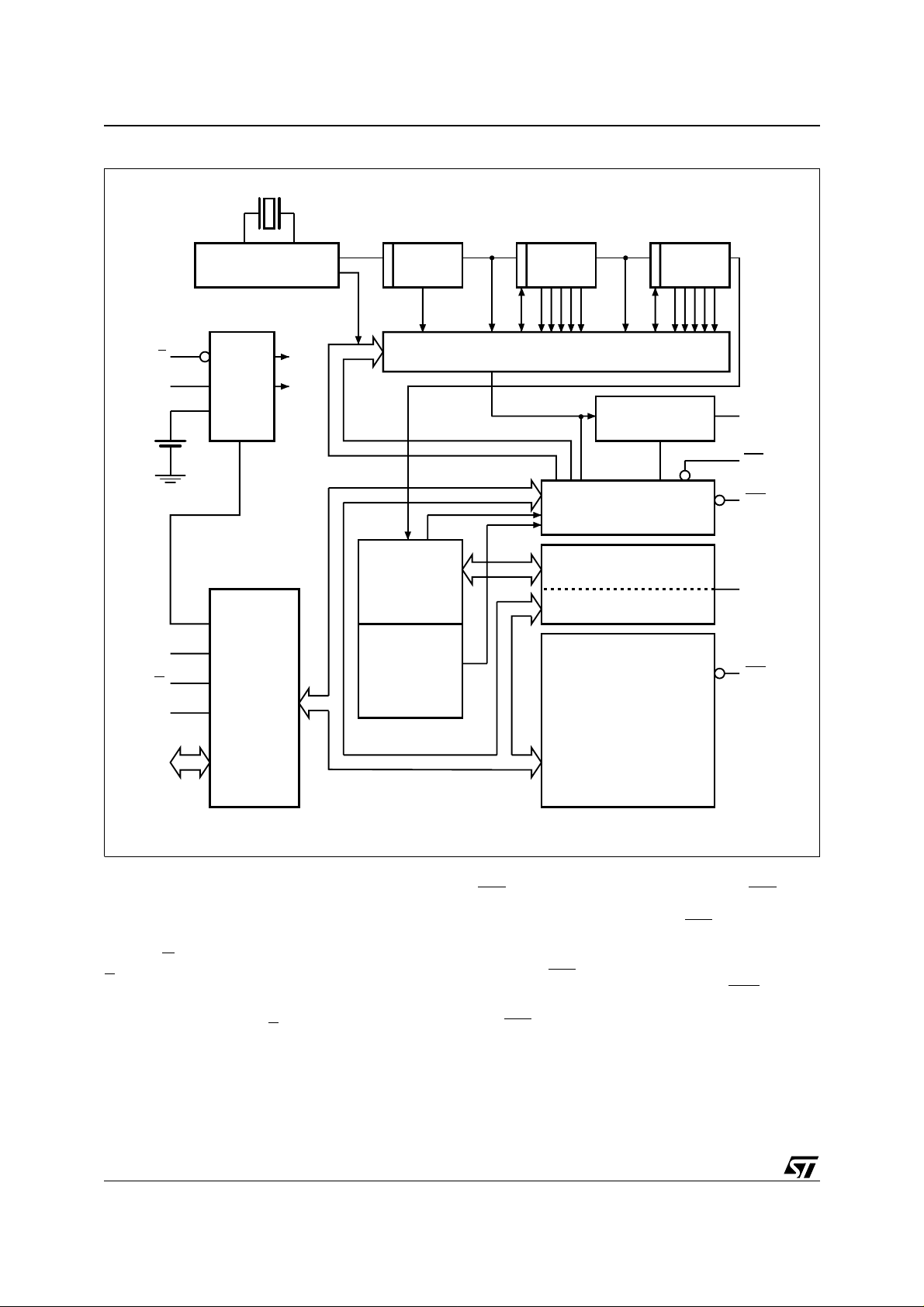
The block diagram in F igure 3 shows the pi n c onnections and the major internal functions of the
M48T86.
SIGNAL DESCRIPTION
V
, VSS. DC power is provided to the device on
CC
these pins.The M48T86 utilizes a 5V V
SQW (Square Wave Output). During n ormal op-
eration (i.e. valid V
), the SQW pin can output a
CC
signal from one of 13 taps.The frequenc y of the
SQW pin can be changed by programming Register A as shown in T able 10. Th e SQW signal can
be turned on and off using the SQWE bit (Register
B; bit 3). The SQW signal is not available when
V
is less than V
CC
PFD
.
(1)
rises above
CC
.
CC
–40 to 85 °C
AD0-AD7 (Multiplexed Bi-Directional Address/
Data Bus). The M48T86 provides a multiplexed
bus in which address an d data information s hare
the same signal path. The bus cycle consists of
two stages; first the address is latched, followed by
the data. Address/Data multiplexing does not slow
the access time of the M48T86, since the bus
change from address to data occurs during the internal RAM access time. Addresse s must be valid
prior to the falling edge of AS, at which time the
M48T86 latches the address present on AD0AD7. Valid write data must be present and held
stable during the latter port ion of the R/W
pulse. In
a read cycle, the M48T86 outputs 8 bits of data
during the latter portion of the DS pulse. The read
cycle is terminated and the bus returns to a high
impedance state upon a high transition on R/W
.
AS (Address Strobe Input). A positive going
pulse on the Address Strobe (AS) inp ut serves to
demultiplex the bus. The falling edge of AS causes
the address present on AD0-AD7 to be latched
within the M48T86.
MOT (Mode Select). The MOT pin offers the flexibility to choose between two bus types. When
connected to V
When connected to V
, Motorola bus timing is selected.
CC
or left disconnected, Intel
SS
bus timing is selected. The pin has an internal pulldown resistance of approximately 20K ohms.
3/23
M48T86
Figure 4. Block Diagram
V
V
BAT
R/W
CC
DS
AS
OSCILLATOR
E
POWER
SWITCH
AND
WRITE
PROTECT
BUS
INTERFACE
V
CC
POK
/ 8 / 64 / 64
PERIODIC INTERRUPT/SQUARE WAVE SELECTOR
REGISTERS A,B,C,D
CLOCK/
CALENDAR
UPDATE
BCD/BINARY
INCREMENT
CLOCK CALENDAR,
AND ALARM RAM
STORAGE
REGISTERS
(114 BYTES)
SQUARE WAVE
OUTPUT
SQW
IRQ
RST
DOUBLE
BUFFERED
RCL
AD0-AD7
DS (Data Strobe Input). The DS pin is also referred to as Read (RD). A falling edge transition on
the Data Strobe (DS) input enables the output during a a read cycle. This is very similar to an Output
Enable (G
(Chip Enable Input). The Chip Enable pin
E
) signal on other memory devices.
must be asserted low for a bus cycle in the
M48T86 to be accessed. Bus cycles which take
place without asserting E
will latch the addresses
present, but no data access will occur.
4/23
AI01643
IRQ (Inte rr upt R eq ue st Ou t put) . The IRQ pin is
an open drain output that can be used as an interrupt input to a processor. The IRQ
output remains
low as long as the status bi t causing the interrupt
is present and t he corresponding interrup t-enable
bit is set. IRQ
whenever Register C is read. The RST
returns to a hi gh impedance state
pin can
also be used to clear pending interrupts. Because
the IRQ
external pul l-up resis tor to V
bus is an open drain output, it requires an
.
CC

M48T86
RST (Reset Input). The M48T86 is reset when
the R ST
plied and a low on RST
input is p ulled lo w. With a valid VCC ap-
, the following event s oc-
cur:
1. Periodic Interrupt Enable (PIE) bit is cleared to
a zero. (Register B; Bit 6)
2. Alarm Interrupt Enable (AIE) b it is cleared to a
zero.(Register B; bit 5)
3. Update Ended Interrupt Request (UF) bit is
cleared to a zero. (Register C; Bit 4)
4. Interrupt Request (IRQF) bit is cleared to a zero.
(Register C Bit 7)
5. Periodic Interrupt Flag (PF) bit is cleared to a
zero. (Register C; Bit 6)
6. The device is not accessible until RST
is re-
turned high.
7. Alarm Interrupt Flag (AF) bit is cleared to a zero.
(Register C; Bit 5)
8. The IRQ
pin is in the high impedance state.
9. Square Wave Output Enable (SQWE) bit is
cleared to zero. (Register B; Bit 3).
10.Update Ended Interrupt Enable (UIE) is cleared
to a zero. (Register B; Bit 4)
RCL
(RAM Clear). The RCL pin is used to clear
all 114 storage bytes, excluding clock and control
registers, of the array to FF(hex ) value. T he array
will be cleared when the RCL
pin is held low for at
least 100ms with the osc illator running. Usage of
this pin does not affect battery load. This function
is applicable only when V
(Read/Write Input). The R/W pin i s utilized
R/W
is applied .
CC
to latch data into the M 48T86 and prov ides functionality si milar to W
in other memory systems.
ADDRESS MAP
The address map of the M48T86 is shown in Figure 9. It consists of 114 bytes of user RAM, 10
bytes of RAM that contain the RTC time, calendar
and alarm data, and 4 bytes which are used for
control and status. All bytes can be read or written
to except for the following:
1. Registers C & D are read-only.
2. Bit 7 of Register A is read-only.
The contents of the four Registers A, B, C, and D
are described in the "Registers" section.
5/23
M48T86
Table 3. Time, Calendar and Alarm Formats
Address RTC Bytes
Decimal Binary BCD
0 Seconds 0-59 00-3B 00-59
1 Seconds Alarm 0-59 00-3B 00-59
2 Minutes 0-59 00-3B 00-59
3 Minutes Alarm 0-59 00-3B 00-59
Hours, 12-hrs 1-12
4
Hours, 24-hrs 0-23 00- 17 00-23
Hours Alarm, 12-hrs 1-12
5
Hours Alarm, 24-hrs 0-23 00-17 00-23
6 Day of Week (1 = Sun) 1-7 01-07 01-07
7 Day of Month 1-31 01-1F 01-31
8 Month 1-12 01-0C 01-12
9 Year 0-99 00-63 00-99
Range
01-0C AM
81-8C PM
01-0C AM
81-8C PM
01-12 AM
81-92 PM
01-12 AM
81-92 PM
TIME, CALENDAR, AND ALARM LOCATIONS
The time and calendar information is obtained by
reading the appropriate memory bytes. Th e time,
calendar, and alarm registers are set o r initialized
by writing the appropriate RAM bytes. The contents of the time, calendar, and alarm bytes can be
either Binary or Binary-Coded Decimal (BCD) format. Before writing the internal time, calendar, and
alarm register, the SET bit (Register B; Bit 7)
should be written to a logic "1". This will prev ent
updates from occurring while access is being attempted. In addition to writing the time, calendar,
and alarm registers in a selected format (binary or
BCD), the Data Mode (DM) bit (Register B ; Bit 2),
must be set to the appropriate logic level ("1" signifies binary data; "0" signifies Binary Coded Decimal (BCD data). All time, calendar, and alarm
bytes must use the same data mode. The SET bit
should be cleared after the Data Mode bit has
been written to allow the Real Time Clock to update the time and calendar bytes. Once initialized,
the Real Time Clock makes all updates in the selected mode. The da ta mode cann ot be changed
without reinitializing the ten data bytes. Table 3
shows the binary and BCD formats of the time, calendar, and alarm loc ations. The 24/ 12 bit (Register B; Bit 1) cannot be changed without
reinitializing the hour locations. When the 12-hour
format is selected, a logic one in the high order bit
of the hours byte represents PM. The time, calendar, and alarm bytes are always accessible because they are double buffered. Once per second
the ten bytes are advanced by one second and
checked for an alarm condition. If a read of the
time and calendar data occurs during an update, a
problem exists where seconds, minutes, hours,
etc. may not correlate. However, the probability of
reading incorrect time and calendar data is low.
Methods of avoiding possible incorrect time and
calendar reads are reviewed later in this text.
NON-VOLATILE RAM
The 114 general purpose non-volatile RAM bytes
are not dedicated to any special function within the
M48T86. They can be used by t he proces sor program as non-volatile me mory a nd a re f ully a ccessible during the update cycle.
6/23
M48T86
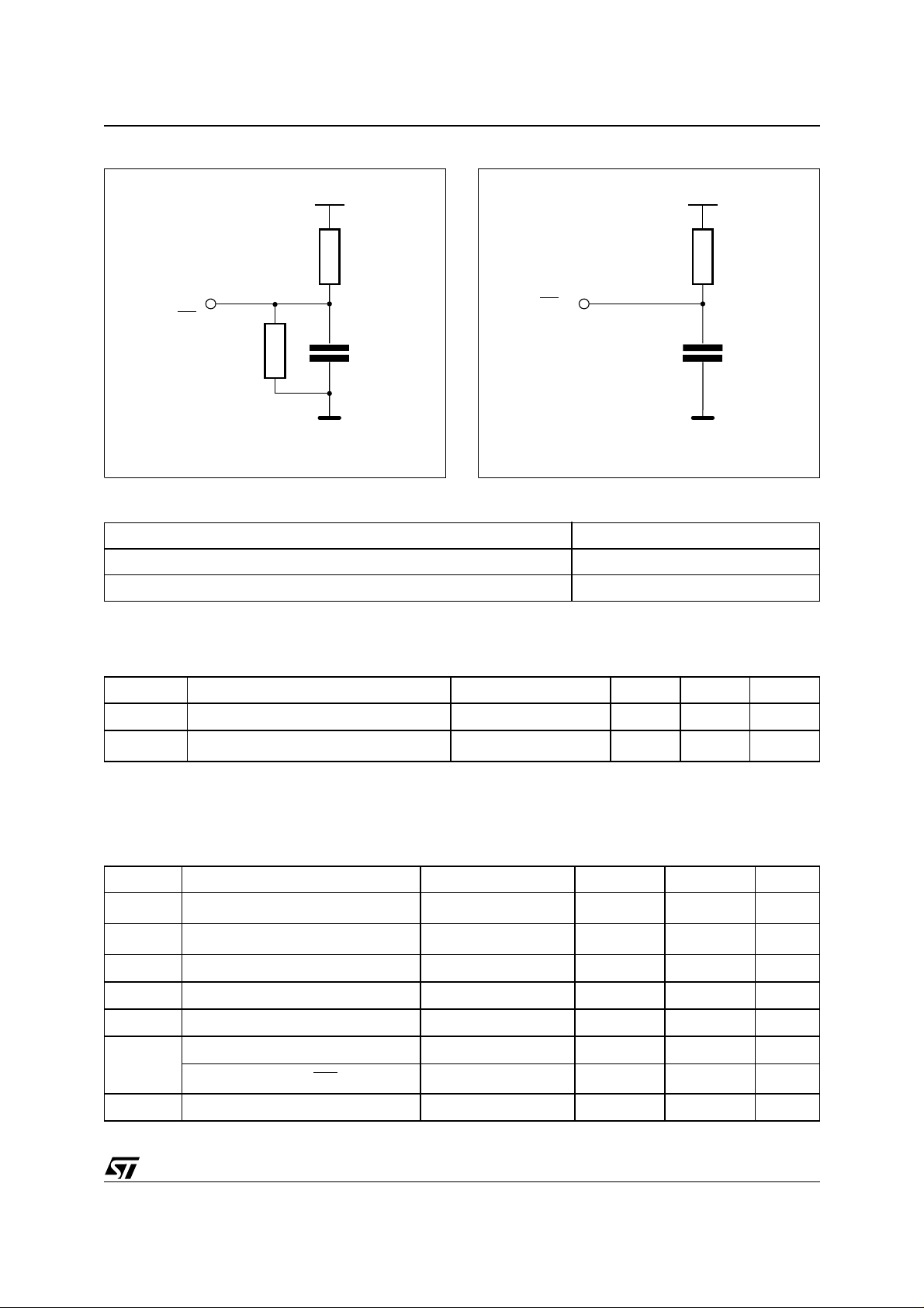
Figure 5. AC Testing Load Circuit
5V
FOR ALL
OUTPUTS
EXCEPT IRQ
510Ω
960Ω
50pF
AI01644
Figure 6. AC Testing Load Circuit
IRQ
Table 4. AC Measurement Conditions
Input Rise and Fall Times ≤ 5ns
Input Pulse Voltages 0 to 3V
Input and Output Timing Ref. Voltages 1.5V
Note that Output Hi-Z is defined as the point where data is no longer driven.
5V
1.15kΩ
130pF
AI01645
Table 5. Capacitance
= 25 °C, f = 1 MHz)
(T
A
(1, 2)
Symbol Parameter Test Condition Min Max Unit
V
V
OUT
IN
= 0V
= 0V
7pF
5pF
C
IN
C
IO
Note: 1. Effective capacitance measured with power supply at 5V .
2. Sampled only, not 100% tested.
3. Outputs desele ct ed.
Input Capacitance
(3)
Input / Output Capacitance
Table 6. DC Characteristics (1)
= 0 to 70 °C; VCC = 4.5V to 5.5V)
(T
A
Symbol Parameter Test Condition Min Max Unit
(1)
Input Leakage Current
I
LI
(1)
I
LO
I
CC
V
V
Output Leakage Current
Supply Current Outputs open 15 mA
Input Low Voltage –0.3 0.8 V
IL
Input High Voltage 2.2
IH
Output Low Voltage
V
OL
Output Low Voltage (IRQ
V
OH
Note: 1. Outputs deselected .
Output High Voltage
)
0V ≤ V
0V ≤ V
I
OL
I
OL
I
OH
≤ V
IN
≤ V
OUT
= 4mA
= 0.5mA
= –1mA
CC
CC
±1 µA
±1 µA
V
+ 0.3
CC
0.4 V
0.4 V
2.4 V
V
7/23
 Loading...