

M48T59
M48T59Y/M48T59V
64 Kbit (8Kb x8) TIMEKEEPER® SRAM
PRELIMINARY DATA
■ INTEGRATED ULTRA LOW POWER SRAM,
REAL TIME CLOCK, POWER-FAIL CONTROL
CIRCUIT and BATTERY
■ FREQUENCY TEST OUTPUT for REAL TIME
CLOCK SOFTWARE CALIBRATION
■ AUTOMATIC POWER-FAIL CHIP DESELECT
and WRITE PROTECTION
■ WRITE PROTECT VOLTAGES
(V
= Power-fail Deselect Voltage):
PFD
– M48T59: 4.5V ≤ V
– M48T59Y: 4.2V ≤ V
– M48T59V: 2.7V ≤ V
■ SELF-CONTAINED BATTERY and CRYSTA L
PFD
PFD
PFD
≤ 4.75V
≤ 4.5V
≤ 3.0V
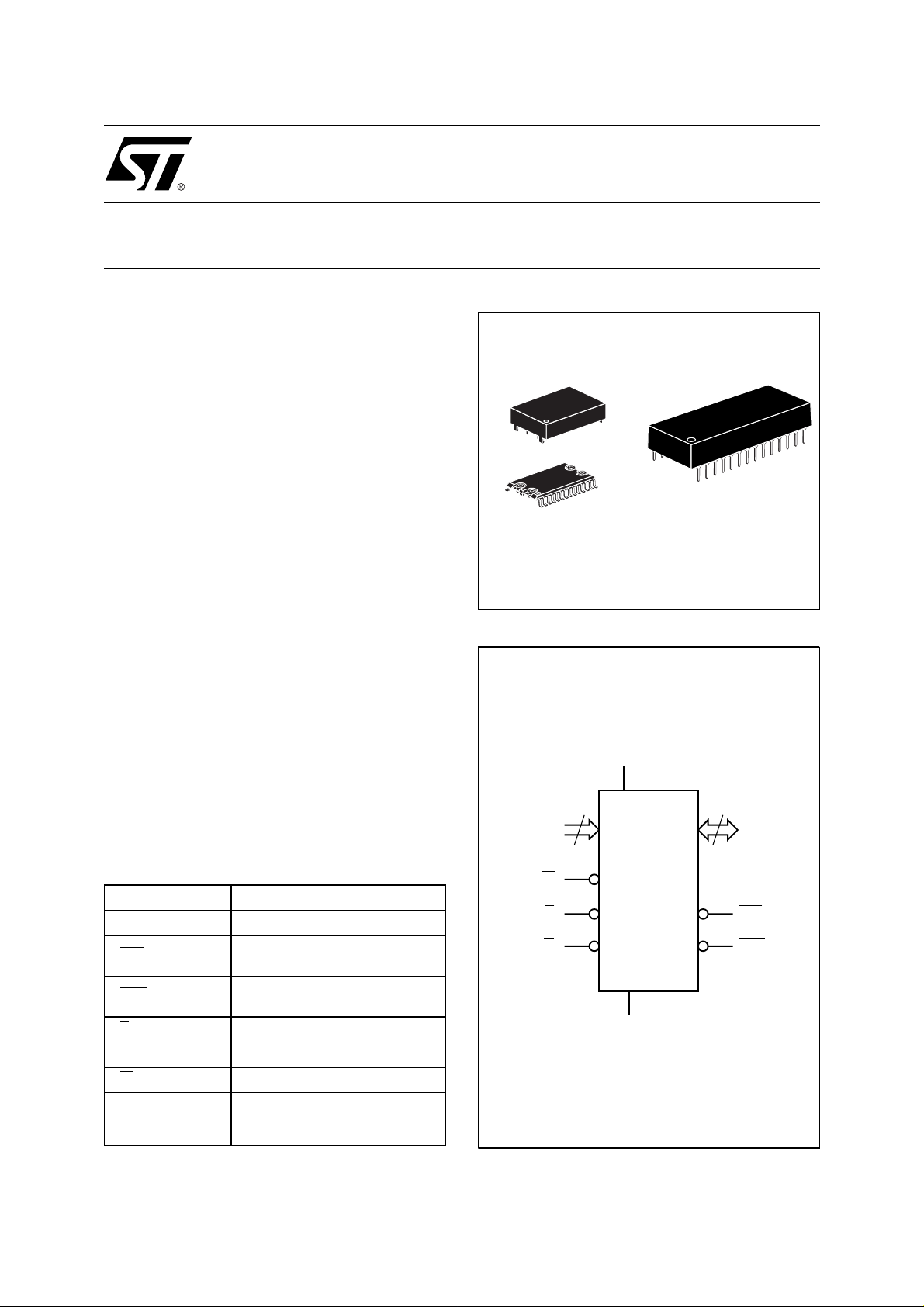
in the CAPHAT DIP PACKAGE
■ PACKAGING INCLUDES a 28-LEAD SOIC and
SNAPHAT
®
TOP
(to be Ordered Separately)
■ SOIC PACKAGE PROVIDES D IREC T
CONNECTION for a SNAPHAT TOP which
CONTAINS the BATTERY and CRYSTAL
■ MICROPROCESSOR POWER-ON RESET
(Valid even during battery back-up mode)
■ PROGRAMM ABLE A L A R M O U TPUT ACTIVE
in the BATTERY BACK-UP MODE
■ BATTERY LOW FLAG
SNAPHAT (SH)
Battery/Crytstal
28
28
1
SOH28 (MH)
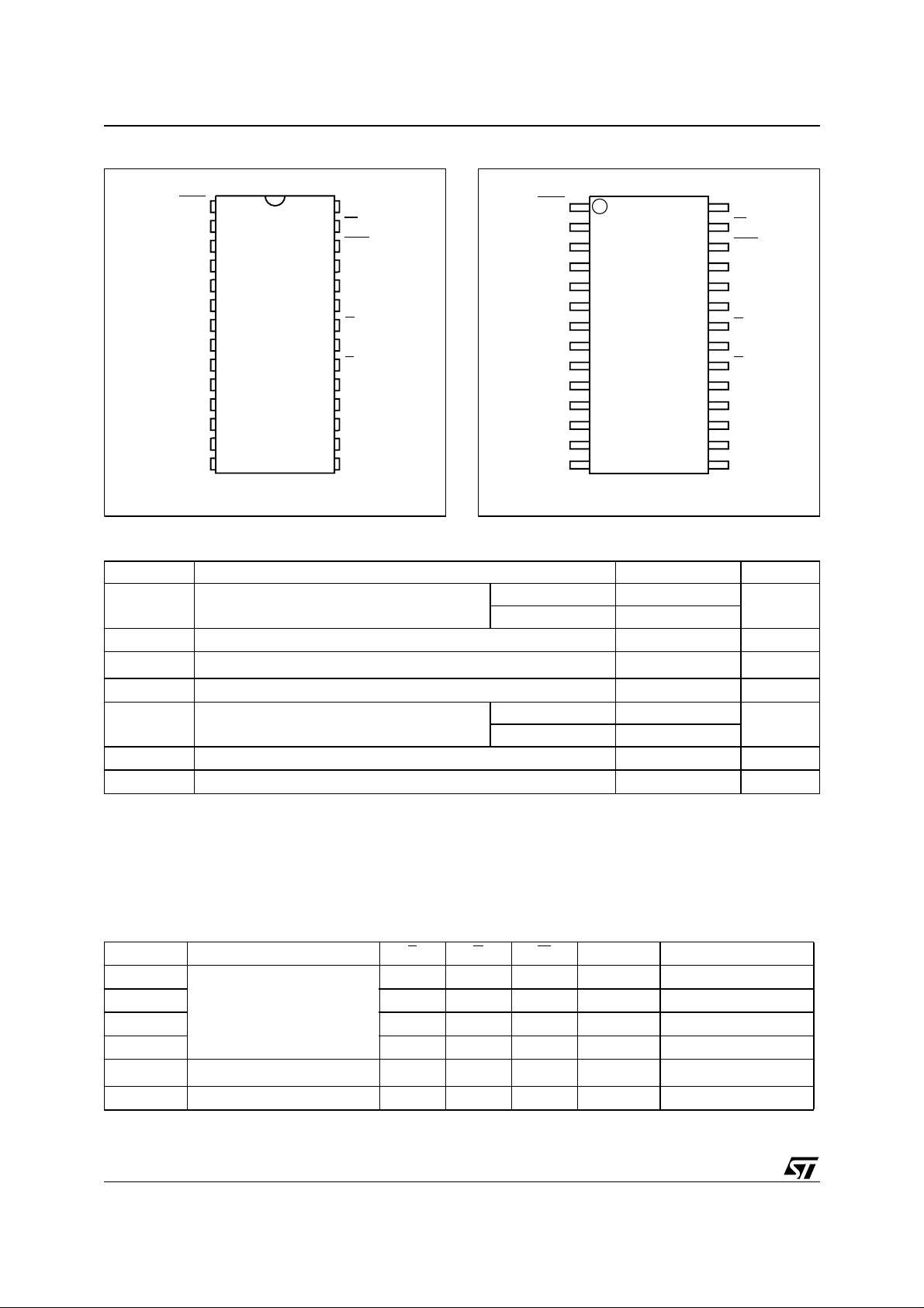
Figure 1. Logic Diagram
V
CC
13
A0-A12
1
PCDIP28 (PC)
Battery/Crystal
CAPHAT
8
DQ0-DQ7
Table 1. Signal Names
A0-A12 Address Inputs
DQ0-DQ7 Data Inputs / Outputs
IRQ
/FT
RST
E
G
W
V
CC
V
SS
October 1999
This is preliminary information on a new product now in development or undergoing evaluation. Details are subject to change without notice.
Interrupt / Frequency Test
Output (Open Drain)
Power Fail Reset Output
(Open Drain)
Chip Enable
Output Enable
Write Enable
Supply Voltage
Ground
W
E
G
M48T59
M48T59Y
M48T59V
V
SS
IRQ/FT
RST
AI01380E
1/21
M48T59, M48T59Y, M48T59V
Figure 2A. DIP Connections
RST V
1
A12
2
3
A7
4
A6
5
A5
6
A4
7
A3
A2
A1
A0
DQ0
8
9
10
11
M48T59
M48T59Y
12
13
DQ2
14
SS
28
27
26
25
24
23
22
21
20
19
18
17
16
15
AI01381D
CC
W
IRQ/FT
A8
A9
A11
G
A10
E
DQ7
DQ6
DQ5DQ1
DQ4
DQ3V
Table 2. Absolute Maximum Ratings
(1)
Figure 2B. SOIC Connections
RST V
A12
A7
A6
A5
A4
A3
A2
A1
A0
DQ0
DQ2
SS
1
2
3
4
5
6
7
M48T59Y
8
M48T59V
9
10
11
12
13
14
AI01382E
28
27
26
25
24
23
22
21
20
19
18
17
16
15
CC
W
IRQ/FT
A8
A9
A11
G
A10
E
DQ7
DQ6
DQ5DQ1
DQ4
DQ3V
Symbol Parameter Value Unit
T
A
T
STG
T
SLD
V
IO
V
CC
I
O
P
D
Note: 1. Stresses greater than those listed under "Absolute Maximum Ratings" may cause permanent damage to the device. This is a stress
2. Soldering temperature not to exceed 260°C for 10 seconds (total thermal budget not to exceed 150°C for longer than 30 seconds).
CAUTION: Negative undershoots below –0.3V are not allowe d on any pin while i n the Batter y Back-up mod e.
CAUTION: Do NOT wave solder SOIC to avoid damaging SNAPHAT sockets.
Ambient Operating Temperature
Storage Temperature (VCC Off, Oscillator Off)
(2)
Lead Solder Temperature for 10 seconds 260 °C
Input or Output Voltages –0.3 to 7 V
Supply Voltage
Output Current 20 mA
Power Dissipation 1 W
rating only and functional opera tion of the devi ce at these or any other conditions above those i ndi cated in th e operational section
of this spec ification is not im plied. Exposure t o the abso lute max imum rat ing cond itions for extende d period s of tim e may affe ct
reliability.
Grade 1 0 to 70
Grade 6 –40 to 85
–40 to 85 °C
M48T59/M48T59Y –0.3 to 7
M48T59V –0.3 to 4.6
°C
V
V
PFD
≤ V
CC
or
or
SO
(1)
(min)
(2)
E G W DQ7-DQ0 Power
V
IH
V
IL
V
IL
V
IL
X X X High Z CMOS Standby
X X X High Z Battery Back-up Mode
Table 3. Operating Modes
Mode
Deselect
Write
Read
Read
Deselect
Deselect
Note: 1. X = VIH or VIL; VSO = Battery Back-up Swit ch ov er Volta ge.
2. See T able 7 for deta ils.
4.75V to 5.5V
4.5V to 5.5V
3.0V to 3.6V
V
to V
SO
2/21
X X High Z Standby
X
V
IL
V
IH
V
IL
V
IH
V
IH
D
D
OUT
IN
Active
Active
High Z Active
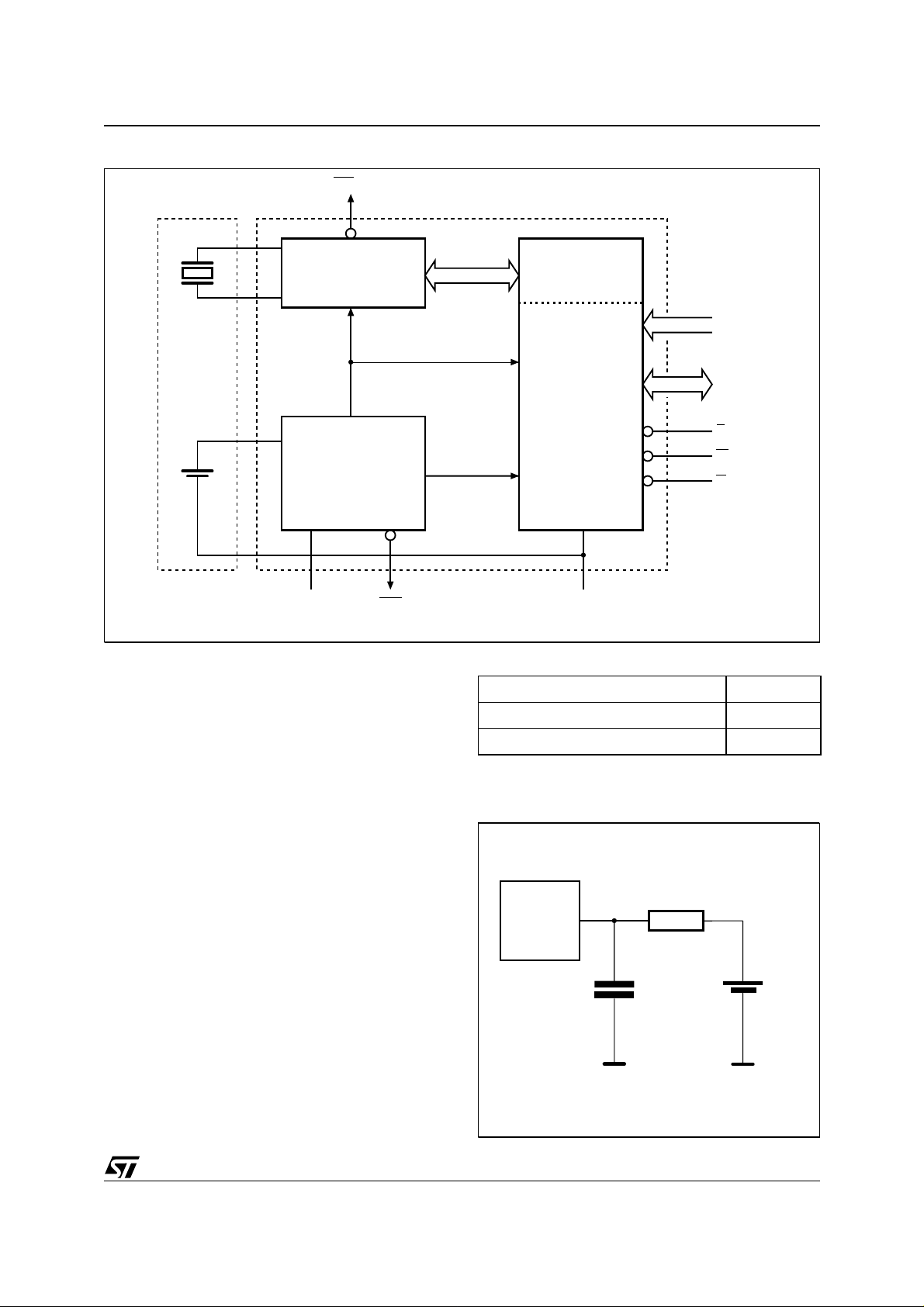
Figure 3. Block Diagram
M48T59, M48T59Y, M48T59V
IRQ/FT
OSCILLATOR AND
CLOCK CHAIN
32,768 Hz
CRYSTAL
POWER
LITHIUM
CELL
VOLTAGE SENSE
AND
SWITCHING
CIRCUITRY
CC
RSTV
DESCRIPTION
®
The M48T59/59Y/59V TIMEKEEPER
RAM is an
8Kb x8 non-volatile static RAM and real time clock.
The monolithic chip is available in two special
packages to provide a highly integrated battery
backed-up memory and real time clock solution.
The M48T59/59Y/59V is a non-volatile pin and
function equivalent to any JEDEC standard 8Kb x8
SRAM. It also easily fits into many ROM, EPROM,
and EEPROM sockets, providing the non-volatility
of PROMs without any requirement for special
write timing or limitations on the number o f writes
that can be performed.
The 28 pin 600mil DIP CAPHAT™ houses the
M48T59/ 5 9Y /59V silic o n with a quartz c ry st al and
a long life lithium button cell in a single package.
The 28 pin 330mil SOIC provides sockets with
gold plated contacts at both ends for direct connection to a separate SNAPHAT housing cont aining the battery and crystal. The unique design
allows the SNAPHAT battery package to be
mounted on top of the SOIC package after the
completion of the surface mount process. Insertion of the SNAPHAT housing after reflow prevents potential battery and c rystal dam age due to
the high temperatures required for device surfacemounting. The SNAPHAT housing is keyed to prevent reverse insertion.
16 x 8 BiPORT
SRAM ARRAY
A0-A12
DQ0-DQ7
E
W
G
AI01383D
V
PFD
8176 x 8
SRAM ARRAY
V
SS
Table 4. AC Measurement Conditions
Input Rise and Fall Times ≤ 5ns
Input Pulse Voltages 0 to 3V
Input and Output Timing Ref. Voltages 1.5V
Note that Output Hi-Z is defined as the point where data is no longer
driven.
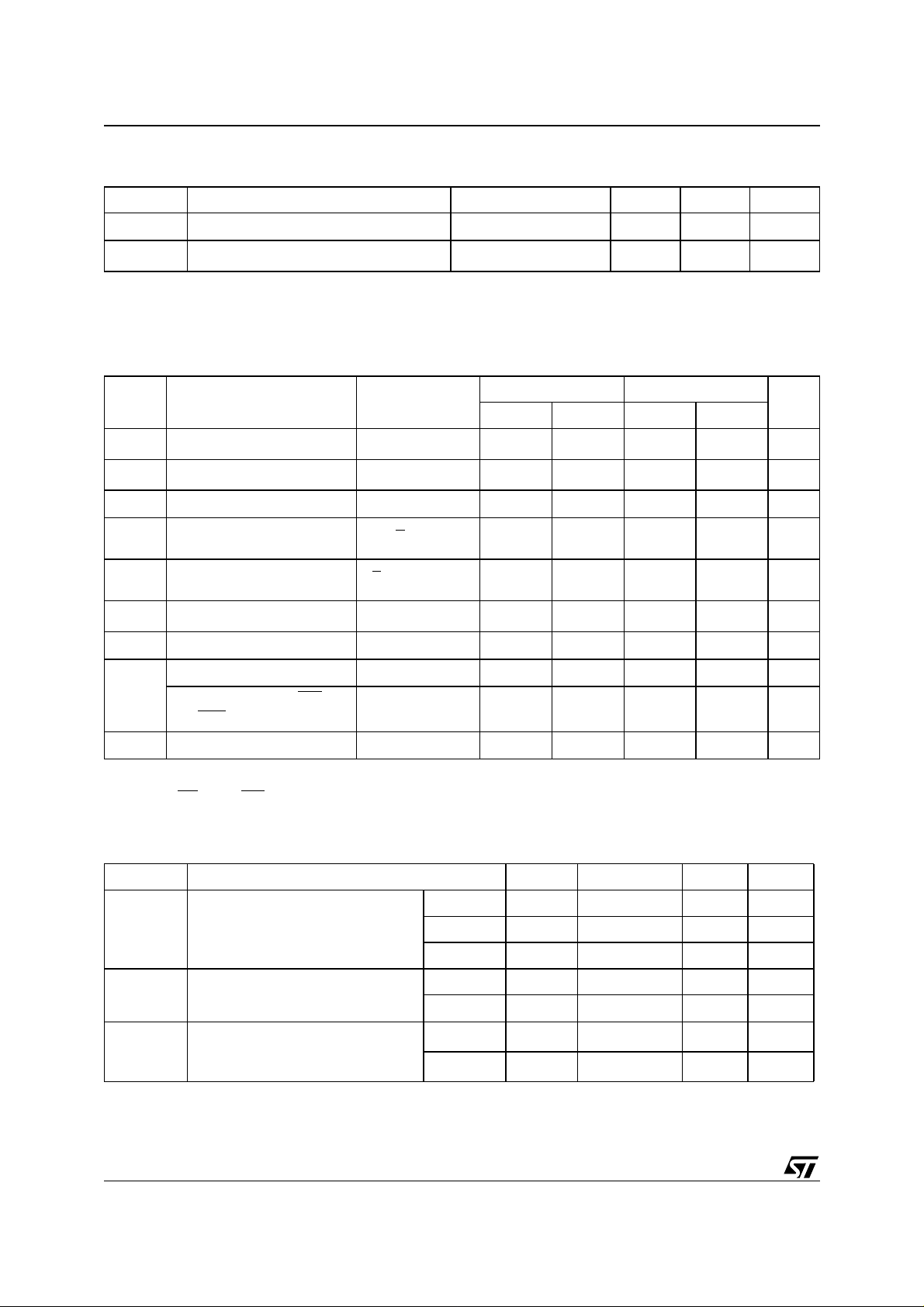
Figure 4. AC Testing Load Circuit
DEVICE
UNDER
TEST
CL includes JIG capacitance
Note: Excluding open-drain output pins.
645Ω
CL = 100pF
AI02325
1.75V
3/21
M48T59, M48T59Y, M48T59V
Table 5. Capacitance
(T
= 25 °C)
A
(1, 2)
Symbol Parameter Test Condition Min Max Unit
C
C
IO
Note: 1. Effective capacitance measured with power suppl y at 5V.
2. Sampled only, not 100% tested.
3. Outputs desele ct ed.
Input Capacitance
IN
(3)
Input / Output Capacitance
V
V
OUT
IN
= 0V
= 0V
10 pF
10 pF
Table 6. DC Characteristics
(T
= 0 to 70 °C or –40 to 85 °C; VCC = 4.75V to 5.5V or 4.5V to 5.5V or 3.0V to 3.6V)
A
Symbol Parameter Test Condition
(1)
I
LI
I
LO
I
I
I
V
V
Input Leakage Current
(1)
Output Leakage Current
Supply Current Outputs open 50 30 mA
CC
Supply Current (Standby)
CC1
TTL
Supply Current (Standby)
CC2
CMOS
(2)
Input Low Voltage –0.3 0.8 –0.3 0.8 V
IL
Input High Voltage 2.2
IH
Output Low Voltage
V
OL
Output Low Voltage (IRQ
(3)
and RST
V
Note: 1. Outputs deselected.
Output High Voltage
OH
2. Negativ e s p i k e s of –1V allo wed for up to 10ns onc e pe r cycle .
3. The I RQ
)
/FT and RS T pi ns are Open Drain.
/FT
0V ≤ V
IN
0V ≤ V
OUT
= V
E
= VCC – 0.2V
E
I
= 2.1mA
OL
IOL = 10mA
I
= –1mA
OH
≤ V
≤ V
IH
CC
CC
M48T59/Y M48T59V
Min Max Min Max
±1 ±1 µA
±1 ±1 µA
32mA
31mA
V
CC
+ 0.3
2
VCC + 0.3
0.4 0.4 V
0.4 0.4 V
2.4 2.4 V
Unit
V
Table 7. Power Down/Up Trip Points DC Characteristics
(1)
(TA = 0 to 70 °C or –40 to 85 °C)
Symbol Parameter Min Typ Max Unit
M48T59 4.5 4.6 4.75 V
V
PFD
V
SO
t
DR
Note: 1. All voltages referenced to VSS.
2. Usi ng larger M4T 32-BR12SH6 SNAPHA T top (recomm ended for I ndustrial Te m perature Range - grade 6 device).
4/21
Power-fail Deselect Voltage
Battery Back-up Switchover Voltage
Expected Data Retention Time (at 25 °C)
M48T59Y 4.2 4.35 4.5 V
M48T59V 2.7 2.9 3.0 V
M48T59/Y 3.0 V
V
M48T59V
Grade 1
Grade 6
10
7
(2)
PFD
–100mV
V
YEARS
YEARS
M48T59, M48T59Y, M48T59V
Table 8. Power Down/Up AC Characteristics
(T
= 0 to 70 °C or –40 to 85 °C)
A
Symbol Parameter Min Max Unit
t
PD
(1)
t
F
t
FB
t
R
t
RB
t
REC
Note: 1. V
2. V
3. t
E or W at VIH before Power Down
V
(max) to V
PFD
(2)
V
(min) to VSS VCC Fall Time
PFD
V
(min) to V
PFD
VSS to V
(3)
V
(max) to V
PFD
(min).
es V
PFD
(min) to VSS fall time of less than tFB may cause corruption of RAM data.
PFD
(min) = 20ms for industrial temperature grade 6 device.
REC
PFD
(max) to RST High
PFD
(min) fall time of less than tF may result in deselection/write protection not occurring until 200µs after VCC pass-
PFD
(min) VCC Fall Time
PFD
(max) VCC Rise Time
PFD
(min) VCC Rise Time
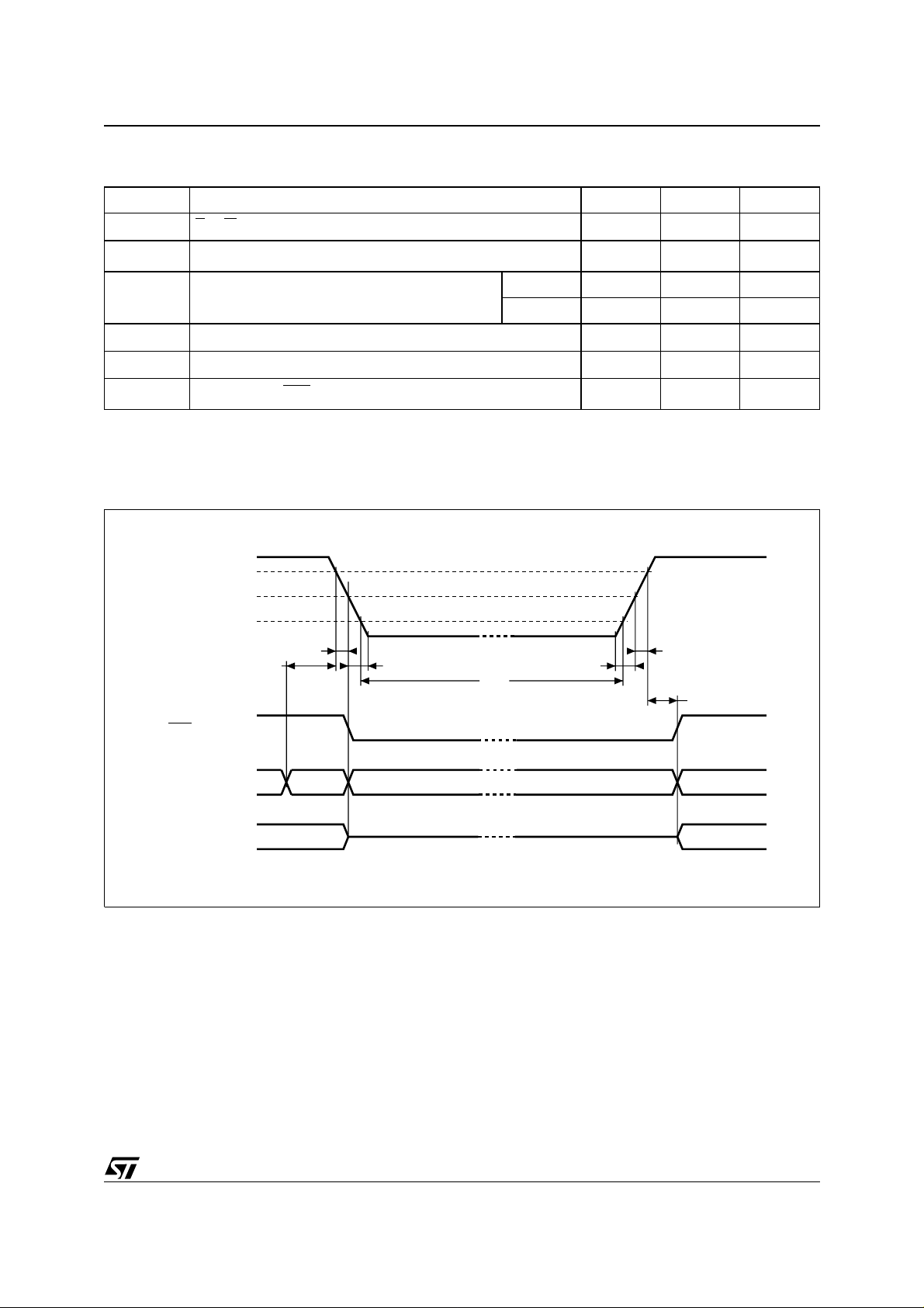
Figure 5. Power Down/Up Mode AC Waveforms
V
CC
V
(max)
PFD
V
(min)
PFD
VSO
tPD
tF
tFB
0 µs
300 µs
M48T59/Y 10 µs
M48T59V 150 µs
10 µs
1µs
40 200 ms
tR
tRB
tDR
tREC
RST
INPUTS
OUTPUTS
RECOGNIZED RECOGNIZED
VALID VALID
(PER CONTROL INPUT) (PER CONTROL INPUT)
The SOIC and battery/crystal packages are
shipped separately in plastic anti-static tubes or in
Tape & Reel form. For t he 2 8 le ad S OIC , t he ba ttery/crystal package (i.e. SNAPHAT) part number
is "M4T28-BR12SH" or “M4T32-BR12SH”.
Caution: Do not place the SNAPHAT battery/crys-
tal top in conductive foam, as this will drain the lithium button-cell battery.
As Figure 3 shows, the static memory array and
the quartz controlled clock oscillator of the
M48T59/59Y/59V are integrated on one silicon
chip.
DON'T CARE
HIGH-Z
AI03258
The two circuits are interconnected at the upper
eight memory locations to provide user accessible
BYTEWIDE™ clock information in the by tes with
addresses 1FF8h-1FFFh. The clock locations
contain the century, year, m ont h, d ate, day , hour,
minute, and second in 24 hour BCD format (except
for the century). Corrections for 28, 29 (leap year),
30, and 31 day months are made a utomatically.
Byte 1FF8h is the clock control register. This b yte
controls user access to the clock information and
also stores the clock calibration setting.
5/21
M48T59, M48T59Y, M48T59V
Table 9. Read Mode AC Characteristics
(T
= 0 to 70 °C or –40 to 85 °C; VCC = 4.75V to 5.5V or 4.5V to 5.5V or 3.0V to 3.6V)
A
M48T59/M48T5 9Y/M 48T5 9V
Symbol Parameter
t
AVAV
t
AVQV
t
ELQV
t
GLQV
t
ELQX
t
GLQX
t
EHQZ
t
GHQZ
t
AXQX
Note: 1. CL = 100pF (see Fig 4).
2. C
Read Cycle Time 70 ns
(1)
Address Valid to Output Valid 70 ns
(1)
Chip Enable Low to Output Valid 70 ns
(1)
Output Enable Low to Output Valid 35 ns
(2)
Chip Enable Low to Output Transition 5 ns
(2)
Output Enable Low to Output Transition 5 ns
(2)
Chip Enable High to Output Hi-Z 25 ns
(2)
Output Enable High to Output Hi-Z 25 ns
(1)
Address Transition to Output Transition 10 ns
= 5pF (see Fig 4).
L
Figure 6. Read Mode AC Waveforms.
Unit-70
Min Max
A0-A12
E
G
DQ0-DQ7
Note: Write Enable (W
6/21
) = High.
tAVAV
VALID
tAVQV tAXQX
tELQV
tELQX
tGLQX
tGLQV
tGHQZ
VALID
tEHQZ
AI01385
M48T59, M48T59Y, M48T59V
Table 10. Write Mode AC Characteristics
(T
= 0 to 70 °C or –40 to 85 °C; VCC = 4.75V to 5.5V or 4.5V to 5.5V or 3.0V to 3.6V)
A
M48T59/M48T 59Y/M 48T59V
Symbol Parameter
t
AVAV
t
AVWL
t
AVEL
t
WLWH
t
ELEH
t
WHAX
t
EHAX
t
DVWH
t
DVEH
t
WHDX
t
EHDX
(1, 2)
t
WLQZ
t
AVWH
t
AVE1H
(1, 2)
t
WHQX
Note: 1. CL = 5pF (see Fig 4).
2. If E
Write Cycle Time 70 ns
Address Valid to Write Enable Low 0 ns
Address Valid to Chip Enable Low 0 ns
Write Enable Pulse Width 50 ns
Chip Enable Low to Chip Enable High 55 ns
Write Enable High to Address Transition 0 ns
Chip Enable High to Address Transition 0 ns
Input Valid to Write Enable High 30 ns
Input Valid to Chip Enable High 30 ns
Write Enable High to Input Transition 5 ns
Chip Enable High to Input Transition 5 ns
Write Enable Low to Output Hi-Z 25 ns
Address Valid to Write Enable High 60 ns
Address Valid to Chip Enable High 60 ns
Write Enable High to Output Transition 5 ns
goes low simultaneously with W going l ow, the output s remain in the h i gh i m pedance state.
Unit-70
Min Max
The eight clock bytes are not the actual clock
counters themselves; they are memory locat ions
consisting of BiPORT™ read/ write memory cells.
The M48T59/59Y/59V includes a clock control circuit which updates the clock bytes with current information once per second. The information can
be accessed by the user in the same manner as
any other location in the static memory array.
The M48T59/59Y/59V also ha s its own P ower-fail
Detect circuit. The control circuitry constantly monitors the single 5V supply for an out of tolerance
condition. When V
is out of tolerance, the circuit
CC
write protects the S RAM, p roviding a high degree
of data security in the midst of unpredictable s ystem operation brought on by low V
. As VCC falls
CC
below approximately 3V, the control circuitry connects the battery which maintains data and clock
operation until valid power returns.
READ MODE
The M48T59/59Y/59V is in the Read Mode whenever W
(Write Enable) is high and E (Chip Enable)
is low. The unique address specified by the 13 Address Inputs defines which one of the 8,192 bytes
of data is to be acces sed. Valid data will be available at the Data I/O pi ns within Address Access
time (t
stable, providing that the E
are also satisfied. If the E
) after the last address input s ignal is
AVQV
and G access times
and G access times are
not met, valid data will be available after the latter
of the Chip Enable Access time (t
Enable Access time (t
GLQV
).
ELQV
) or Output
The state of the eight t hree-s tate Da ta I/O s i gnals
is controlled by E
ed before t
indeterminate state until t
puts are changed while E
and G. If the outputs are activat-
, the data lines will be driven to an
AVQV
. If the Ad dres s In-
AVQV
and G remain active,
output dat a will rem ain v alid for Outp ut Dat a Hold
time (t
) but will go indeterminate until the next
AXQX
Addr e ss Access.
7/21
 Loading...