

SGS Thomson Microelectronics M48T58Y, M48T58, M48T58Y-70PC1, M48T58Y-70MH1 Datasheet
64 Kbit (8Kb x8) TIMEKEEPER® SRAM
INTEGRATED ULTRA LOW POWER SRAM,
REAL TIME CLOCK , PO WE R-FAIL CONTRO L
CIRCUIT and BA T TER Y
BYTEWIDE RAM-LIKE CLOCK ACCE S S
BCD CODED YEAR, MONTH, DAY, DATE,
HOURS, MINUTES and SECONDS
FREQUENCY TEST OUTPUT for REAL TIME
CLOCK
AUTOMATIC POW ER-F AIL CH IP DES ELECT and
WRITE PROTECTION
WRITE PROTECT VOLT AGES
(V
= Power-fail Deselect Voltage):
PFD
– M48T58: 4.5V ≤ V
– M48T58Y: 4.2V ≤ V
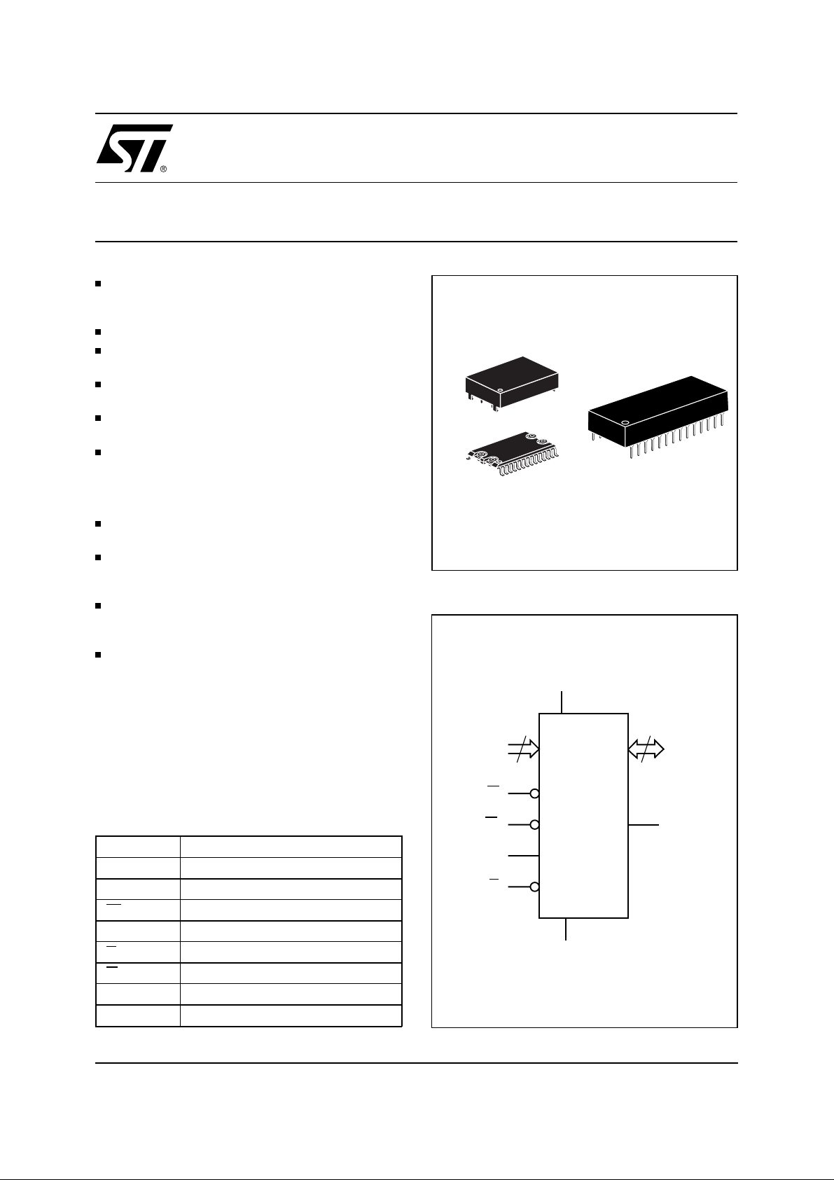
SELF-CONTAINED BA T TER Y and CRYSTAL
in the CAPHAT DIP PACKAGE
PACKAGING INCLUDES a 28-LEAD SOIC
and SNAPHAT
®
TOP
(to be Ordered Separately)
SOIC PACKAGE PROVIDES DIRECT
CONNECTION for a SNAPHAT TOP which
CONTAINS the BATTERY and CRYSTAL
PIN and FUNCTION COMPATIBLE with
JEDEC STANDARD 8K x 8 SRAMs
PFD
PFD
4.75V
≤
≤
4.5V
SNAPHAT (SH)
Battery/Crystal
28
28
1
SOH28 (MH)
Figure 1. Logic Diagram
V
CC
M48T58
M48T58Y
1
PCDIP28 (PC)
Battery/Crystal
CAPHAT
DESCRIPTION
The M48T58/58Y TIMEK E EPE R
®
RAM is an 8K x
8 non-volatile static RAM and real time clock. The
monolithic chip is available in two special packages
A0-A12
13
8
DQ0-DQ7
to provide a highly integrated battery backed-up
memory and real time clock solution.
T ab le 1. Signal Names
A0-A12 Address Inputs
DQ0-DQ7 Data Inputs / Outputs
FT Frequency Test Output (Open Drain)
E1 Chip Enable 1
E2 Chip Enable 2
G Output Enable
W Write Enable
V
CC
V
SS
July 1999 1/17
Supply Voltage
Ground
W
E1 FT
E2
G
M48T58
M48T58Y
V
SS
AI01374B
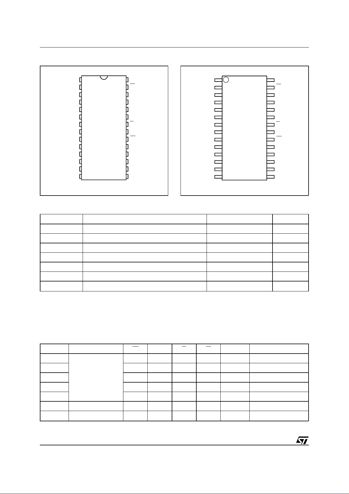
M48T58, M48T58Y
Figure 2A. DIP Pin Connections
FT V
1
A12
2
3
A7
4
A6
5
A5
6
A4
7
A3
A2
A1
A0
DQ0
8
9
10
11
M48T58
M48T58Y
12
13
DQ2
14
SS
28
27
26
25
24
23
22
21
20
19
18
17
16
15
AI01375B
CC
W
E2
A8
A9
A11
G
A10
E1
DQ7
DQ6
DQ5DQ1
DQ4
DQ3V
T ab le 2. Absolute Maximum Ratings
(1)
Figure 2B. SOIC Pin Connections
1
FT V
A12
DQ0
A7
A6
A5
A4
A3
A2
A1
A0
2
3
4
5
6
7
M48T58Y
8
9
10
11
12
DQ2
SS
13
14
28
27
26
25
24
23
22
21
20
19
18
17
16
15
AI01376B
Symbol Parameter Value Unit
T
A
T
STG
(2)
T
SLD
V
IO
V
CC
I
O
P
D
Notes:
1. Stresses greater than those listed under "Absolute Maximum Ratings" may cause permanent damage to the device. This is a
stress rating only and functional operation of the device at these or any other conditions above those indi cat ed in the operati onal
section of this specification is not implied. Exposure to the absolute maximum rating conditions for extended periods of time may
affect reliability.
2. Soldering temperature not to exceed 260°C for 10 seconds (total thermal budget not to exceed 150°C for longer than 30 seconds).
CAUTION: Negat i ve undershoots below –0.3 volts are not allowed on any pin while in the Battery Back-up mode.
CAUTION: Do NOT wave solder SOIC to avoid damaging SNAPHAT sockets.
T ab le 3. Operating Modes
Ambient Operating Temperature 0 to 70 °C
Storage T emper ature (VCC Off, Oscillator Off) –40 to 85 °C
Lead Solder Temperature for 10 seconds 260 °C
Input or Output Voltages –0.3 to 7 V
Supply Voltage –0.3 to 7 V
Output Current 20 mA
Power Dissipation 1 W
(1)
CC
W
E2
A8
A9
A11
G
A10
E1
DQ7
DQ6
DQ5DQ1
DQ4
DQ3V
Mode V
CC
Deselect
Deselect X V
Write V
4.75V to 5.5V
or
4.5V to 5.5V
Read V
Read V
Deselect V
SO
to V
Deselect ≤ V
Notes
:1. X = V
2. See Table 7 for details.
or VIL; VSO = Battery Back-up Switchover Voltage.
IH
PFD
(min)
SO
(2)
E1 E2 G W DQ0-DQ7 Power
V
IH
IL
IL
IL
X X X X High Z CMOS Standby
X X X X High Z Battery Back-up Mode
2/17
X X X High Z Standby
IL
V
IH
V
IH
V
IH
X X High Z Standby
XVILD
V
IL
V
IH
V
IH
V
IH
IN
D
OUT
High Z Active
Active
Active
Figure 3. Block Diagram
M48T58, M48T58 Y
FT
OSCILLATOR AND
CLOCK CHAIN
32,768 Hz
CRYSTAL
POWER
LITHIUM
CELL
VOLTAGE SENSE
AND
SWITCHING
CIRCUITRY
V
CC
DESCRIPTION
(cont’d)
The M48T58/58Y is a non-volatile pin and function
equivalent to any JEDEC standard 8K x 8 SRAM.
It also easily fits into many ROM, EPROM, and
EEPROM sockets, providing the non-volatility of
PROMs without any requirement for special write
timing or limitations on the number of writes t hat
can be performed.
The 28 pin 600mil DIP CAPHAT houses the
M48T58/58Y silicon with a quartz crystal and a long
life lithium button cell in a single package.
The 28 pin 330mil SOIC provides s ockets with gold
plated contacts at both ends for direct connection
to a separate SNAPHAT housing containing the
battery and crystal. The unique design allows the
SNAPHAT battery package to be mounted on top
of the SOIC package after the completion of the
surface mount process. Insertion of the SNAPHAT
housing after reflow prevents potential battery and
crystal damage due to the hig h temperatures required for device surface-mounting. The SNAPHA T
housing is keyed to prevent reverse insertion.
The SOIC and battery/crystal packages are
shipped separately in plastic anti-static tubes or in
Tape & Reel form.
8 x 8 BiPORT
SRAM ARRAY
A0-A12
DQ0-DQ7
E1
E2
W
G
AI01377C
V
PFD
8184 x 8
SRAM ARRAY
V
SS
Table 4. AC Measurement Conditions
Input Rise and Fall Times ≤ 5ns
Input Pulse Voltages 0 to 3V
Input and Output Timing Ref. Voltages 1.5V
Note that Output Hi-Z is defined as the point where data is no
longer driven.
Figure 4. AC Testing Load Circuit
5V
1.9kΩ
DEVICE
UNDER
TEST
1kΩ
CL includes JIG capacitance
CL = 100pF or 5pF
OUT
AI01030
3/17
M48T58, M48T58Y
(1, 2)
T ab le 5. Capacitance
= 25 °C, f = 1 MHz )
(T
A
Symbol Parameter T est Condition Min Max Unit
C
IN
(3)
C
IO
Notes:
1. Effective capacitance measured with power supply at 5V .
2. Sampled only, not 100% tested.
3. Outputs deselected
Input Capacitance VIN = 0V 10 pF
Input / Output Capacitance V
= 0V 10 pF
OUT
T ab le 6. DC Characteristics
= 0 to 70°C; VCC = 4.75V to 5.5V or 4.5V to 5.5V)
(T
A
Symbol Parameter Test Condition Min Max Unit
(1)
I
LI
(1)
I
LO
Supply Current Outputs open 50 mA
I
CC
I
CC1
I
CC2
(2)
V
IL
V
IH
V
OL
V
OH
Notes:
1. Outputs Deselected.
2. Negative spikes of –1V allowed for up to 10ns once per Cycle.
3. The FT pin is Open Drain.
T able 7. Power Down/Up Trip Points DC Characteristics
= 0 to 70°C)
(T
A
Input Leakage Current 0V ≤ VIN ≤ V
Output Leakage Current 0V ≤ V
Supply Current (Standby) TTL E1 = VIH, E2 = V
Supply Current (Standby) CMOS
E1 = VCC – 0.2V,
E2 = V
OUT
SS
CC
≤ V
CC
+ 0.2V
IL
Input Low Voltage –0.3 0.8 V
Input High Voltage 2.2 VCC + 0.3 V
Output Low Voltage I
Output Low Voltage (FT)
(3)
= 2.1mA 0.4 V
OL
IOL = 10mA 0.4 V
Output High Voltage IOH = –1mA 2.4 V
(1)
±1 µA
±5 µA
3mA
3mA
Symbol Parameter Min Typ Max Unit
V
PFD
V
PFD
V
SO
t
DR
Notes:
1. All voltages referenced to V
2. At 25°C
DESCRIPTION
For the 28 lead SOIC, the battery/crystal package
(i.e. SNAPHAT) part number is "M4T28BR12SH1".
As Figure 3 shows, the static memory array and the
quartz controlled clock oscillator of the
M48T58/58Y are integrated on one silicon chip.
The two circuits are interconnected at the upper
eight memory locations to provide user accessible
Power-fail Deselect Voltage (M48T58) 4.5 4.6 4.75 V
Power-fail Deselect Voltage (M48T58Y) 4.2 4.35 4.5 V
Battery Back-up Switchover Voltage 3.0 V
(2)
Expected Data Retention Time 7 YEARS
.
SS
(cont’d)
BYTEWIDE clock information in the bytes with
addresses 1FF8h-1FFFh. The clock locations contain the year, month, date, day, hour, minute, and
second in 24 hour BCD format. Corrections for 28,
29 (leap year), 30, and 31 day months are made
automatically. Byte 1FF8h is the clock control register. This byte controls user access to the clock
information and also stores the clock calibration
setting.
4/17
M48T58, M48T58 Y
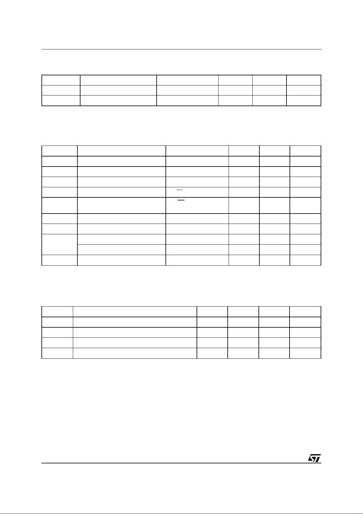
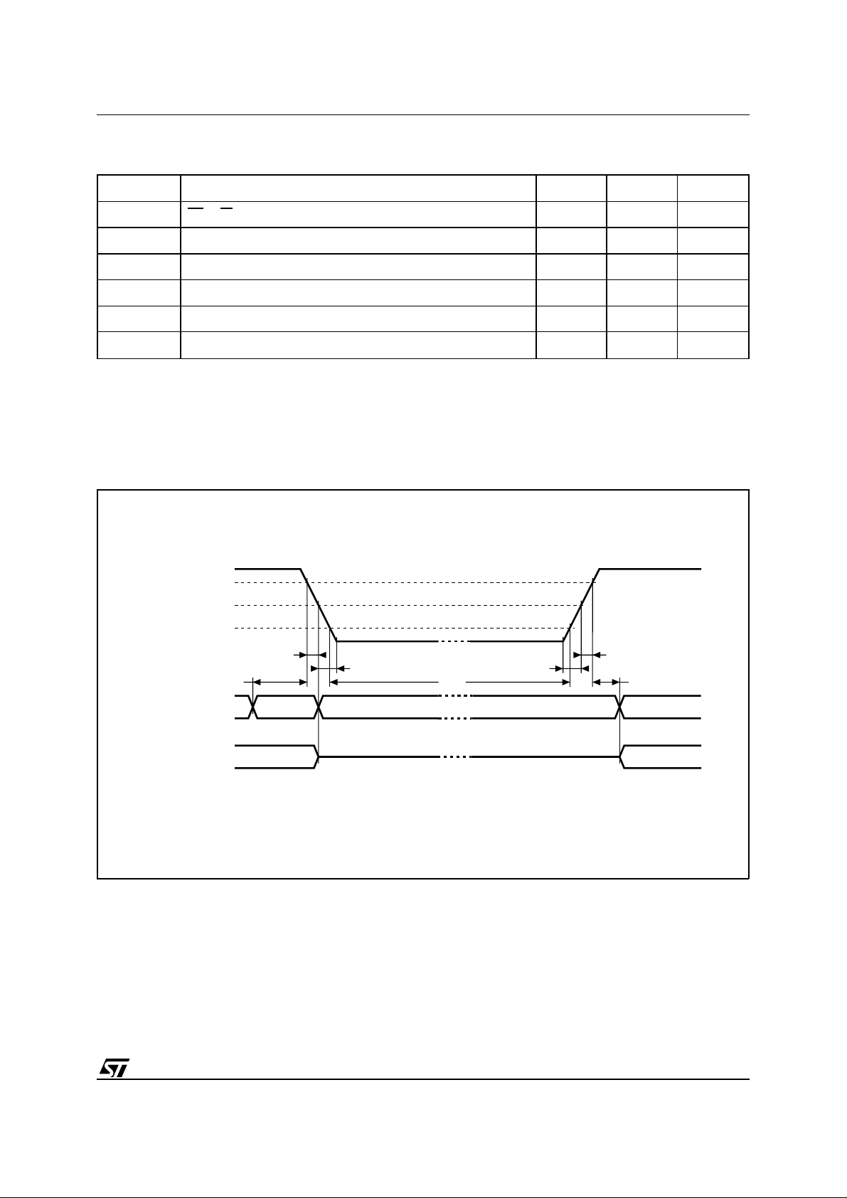
T able 8. Power Down/Up Mode AC Characteristics
= 0 to 70°C)
(T
A
Symbol Parameter Min Max Unit
E1 or W at VIH or E2 at VIL before Power Down 0 µs
V
(max) to V
PFD
V
(min) to VSO VCC Fall Time 10 µs
PFD
V
(min) to V
PFD
VSO to V
V
(max) to V
PFD
passes V
CC
(min) to VSO fall time of less than tFB may cause corruption of RAM data.
PFD
PFD
(max) to Inputs Recognized 40 200 ms
PFD
(min) fall time of less than tF may result in deselection/writ e protection not occ urri ng until 200 µs after
PFD
(min).
PFD
(min) VCC Fall Time 300 µs
PFD
(max) VCC Rise Time 10 µs
PFD
(min) VCC Rise Time 1 µs
Notes
t
PD
(1)
t
F
t
FB
t
R
t
RB
t
REC
:1.V
2. V
(2)
V
Figure 5. Power Down/Up Mode AC Waveforms
V
CC
V
(max)
PFD
V
(min)
PFD
VSO
INPUTS
OUTPUTS
tF
tPD
VALID VALID
(PER CONTROL INPUT)
tFB
tDR
tRB
DON'T CARE
HIGH-Z
tR
tREC
RECOGNIZEDRECOGNIZED
(PER CONTROL INPUT)
AI01168C
5/17
M48T58, M48T58Y
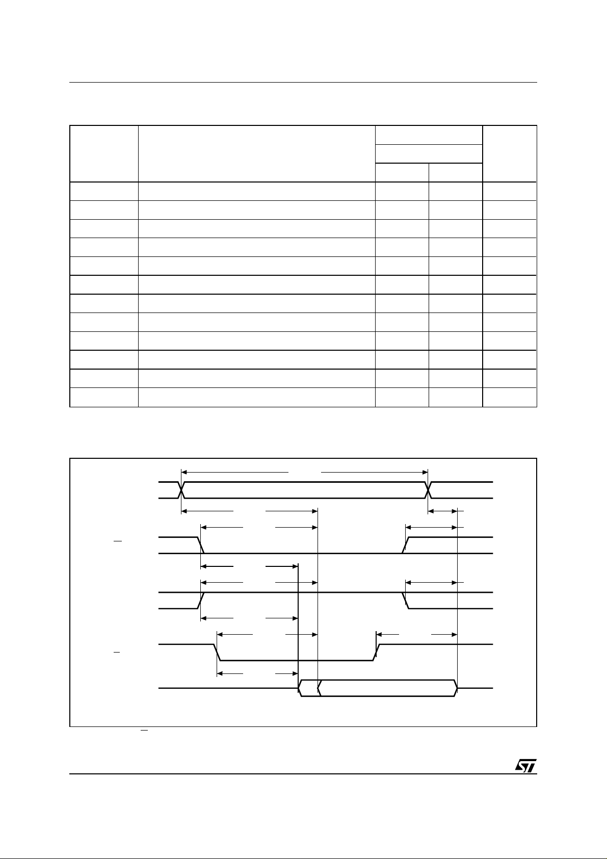
T ab le 9. Read Mode AC Characteristics
= 0 to 70°C; VCC = 4.75V to 5.5V or 4.5V to 5.5V)
(T
A
Symbol Parameter
Notes:
t
AVAV
(1)
t
AVQV
(1)
t
E1LQV
t
E2HQV
(1)
t
GLQV
(2)
t
E1LQX
t
E2HQX
(2)
t
GLQX
(2)
t
E1HQZ
(2)
t
E2LQZ
(2)
t
GHQZ
(1)
t
AXQX
1. C
= 100pF (see Figure 4).
L
= 5pF (see Figure 4).
2. C
L
Read Cycle Time 70 ns
Address Valid to Output Valid 70 ns
Chip Enable 1 Low to Output Valid 70 ns
(1)
Chip Enable 2 High to Output Valid 70 ns
Output Enable Low to Output Valid 35 ns
Chip Enable 1 Low to Output Transition 5 ns
(2)
Chip Enable 2 High to Output Transition 5 ns
Output Enable Low to Output Transition 5 ns
Chip Enable 1 High to Output Hi-Z 25 ns
Chip Enable 2 Low to Output Hi-Z 25 ns
Output Enable High to Output Hi-Z 25 ns
Address Transition to Output Transitio n 10 ns
M48T58 / M48T58Y
-70
Min Max
Unit
Figure 6. Read Mode AC Waveforms
A0-A12
E1
tE1LQX
E2
tE2HQX
G
DQ0-DQ7
Note:
Write Enable (
W) = High.
tAVAV
VALID
tAVQV tAXQX
tE1LQV
tE2HQV
tGLQV
tGLQX
tGHQZ
VALID
tE1HQZ
tE2LQZ
AI00962
6/17
 Loading...