

M48T559Y
64 Kbit (8Kb x8) TIMEKEEPER® SRAM
with ADDRESS/DATA MULTIPLEXED
■ SOFTWARE and HARDWARE RESET for
WATCHDOG T IM ER
■ REGISTER COMPATIBLE with M48T59
TIMEKEEPER SRAM
■ ADDRESS/DATA MULTIPL EXED I/O PINS
■ WATCHDOG TIMER - MONITORS OUT of
CONTROL PROCESSOR or HUNG BU S
■ ALARM with WAKE-UP in BATTERY MODE
■ INTEGRATED ULTRA LOW POWER SRAM,
REAL TIME CLOCK, POWER-FAIL CONTROL
CIRCUIT and BATTERY
■ FREQUENCY TEST OUTPUT for REAL TIME
CLOCK
■ AUTOMATIC POWER-FAIL CHIP DESELECT
and WRITE PROTECTION
■ WRITE PROTECT VOLTAGE
(V
= Power-fail Deselect Voltage):
PFD
– M48T559Y: 4.2V ≤ V
■ PACKAGING INCLU DES a 28- L EAD SOIC
and SNAPHAT
®
TOP
PFD
≤ 4.5V
(to be Ordered Separately)
■ SOIC PACKAGE PROVIDES D IREC T
CONNECTION for a SNAPHAT TOP
CONTAINS the BATTERY and CRYSTAL
■ MICROPROCESSOR POWER-ON RESET
(Valid even during battery back-up mode)
■ PROGRAMM ABLE A L A R M O U TPUT ACTIVE
in the BATTERY BACK-UP MODE
SNAPHAT (SH)
Battery/Crystal
28
1
SOH28 (MH)
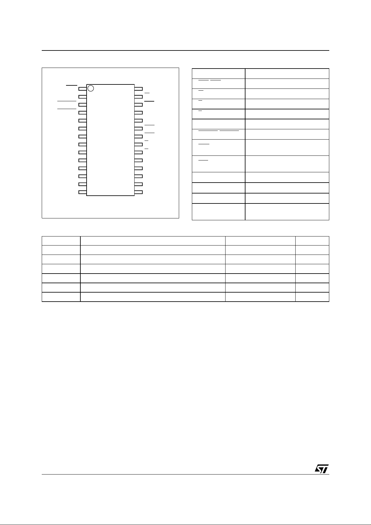
Figure 1. Logic Diagram
V
CC
AS0
AS1
W
R
RSTIN1
M48T559Y
8
AD0-AD7
RST
IRQ/FT
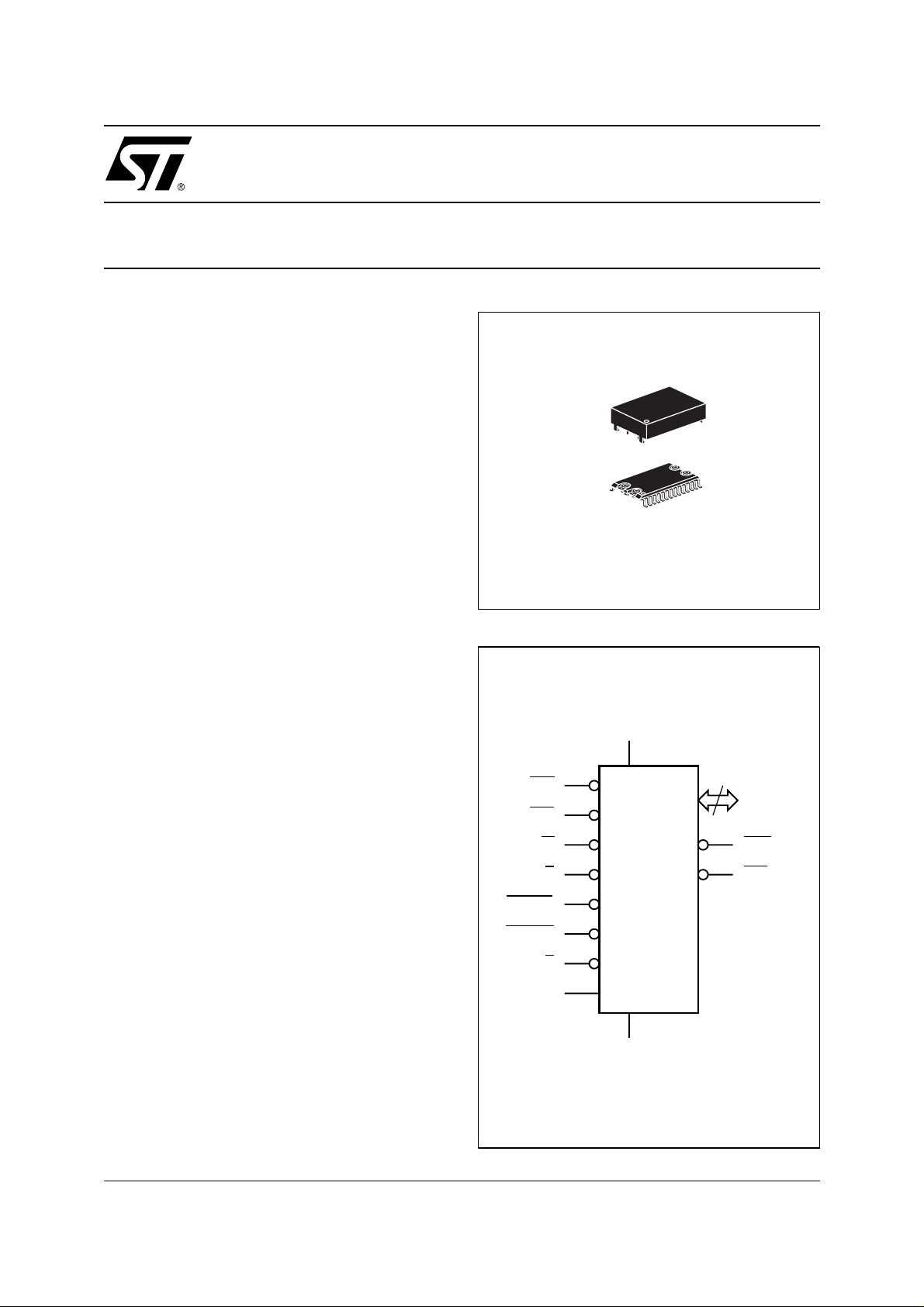
DESCRIPTION
The M48T559Y TI MEKEEPER
®
RAM is an 8K x 8
non-volatile static RAM and real time clock. The
monolithic chip is available in the SNAPHAT package to provide a highly integrated battery backedup memory and real time clock solution.
The 28 pin 330mil SOIC provides sockets with
gold plated contacts at both ends for direct connection to a separate SNAPHAT housing cont aining the battery and crystal. The unique design
allows the SNAPHAT battery package to be
mounted on top of the SOIC package after the
completion of the surface mount process.
RSTIN2
WDI
E
V
SS
AI01674B
1/18February 2000
M48T559Y
Figure 2. SOIC Connections
RST V
WDI
RSTIN1
RSTIN2
DU
NC
NC
NC
NC
AD0
AD1
V
SS
SS
1
2
3
4
5
6
7
M48T559Y
8
9
10
11
12
13
14
AI01675B
28
27
26
25
24
23
22
21
20
19
18
17
16
15
CC
W
IRQ/FT
DU
DU
AS1
AS0
R
E
AD7
AD6
AD5AD2
AD4
AD3V
Table 1. Signal Names
AD0-AD7 Address/Data
AS0
-AS1 Address Strobes
W
R
E
WDI Watchdog Input
RSTIN1
RST
IRQ
V
V
NC Not Connected Internally
DU
-RSTIN2 Reset Input
/FT
CC
SS
Write Enable
Read Enable
Chip Enable
Power Fail Reset Output
(Open Drain)
Interrupt / Frequency Test
Output (Open Drain)
Supply Voltage
Ground
Don’t Use must be connected
or V
to V
CC
SS
Table 2. Absolute Maximum Ratings
Symbol Parameter Value Unit
T
A
T
STG
V
IO
V
CC
I
O
P
D
Note: Stress es greate r than t hose listed unde r "Absolute Maxi m um Ratings" may c ause perm anent damage to the device. This is a stress
rating onl y and fun ct i onal oper at i on of the device at these or any other conditions above t hose indicated in the operat i onal section of
this specification is not implied. Exposure to the absolute maximum rating conditions for extended periods of time may affect reliability.
CAUTION: Negative undershoo ts bel ow –0.3V are not allowed on any pi n while in the B at tery Back- up mode.
CAUTION: Do NOT wave solder SOIC to avoid damaging SNAPHAT sockets.
Ambient Operating Temperature 0 to 70 °C
Storage Temperature (VCC Off, Oscillator Off)
Input or Output Voltages –0.3 to 7 V
Supply Voltage –0.3 to 7 V
Output Current 20 mA
Power Dissipation 1 W
–40 to 85 °C
Insertion of the SNAPHAT housing after reflow
prevents potential battery and crystal damage due
to the high temperatures required for device surface-mounting. The SNAPHAT housing is keyed
to prevent reverse insertion.
The SOIC and battery/crystal packages are
shipped separately in plastic anti-static tubes or in
Tape & Reel form. For t he 2 8 le ad S OIC , t he ba ttery/crystal package (i.e. SNAPHAT) part number
is "M4T28-BR12SH1".
Caution: Do not place the SNAPHAT battery/crystal top in conductive foam, as this will drain the lithium button-cell battery.
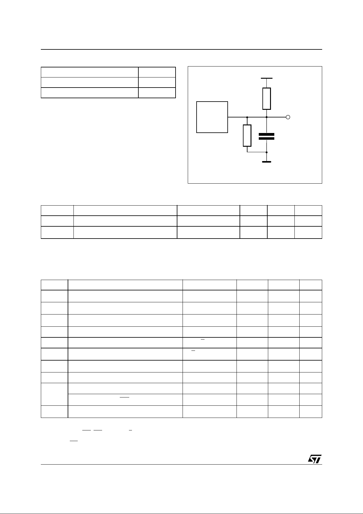
As Figure 3 shows, the static memory array and
the quartz controlled clock oscillator of the
M48T559Y are integrated on one silicon chip. The
2/18
two circuits are interconnected at the up per eight
memory locations to provide user accessible
BYTEWIDE™ clock information in the by tes with
addresses 1FF8h-1FFFh. The clock locations
contain the year, month, date, day, ho ur, minute,
and second in 24 hour BCD format. Corrections for
28, 29 (leap year), 30, and 31 day months are
made automatically. Byte 1FF8h is the clock control register. This byte controls us er ac cess to t he
clock information and also stores the clock calibration setting.
The eight clock bytes are not the actual clock
counters themselves; they are memory locations
consisting of BiPORT™ read/write memory cells.
The M48T559Y includes a clock control circuit
which updates the clock bytes with current infor-
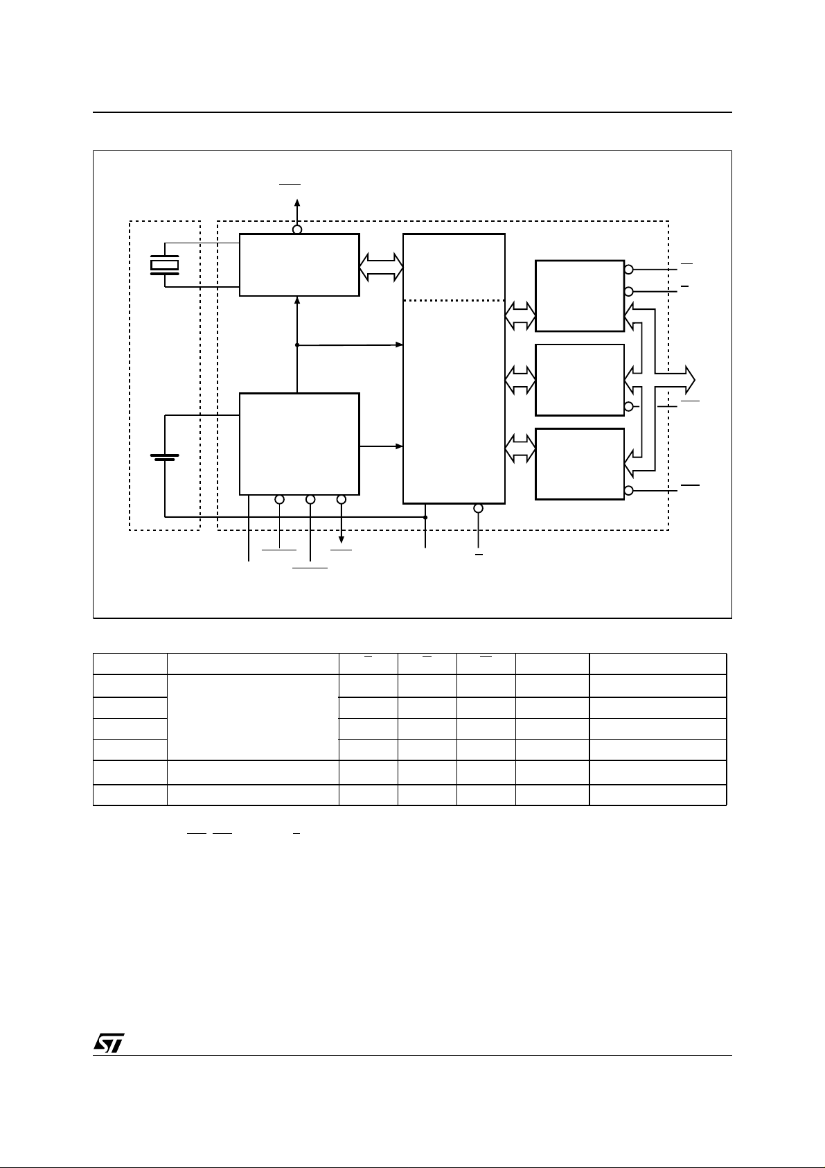
Figure 3. Block Diagram
M48T559Y
IRQ/FT
OSCILLATOR AND
CLOCK CHAIN
32,768 Hz
CRYSTAL
POWER
LITHIUM
CELL
VOLTAGE SENSE
AND
SWITCHING
CIRCUITRY
RSTIN1
V
CC
Table 3. Operating Modes
Mode
V
CC
RSTIN2
(1)
Deselect
Write
4.5V to 5.5V
Read
Read
Deselect
Deselect
Note: 1. X = VIH or VIL; VSO = Battery Back-up Swit ch ov er Volta ge.
2. See Table 7 for details.
3. AD0-AD7, AS0
V
to V
SO
PFD
≤ V
SO
, AS1 active when E is high and VCC > V
(min)
(2)
V
PFD
RST
E R W AD0-AD7 Power
V
IH
V
IL
V
IL
V
IL
X X X High Z CMOS Standby
X X X High Z Battery Back-up Mode
PFD
16 x 8 BiPORT
SRAM ARRAY
8176 x 8
SRAM ARRAY
V
SS
E
X X High Z
V
IH
V
IL
V
IH
.
V
IL
V
IH
V
IH
DATA
TRANSCEIVER
UPPER
ADDRESS
LATCH
LOWER
ADDRESS
LATCH
AD0-AD7
Standby
D
D
OUT
IN
Active
Active
High Z Active
W
R
AS1
AS0
AI01676B
(3)
mation once per second. The information can be
accessed by the user i n t he sa me m anner as any
other location in the static memory array.
The M48T559Y also has its own Power-fail Detect
circuit. The control circuitry constantly monitors
the single 5V supply for an out of tolerance condition.
When VCC is out of tolerance, the circuit write protects the SRAM, providing a h igh degree of data
security in the midst of unpredictable system operation brought on by low V
. As VCC falls be low
CC
approximately 3V, the control circuitry connects
the battery which maintains data and clock operation until valid power returns.
3/18
M48T559Y
Table 4. AC Measurement Conditions
Input Rise and Fall Times ≤ 5ns
Figure 4. AC Testing Load Circuit
5V
Input Pulse Voltages 0 to 3V
Input and Output Timing Ref. Voltages 1.5V
Note that Output Hi-Z is defined as the point where data is no longer
driven.
Table 5. Capacitance
= 25 °C, f = 1 MHz)
(T
A
(1, 2)
DEVICE
UNDER
TEST
1kΩ
CL includes JIG capacitance
1.9kΩ
OUT
CL = 100pF
Symbol Parameter Test Condition Min Max Unit
V
V
IN
OUT
= 0V
= 0V
10 pF
10 pF
C
IN
C
IO
Note: 1. Effectiv e capacitance measured with power suppl y at 5V .
2. Sampled only, not 100% tested.
3. Outputs deselected.
Input Capacitance
(3)
Input / Output Capacitance
AI01673
Table 6. DC Characteristics
= 0 to 70 °C; VCC = 4.5V to 5.5V)
(T
A
Symbol Parameter Test Condition Min Max Unit
(1)
Input Leakage Current
I
LI
(1)
I
LO
I
LRST
I
I
CC1
I
CC2
V
IL
V
Output Leakage Current
(2)
Input Leakage Current
Supply Current Outputs open 50 mA
CC
Supply Current (Standby) TTL
(3)
Supply Current (Standby) CMOS
(4)
Input Low Voltage –0.3 0.8 V
Input High Voltage 2.2
IH
Output Low Voltage
V
OL
Output Low Voltage (IRQ
(6)
V
OH
Note: 1. Outputs deselected.
Output High Voltage
2. Input leakage current on input RESET p i ns.
3. AD0-AD7, AS0
4. Ne ga t i ve spik e s of –1V allo wed for up t o 10 ns once pe r cycle .
5. The IRQ
6. Measured with Control Bits set as follows: R = '1'; W, ST , FT = '0'.
, AS1 active when E is high and VCC > V
pins is Open Drain.
/FT)
(5)
PFD
0V ≤ V
0V ≤ V
0V ≤ V
E
.
≤ V
IN
CC
≤ V
OUT
≤ V
IN
CC
E
= V
IH
= VCC – 0.2V
I
= 2.1mA
OL
IOL = 10mA
I
= –1mA
OH
CC
±1 µA
±5 µA
100 µA
10 mA
7mA
V
+ 0.3
CC
0.4 V
0.4 V
2.4 V
V
4/18
M48T559Y
Table 7. Power Down/Up Trip Points DC Characteristics
(1)
(TA = 0 to 70 °C)
Symbol Parameter Min Typ Max Un it
V
PFD
V
SO
t
DR
Note: 1. All voltages referenced to VSS.
2. At 25°C.
Power-fail Deselect Voltage 4.2 4.35 4.5 V
Battery Back-up Switchover Voltage 3.0 V
(2)
Expected Data Retention Time 7 YEARS
Table 8. Power Down/Up AC Characteristics
(T
= 0 to 70 °C)
A
Symbol Parameter Min Max Unit
t
PD
(1)
t
F
(2)
t
FB
t
R
t
RB
t
REC
Note: 1. V
2. V
PFD
es V
PFD
E at VIH before Power Down
V
(max) to V
PFD
V
(min) to VSS VCC Fall Time
PFD
V
(min) to V
PFD
VSS to V
V
(max) to V
(min).
PFD
(min) to VSS fall time of less than tFB may cause corruption of RAM data.
PFD
(max) to RST High
PFD
(min) fall time of less than tF may result in deselection/write protection not occurring until 200µs after VCC pass-
PFD
(min) VCC Fall Time
PFD
(max) VCC Rise Time
PFD
(min) VCC Rise Time
0 µs
300 µs
10 µs
10 µs
1µs
40 200 ms
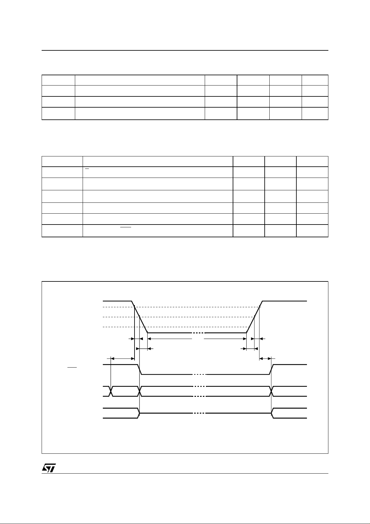
Figure 5. Power Down/Up Mode AC Waveforms
V
CC
V
(max)
PFD
V
(min)
PFD
VSO
tF
tFB
RST
INPUTS
OUTPUTS
VALID VALID
(PER CONTROL INPUT)
tDR
tRB
DON'T CARE
HIGH-Z
tR
tRECtPD
RECOGNIZEDRECOGNIZED
(PER CONTROL INPUT)
AI01384D
5/18
M48T559Y
Table 9. AC Characteristics
(T
= 0 to 70 °C; VCC = 4.5V to 5.5V)
A
Symbol Parameter
t
AS
t
AH
t
DS
t
DH
t
RLDV
t
RLRH
t
RHDZ
t
WLWH
t
ELEH
t
ASLASH
t
ASHRL
t
ASHWL
t
ELRL
t
EHDZ
t
ELWL
Address Setup Time 20 ns
Address Hold Time 0 ns
Data Setup Time 60 ns
Data Hold Time 0 ns
Read Enable Access Time 70 ns
R Pulse Width Low 70 ns
Read Enable High to Output High Z 25 ns
W Pulse Width Low 50 ns
E Pulse Width Low 50 ns
AS0, AS1 Pulse Width Low 15 ns
AS0, AS1 High to R Low 15 ns
AS0, AS1 High to W Low 15 ns
Chip Enable Low to Read Enable Low 0 ns
Chip Enable High to Data Output Hi-Z 0 ns
Chip Enable Low to Write Enable Low 0 ns
M48T559Y
Unit
Min Max
RAM OPERATION
Four control signals, AS0
, AS1, R and W, ar e us ed
to access the M48T559Y. The address latches are
loaded from the address/data b us in respon se to
rising edge signals applied to the Address Strobe
0 (AS0
) and Address Strobe 1 (AS1) signals. AS0
is used to latch the lower 8 b its of address, and
AS1
is used to latch the upper 5 bits of address.
It is not however necessary to follow any particular
order. The inputs are in parallel for the two address bytes (upper and lower) and can be latched
in any order as long as the correct strobe is used.
It is necessary to meet the set-up and hold times
given in the AC specifications with valid address
information in order to properly latch the address.
If the upper and/or lower order addresses are correct from a prior cycle, it is not necessary to repeat
the address latching sequence.
A write operation requires valid dat a to be placed
on the bus (AD0-AD7), followed by the activation
of the Write Enabl e (W
) line. Data on t he bus wi ll
be written to the RAM, provided that the write timing specific ations are met. During a read cycl e, the
Read Enable (R
) signal is driven active. Data from
the RAM will become valid on the bus provided
that the RAM read access timing specifications are
met.
The W
and R signals should never be active at the
same time. In addition, E
must be active before
any control line is recognized (except for AD0-AD7
and AS0
, AS1).
RESET INPUT
The M48T559Y provides two debounced inputs
which can generate an output Reset. The duration
and function of the Reset output is identical to a
Reset generated by a power cycle. Pulses shorter
than t
and tR2 will not generate a Reset condi-
R1
tion (see Table 12 and Figure 13).
DATA RETENTION MODE
Should the supply voltage decay, the RAM will automatically power-fail deselect, write protecting itself w hen V
falls within the V
CC
PFD
(max), V
PFD
(min) window. All outputs become high impedance, and all inputs are treated as "don't care."
Note: A power failure during a write cycle may corrupt data at the currently addressed location, but
does not jeopardize the rest of the RAM's content.
At voltages below V
(min), the user can be as-
PFD
sured the memory will be in a write protected state,
provided the V
fall time is no t les s than tF.
CC
6/18
 Loading...