

SGS Thomson Microelectronics M48T512V, M48T512Y-70PM1, M48T512Y Datasheet
3.3V-5V 4 Mbit (512Kb x8) TIMEKEEPER® SRAM
■ INTEGRATED ULTRA LOW POWER SRAM,
REAL TIME CLOCK, POWER-FAIL CONTROL
CIRCUIT, BATTERY, and CRYSTAL
■ BCD CODED YEAR, MONTH, DAY, DATE,
HOURS, MINUTES, and SECONDS
■ AUTOMATIC POWER-FAIL CHIP DESELECT
and WRITE PROTECTION
■ WRITE PROTECT VOLTAGES:
(V
= Power-fail Deselect Voltage)
PFD
– M48T512Y: 4.2V ≤ V
– M48T512V: 2.7V ≤ V
■ CONVENTIONAL SRAM OPERATION;
UNLIMITED WRITE CYCLES
■ SOFTWARE CONTROLLED CLOCK
CALIBRATION FOR HIGH ACCURACY
APPLICATIONS
■ 10 YEARS of DATA RETENTION and CLOCK
OPERATION in the ABSENCE OF POWER
■ PIN and FUNCTION COMPATIBLE with
INDUSTRY STANDARD 512K X 8 SRAMS
■ SELF-CONTAINED BATTERY and CRYSTA L
in DIP PACKAGE
PFD
PFD
≤ 4.5V
≤ 3.0V
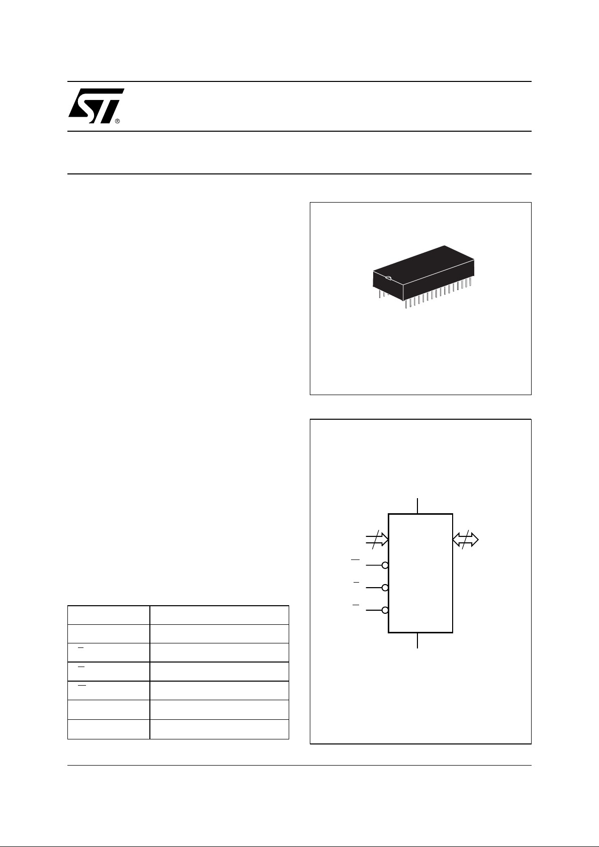
32
1
PMDIP32 (PM)
Module
Figure 1. Logic Diagram
V
CC
M48T512Y
M48T512V
DESCRIPTION
The M48T512Y/V TIMEKEEPER RAM is a 512Kb
x 8 non-volatile static RAM and real time clock organized as 524,288 words by 8 bits. The spe cial
DIP package provides a fully integrated battery
back-up memory and real time clock solution.
Table 1. Signal Names
A0-A18 Address Inputs
DQ0-DQ7 Data Inputs / Outputs
E
G
W
V
V
CC
SS
Chip Enable Input
Output Enable Input
Write Enable Input
Supply Voltage
Ground
19
A0-A18 DQ0-DQ7
W
E
G
M48T512Y
M48T512V
V
SS
8
AI02262
1/14December 1999
M48T512Y, M48T512V
Table 2. Absolute Maximum Ratings
Symbol Parameter Value Unit
T
A
T
STG
T
SLD
V
IO
V
CC
I
O
P
D
Note: 1. Stresses greater than those listed under "Absolute Maximum Ratings" may cause permanent damage to the device. This is a stress
2. Soldering temperature not to exceed 260°C for 10 seconds (total thermal budget not to exceed 150°C for longer than 30 seconds).
CAUTION: Negative undershoo ts bel ow –0.3V ar e not al l owed on any pin wh i l e i n the Batter y Back-up mod e.
Ambient Operating Temperature 0 to 70 °C
Storage Temperature (VCC Off, Oscillator Off)
(2)
Lead Solder Temperature for 10 seconds 260 °C
Input or Output Voltages
Supply Voltage
Output Current 20 mA
Power Dissipation 1 W
rating only and functional opera tion of the dev i ce at these or any other conditions above thos e i ndi cated in th e operational section
of this spec ification is not im plied. Exposure t o the abso lute max imum rat ing cond itions for extende d period s of tim e may affe ct
reliability.
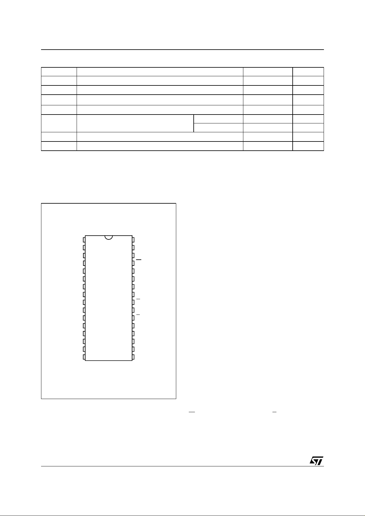
Figure 2. DIP C on ne ctions
(1)
–40 to 85 °C
–0.3 to V
M48T512Y –0.3 to 7.0 V
M48T512V –0.3 to 4.6 V
CC
+0.3
V
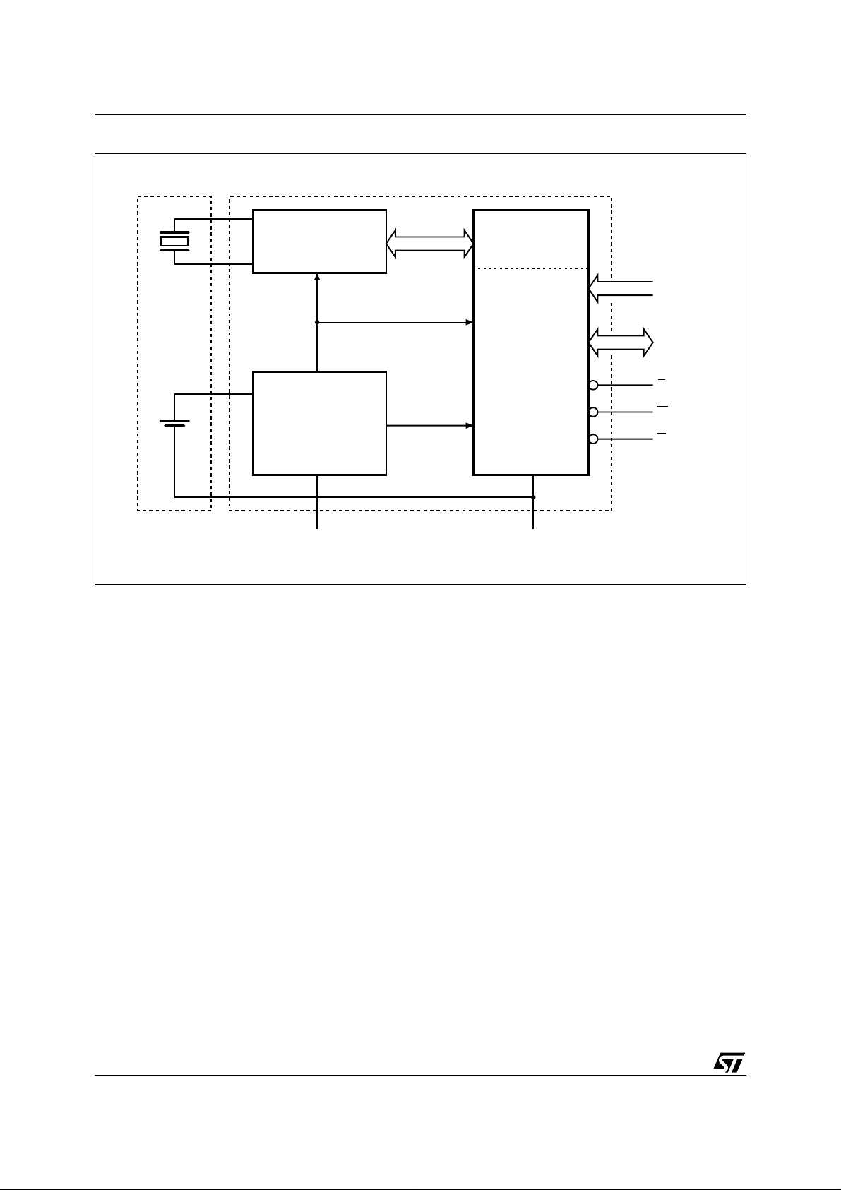
The 32 pin 600 mil DIP Hybrid houses a controller
chip, SRAM, quartz crystal, and a long life lithium
button cell in a single package. Figure 3 illustrates
the static memory array and the quartz con trolled
clock oscillator. The clock locations contain the
year, month, date, day, hour, minute, and second
A18 V
1
A16
2
3
A14
4
A12
5
A7
6
A6
7
A5
8
A4
A3
A2
A1
A0
DQ0
M48T512Y
M48T512V
9
10
11
12
13
14
15
DQ2
16
SS
32
31
30
29
28
27
26
25
24
23
22
21
20
19
18
17
AI02263
CC
A15
A17
W
A13
A8
A9
A11
G
A10
E
DQ7
DQ6
DQ5DQ1
DQ4
DQ3V
in 24 hour BCD format. Corrections for 28, 29
(leap year - compliant until the year 2100), 30, and
31 day months are made automatically. Byte
7FFF8h is the clock control register. This byte controls user access to the clock information and also
stores the clock calibration setting. The seven
clock bytes (7FFFFh-7FFF9h) are not the actual
clock counters, they are memory locations consist-
ing of BiPORT™ read/write memory cells within
the static RAM array. The M48T512Y/V includes a
clock control circuit which updates the clock bytes
with current information once per second. Th e information can be accessed by the user in the
same manner as any other location in the s tatic
memory array. The M48T512Y/V also has its own
Power-Fail Detect circuit. This control circuitry
constantly monitors the supply voltage for an out
of tolerance condition. When V
is out of toler-
CC
ance, the circuit write protects the TIMEKEEPER
register data and external SRAM, providi ng data
security in the midst of unpredictable system operation. As V
falls, the control circuitry automati-
CC
cally switches to the battery, maintaining data and
clock operation until valid power is restored.
The M48T512Y/V directly replaces industry standard 512Kb x 8 SRAMs. It also p rovides the nonvolatility of Flash without any requirement for special write timing or limitations on the number of
writes that can be performed.
2/14
READ MODE
The M48T512Y/V is in the Read Mode whenever
(Write Enable) is high and E (Chip Enable) is
W
low. The unique address specified by the 19 A ddress Inputs defines which one of the 524,288
bytes of data is to be access ed. Valid dat a will be
available at the D ata I/O pins within Address Ac-
M48T512Y, M48T512V
Table 3. Operating Modes
Mode
Deselect
Write
Read
Read
Deselect
Deselect
Note: 1. X = VIH or VIL.
2. See T able 7 for details.
cess T ime (t
AVQV
4.5V to 5.5V
3.0V to 3.6V
V
to V
SO
) after the last address input signal is stable, providing the E
are also satisfied. If the E
(1)
V
CC
or
(2)
(min)
PFD
(2)
≤ V
SO
and G access times
and G access times are
E G W DQ0-DQ7 Power
V
IH
V
IL
V
IL
V
IL
X X X High Z CMOS Standby
X X X High Z Battery Back-up Mode
not met, valid data will be available after the latter
of the Chip Enable Access Times (t
Enable Access Time (t
). The state of the eight
GLQV
three-state Data I/O signals is controlled by E
G
. If the outputs are activated before t
ELQV
) or Output
and
, the
AVQV
data lines will be driven t o an ind eterminate state
until t
while E
main valid for Output Data Hold Time (t
. If the Address Inputs are changed
AVQV
and G remain active, output data will re-
) but
AXQX
will go indeterminate until the next Address Access.
WRITE MODE
The M48T512Y/V is in the Wri te Mode whenever
(Write Enable) and E (Chip Enable) are low
W
state after the address inputs are stable. The start
of a write is referenced from the latter occurring
falling edge of W
earlier rising edge of W
be held valid throughout the cycle. E
turn high for a minimum of t
or t
from Write Enable prior to the initiation of
WHAX
or E. A write is terminated by the
or E. The addresses must
or W must r e-
from Chip Enable
EHAX
another read or write cycle. Data-in must be valid
prior to the end of write and remain valid for
t
DVWH
t
afterward. G should be kept high during
WHDX
write cycles to avoid bus c ontention; although, if
the output bus has been activated by a low on E
and G a low on W will disable the outputs t
ter W
falls .
WLQZ
af-
X X High Z Standby
X
V
IL
V
IH
V
IL
V
IH
V
IH
D
IN
D
OUT
High Z Active
Active
Active
Table 4. AC Measurement Conditions
Input Rise and Fall Times ≤ 5ns
Input Pulse Voltages 0 to 3V
Input and Output Timing Ref. Voltages 1.5V
Note that Output Hi-Z is defined as the point where data is no longer
driven.
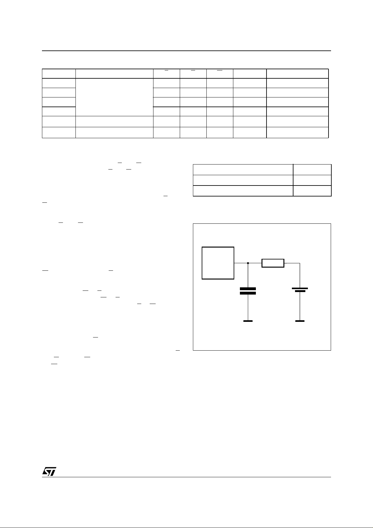
Figure 3. AC Testing Load Circuit
DEVICE
UNDER
TEST
CL includes JIG capacitance
650Ω
CL = 100pF
1.75V
AI01803C
3/14
M48T512Y, M48T512V
Figure 4. Block Diagram
OSCILLATOR AND
CLOCK CHAIN
32,768 Hz
CRYSTAL
POWER
LITHIUM
CELL
VOLTAGE SENSE
AND
SWITCHING
CIRCUITRY
V
CC
DATA RETENTION MODE
With valid V
applied, the M48T512Y/V operates
CC
as a conventional BYTEWIDE™ static RAM.
Should the supply voltage decay, the RAM will automatically deselect, write protecting itself when
V
falls between V
CC
(max), V
PFD
(min) win-
PFD
dow. All outputs become high impedance an d all
inputs are treated as "don't care".
Note: A power fa ilure during a writ e cycle may corrupt data at the current addressed location, but
does not jeopardize the rest of the RAM's content.
At voltage s below V
in a write protected state, provided the V
time is not less than t
spond to transient noise s pi kes on V
(min), the memory will be
PFD
. The M48T512Y/V may re-
F
that cr os s
CC
CC
fall
into the deselect window during the time the device is sampling V
power supply lines is recomm ended. When V
.Therefore, decoupling of the
CC
CC
drops below VSO, the control circuit switches power to the internal battery, preserving data and powering the clock. The internal energy source will
maintain data in the M48T512Y/V for an accumulated period of at least 10 years at room tem perature. As system power rises above V
SO
, the
battery is disconnected, and the power supply is
8 x 8
TIMEKEEPER
REGISTERS
A0-A18
DQ0-DQ7
E
W
G
AI02384
V
PFD
524,280 x 8
SRAM ARRAY
V
SS
switched to external VCC. Write protection continues until V
Normal RAM operation can resume t
exceeds V
reaches V
CC
(max). Refer to Application Note
PFD
(min) plus t
PFD
ER
ER
after V
(AN1012) on the ST Web Site for more information
on battery life.
CLOCK OPERATIONS
Reading the Clock Updates to the TIMEKEEPER
registers should be halted before clock data is
read to prevent reading data in transition. Because
the BiPO RT TIMEKEEPER cells in the R AM array
are only data registers, and not the actual clock
counters, updating the registers can be halted
without disturbing the clock itself. Updating is halted when a '1' is written to t he REA D bi t, D6 i n the
Control Register (7FFF8h). As long as a '1' remains in that position, updat ing is halted. After a
halt is issued, the registers reflect the count; that
is, the day, date, and time that were current at the
moment the halt comm and was issued. All of the
TIMEKEEPER registers are updated simultaneously. A halt will not interrupt an update in
progress. Updating occurs 1 second after the
READ bit is reset to a '0'.
(min).
CC
4/14
M48T512Y, M48T512V
Table 5. Capacitance
(T
= 25 °C, f = 1 MHz)
A
(1)
Symbol Parameter Test Condition Min Max Unit
C
C
IO
Note: 1. Effective capacitance measured with po wer suppl y at 5V (M48T512Y) or 3.3V (M48T512V ). Sampled only, not 100% tested.
2. Outputs desele cted.
Input Capacitance
IN
(2)
Input / Output Capacitance
V
V
OUT
IN
= 0V
= 0V
20 pF
20 pF
Table 6A. DC Characteristics
= 0 to 70 °C; VCC = 4.5V to 5.5V)
(T
A
Symbol Parameter Test Condition Min Max Unit
(1)
I
LI
I
LO
I
CC
I
CC1
I
CC2
V
V
V
V
OH
Note: 1. Outputs deselected.
Input Leakage Current
(1)
Output Leakage Current
Supply Current Outputs open 115 mA
Supply Current (Standby) TTL
Supply Current (Standby) CMOS
Input Low Voltage –0.3 0.8 V
IL
Input High Voltage 2.2
IH
Output Low Voltage
OL
Output High Voltage
0V ≤ V
IN
0V ≤ V
OUT
E
= V
E
= VCC – 0.2V
I
= 2.1mA
OL
I
= –1mA
OH
≤ V
≤ V
IH
CC
CC
±2 µA
±2 µA
8mA
4mA
V
+ 0.3
CC
0.4 V
2.4 V
V
Table 6B. DC Characteristics
= 0 to 70 °C; VCC = 3.0V to 3.6V)
(T
A
Symbol Parameter Test Condition Min Max Unit
(1)
Input Leakage Current
I
LI
(1)
Output Leakage Current
I
LO
I
CC
I
CC1
I
CC2
V
V
V
V
OH
Note: 1. Outputs deselected.
Supply Current Outputs open 60 mA
Supply Current (Standby) TTL
Supply Current (Standby) CMOS
Input Low Voltage –0.3 0.4 V
IL
Input High Voltage 2.2
IH
Output Low Voltage
OL
Output High Voltage
0V ≤ V
IN
0V ≤ V
OUT
E
= V
E
= VCC – 0.2V
I
= 2.1mA
OL
I
= –1mA
OH
≤ V
≤ V
IH
CC
CC
±2 µA
±2 µA
4mA
3mA
V
+ 0.3
CC
0.4 V
2.2 V
V
5/14
 Loading...