

1/4
PRELIMINARY DATA
January 1998
This is preliminary information on a new product now in development or undergoing evaluation. Details are subject to change without notice.
M48T39Y
256 Kb (32K x8) TIMEKEEPER® SRAM
■ INTEGRATED ULTRA LOW POWER SRAM,
REAL TIME CLOCK, POWER-FAIL CONTROL
CIRCUIT, BATTERY and CRYSTAL
■ BCD CODED YEAR, MONTH, DAY, DATE,
HOURS, MINUTES and SECONDS
■ AUTOMATIC POWER-FAIL CHIP DESELECT
and WRITE PROTECTION
■ WRITE PROTECT VOLTAGE
(V
PFD
= Power-fail Deselect Voltage):
– M48T39Y: 4.20V ≤ V
PFD
≤ 4.50V
■ PROGRAMMABLE INTERRUPTS and
SQUARE WAVE OUTPUT
■ WATCHDOG TIMER RESTARTS on
OUT-OF-CONTROL PROCESSOR
■ CLOCK ACCURACY IS BETTER THAN
±1 MINUTE per MONTH at 25°C
■ 10 YEARS of DATA RETENTION and CLOCK
OPERATION in the ABSENCE of POWER
■ SELF-CON TAINED BATTERY and CRYSTA L
in DIP PACKAGE
■ PROG R AMMABLE ALARM OUTPUT ACTIVE
in the BATTERY BACK-UP MODE
■ PIN and FUNCTION COMPATIBLE with
DS1386
DESCRIPTION
The M48T39Y TIMEKEEPER
®
RAM is a non-volatile 262,144 bit static RAM and real time clock organized as 32,768 words by 8 bits. System
integration features include Programmable
Alarms, Watchdog Timer and Interval Timer. The
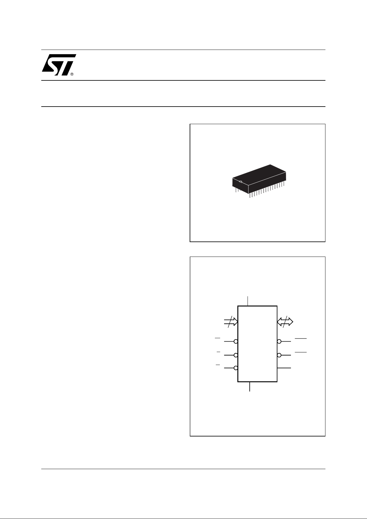
special 32-pin DIP package provides a highly integrated battery back-up memory and real time
clock soluti o n.
Figure 1. Logic Diagram
AI02311
15
A0-A14
W
DQ0-DQ7
V
CC
M48Z129Y
G
V
SS
8
E
INTA
INTB
SQW
32
1
PMDIP32 (PM)
Module
M48T39Y
2/4
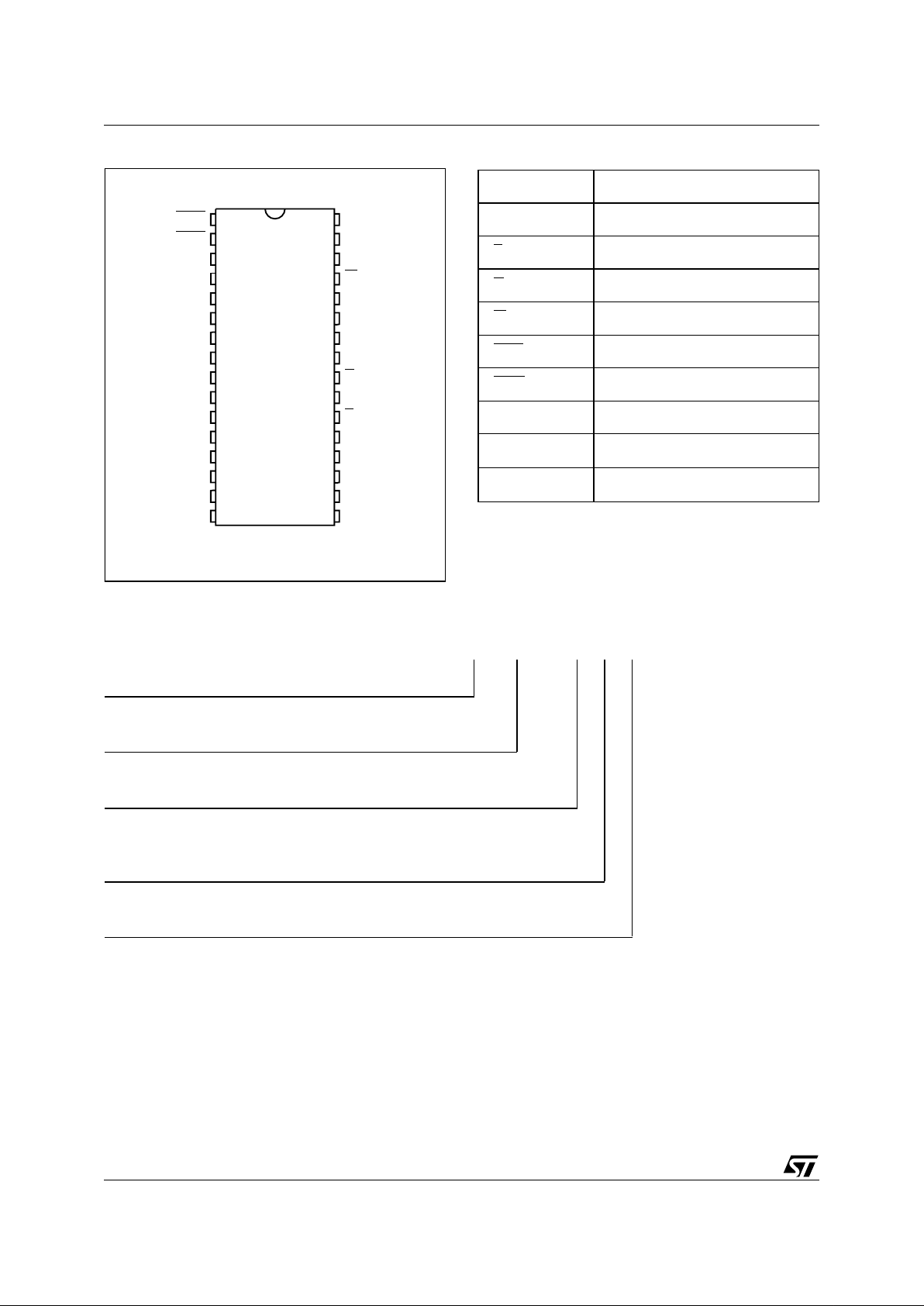
Figure 2. DIP C on ne ctions
A1
A0
DQ0
A7
A4
A3
A2
A6
A5
A13
A10
A8
A9
DQ7
SQW
A11
G
E
DQ5DQ1
DQ2
DQ3V
SS
DQ4
DQ6
INTB
INTA V
CC
AI02312
10
1
2
5
6
7
8
9
11
12
13
14
15
16
30
29
26
25
24
23
22
21
20
19
18
17
A12
A14
W
V
CC
3
4
28
27
32
31
M48T39Y
Table 1. Signal Names
A0-A14 Address Inputs
DQ0-DQ7 Data Inputs / Outputs
E
Chip Enable Input
G
Output Enable Input
W
Write Enable Input
INTA
Interrupt Output A (Open Drain)
INTB
Interrupt Output B (Open Drain)
SQW Square Wave Output
V
CC
Supply Voltage
V
SS
Ground
Table 2. Ordering Information Scheme
For a list of available options (Speed, Pac kage, etc...) or for furthe r information on any aspect of this device, please contact the ST Sales Office nearest to you.
Example: M48T39Y -100 PM 1
Device Type
M48T
Supply Voltage and Write Protect Voltage
39Y = V
CC
= 4.5V to 5.5V; V
PFD
= 4.2V to 4.5V
Speed
-100 = 100ns
-150 = 150ns
Package
PM = PMDIP32
Temperature Range
1 = 0 to 70 °C
 Loading...