

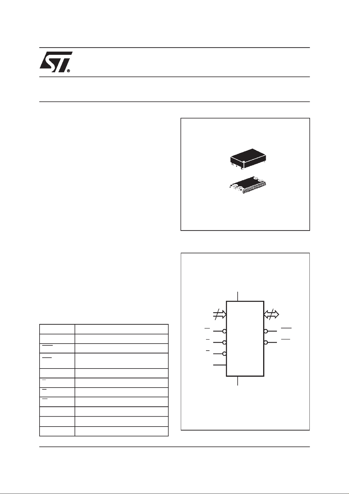
3.3V-5V 256 Kbit (32Kb x8) TIMEKEEPERSRAM
■ INTEGRATED ULTRA-LOW POWER SRAM,
REAL TIMECLOCK, POWER-FAILCONTROL
CIRCUIT and BATTERY
■ FREQUENCY TEST OUTPUT for REAL TIME
CLOCK SOFTWARE CALIBRATION
■ YEAR 2000 COMPLIANT
■ AUTOMATIC POWER-FAIL CHIP DESELECT
and WRITE PROTECTION
■ WATCHDOG TIMER
■ WRITE PROTECT VOLTAGE
(V
= Power-Fail Deselect Voltage):
PFD
– M48T37Y: 4.2V ≤ V
– M48T37V: 2.7V ≤ V
■ PACKAGING INCLUDES a44-LEADSOIC and
SNAPHAT TOP (to be Ordered Separately)
■ SOIC PACKAGE PROVIDES DIRECT
CONNECTION for a SNAPHATTOP which
CONTAINS the BATTERY and CRYSTAL
■ MICROPROCESSOR POWER-ON RESET
(Valid even during battery back-up mode)
■ PROGRAMMABLE ALARM OUTPUT ACTIVE
in the BATTERY BACKED-UP
■ BATTERY LOW FLAG
Table 1. Signal Names
A0-A14 Address Inputs
DQ0-DQ7 Data Inputs / Outputs
RST Power Fail Reset Output (Open Drain)
IRQ/FT
WDI Watchdog Input
E Chip Enable
G Output Enable
W Write Enable
V
CC
V
SS
NC Not connected Internally
Interrupt / Frequency Test Output
(Open Drain)
Supply Voltage
Ground
PFD
PFD
≤ 4.5V
≤ 3.0V
SNAPHAT (SH)
Battery
44
1
SOH44 (MH)
Figure 1. Logic Diagram
V
CC
15
A0-A14
W
E
G
WDI
M48T37Y
M48T37V
V
SS
M48T37Y
M48T37V
8
DQ0-DQ7
RST
IRQ/FT
AI02172
1/20February 2000
M48T37Y, M48T37V
Table 2. Absolute Maximum Ratings
Symbol Parameter Value Unit
T
A
T
STG
(2)
T
SLD
V
IO
V
CC
I
O
P
D
Note: 1. Stresses greater than those listed under ”Absolute Maximum Ratings” may cause permanent damage to the device. This is a stress
rating only and functional operation of the device at these or any other conditions above those indicated in the operational section
of this specification is not implied. Exposure to the absolute maximum rating conditions for extended periods of time may affect
reliability.
2. Soldering temperature not to exceed 260°C for 10 seconds (total thermal budget not to exceed 150°C for longer than 30 seconds).
CAUTION: Negative undershoots below –0.3V are not allowed on any pin while in the Battery Back-up mode.
CAUTION: Do NOT wave solder SOIC to avoid damaging SNAPHATsockets.
Ambient Operating Temperature
Storage Temperature (VCCOff,Oscillator Off)
Lead Solder Temperature for 10 seconds 260 °C
Input or Output Voltages
Supply Voltage
Output Current 10 mA
Power Dissipation 1 W
(1)
Grade 1 0 to 70 °C
Grade 6 –40 to 85 °C
SNAPHAT –40 to 85 °C
SOIC –55 to 125 °C
M48T37Y –0.3 to 7 V
M48T37V –0.3 to 4.6 V
M48T37Y –0.3 to 7 V
M48T37V –0.3 to 4.6 V
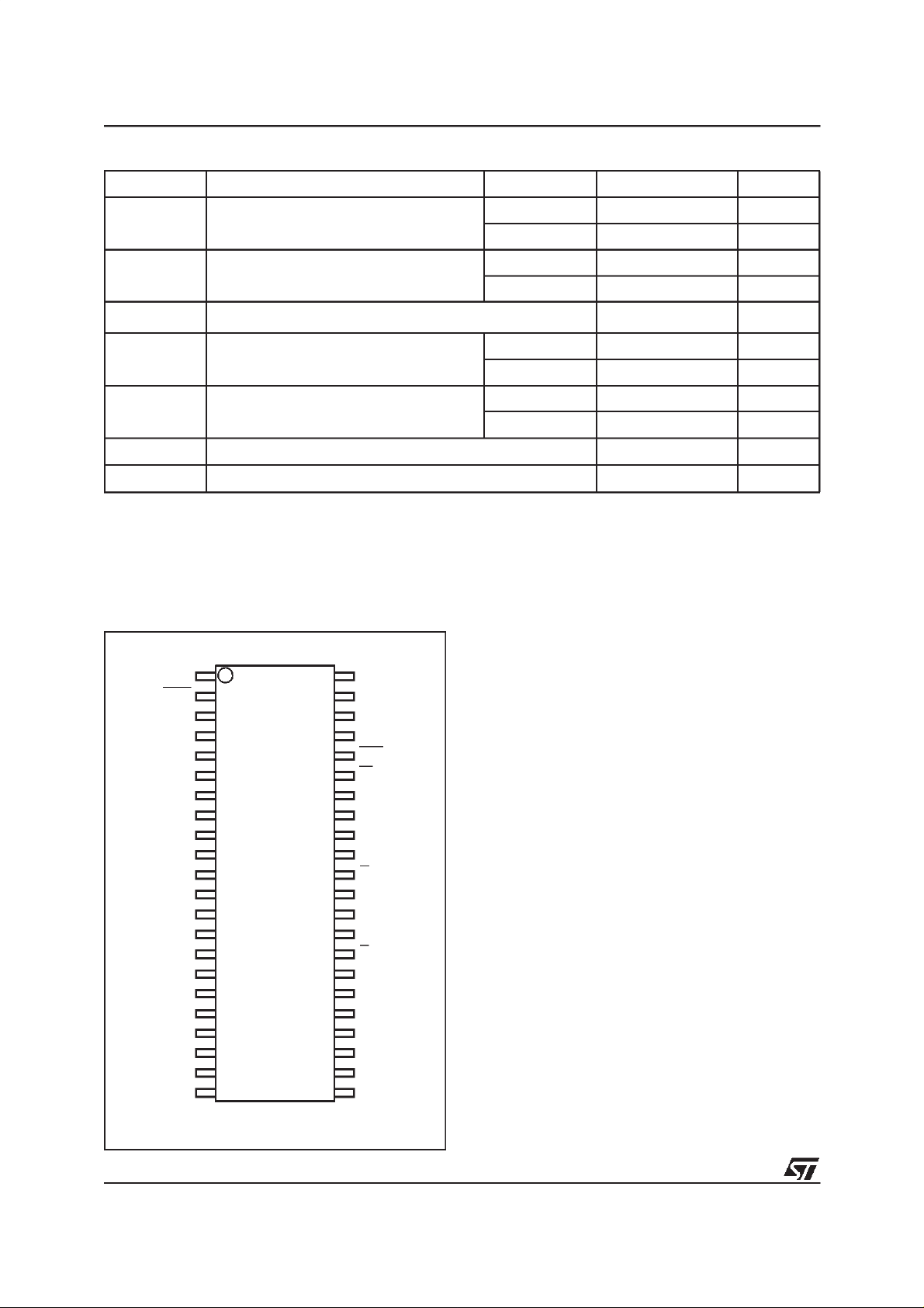
Figure 2. SOIC Connections
NC
RST
NC
NC
A14 IRQ/FT
A12
A7
A6
A5
A4
A3
NC
NC
WDI
A2
A1
A0
DQ0
DQ2
NC
V
SS
1
2
4
5
6
7
8
9
10
11
M48T37Y
M48T37V
12
13
14
15
16
17
18
19
20
21
22
44
43
42
41
40
39
38
37
36
35
34
33
32
31
30
29
28
27
26
25
24
23
AI02174
V
CC
NC
NC3
NC
W
A13
A8
A9
A11
G
NC
NC
A10
E
NC
DQ7
DQ6
DQ5DQ1
DQ4
DQ3
NC
DESCRIPTION
The M48T37Y/37V TIMEKEEPER RAM is a
32Kb x8 non-volatile static RAM and real time
clock. The monolithic chip is available in a special
package which provides a highly integrated battery backed-up memory and real time clock solution.
The 44 lead 330mil SOIC package provides sockets with gold-plated contacts at both ends for direct connection to a separate SNAPHAT housing
containing the battery and crystal. The unique design allows the SNAPHAT battery package to be
mounted on top of the SOIC package after the
completion of the surface mount process.
Insertion of the SNAPHAT housing after reflow
prevents potential battery and crystal damage due
to the high temperatures required for device surface-mounting. The SNAPHAT housing is keyed
to prevent reverse insertion.
The SOIC and battery packages are shipped separately in plastic anti-static tubes or in Tape &Reel
form. For the 44 lead SOIC, the battery/crystal
package (i.e. SNAPHAT) part number is ”M4T28BR12SH” or ”M4T32-BR12SH”.
Caution: Donot place theSNAPHAT battery/crystal topin conductive foam,as this will drain the lithium button-cell battery.
As Figure 3 shows, the static memory array and
the quartz controlled clock oscillator of the
M48T37Y/37V are integrated on one silicon chip.
2/20
M48T37Y, M48T37V
CC
or
PFD
SO
(1)
(min)
(2)
E G W DQ0-DQ7 Power
V
IH
IL
V
IL
V
IL
X X X High Z CMOS Standby
X X X High Z Battery Back-up Mode
Table 3. Operating Modes
Mode V
Deselect
Write V
Read
Read
Deselect
Deselect ≤ V
Note: 1. X = VIHor VIL;VSO= Battery Back-up Switchover Voltage.
2. See Table 7 for details.
4.5V to 5.5V
(M48T37Y)
3.0V to 3.6V
(M48T37V)
to V
V
SO
Figure 3. Block Diagram
IRQ/FT WDI
OSCILLATOR AND
CLOCK CHAIN
32,768
Hz
CRYSTAL
POWER
X X High Z Standby
XVILD
V
IL
V
IH
V
IH
V
IH
16 x 8 BiPORT
SRAM ARRAY
IN
D
OUT
High Z Active
Active
Active
LITHIUM
CELL
VOLTAGE SENSE
AND
SWITCHING
CIRCUITRY
CC
RSTV
V
PFD
32,752 x
SRAM ARRAY
8
V
SS
A0-A14
DQ0-DQ7
E
W
G
AI03253
3/20
M48T37Y, M48T37V
Table 4. AC Measurement Conditions
Input Rise and Fall Times ≤ 5ns
Input Pulse Voltages 0 to 3V
Input and Output Timing Ref. Voltages 1.5V
Note that Output Hi-Z isdefined as the point where data is no longer
driven.
The memory locations, to provide user accessible
BYTEWIDE clock information are in the bytes
with addresses 7FF1 and 7FF9h-7FFFh (located
in Table 11). The clock locations contain the century, year, month, date, day, hour, minute, and
second in 24hour BCD format. Corrections for 28,
29 (leap year-compliant until the year 2100), 30,
and 31 day months are made automatically.
Byte 7FF8h is the clock control register. This byte
controls user access to the clock information and
also stores the clock calibration setting.
Byte 7FF7h contains the watchdog timer setting.
The watchdog timer redirects an out-of-control microprocessor and provides a reset orinterrupt to it.
Byte 7FF2h-7FF5h are reserved for clock alarm
programming.
These bytes can be used to set the alarm. This will
generate an active low signal on the IRQ/FT pin
when the alarm bytes match the date, hours, minutes and seconds of the clock. The eight clock
bytes are not the actual clock counters themselves; theyare memory locations consistingof BiPORT read/write memory cells. The M48T37Y/
37V includes a clock control circuit which updates
the clock bytes with current information once per
second. The information can be accessed by the
user in the same manner as any other location in
the static memory array.
The M48T37Y/37V alsohas its own Power-fail Detect circuit. The control circuitry constantly monitors the single VCCsupply for an out of tolerance
condition. When VCCis out of tolerance, the circuit
writes protects the SRAM, providing a high degree
of data security in the midst of unpredictable system operation broughton by low VCC.AsVCCfalls
below the Battery Back-up Switchover Voltage
(VSO), the control circuitry connects the battery
which maintains data and clock operation until valid power returns.
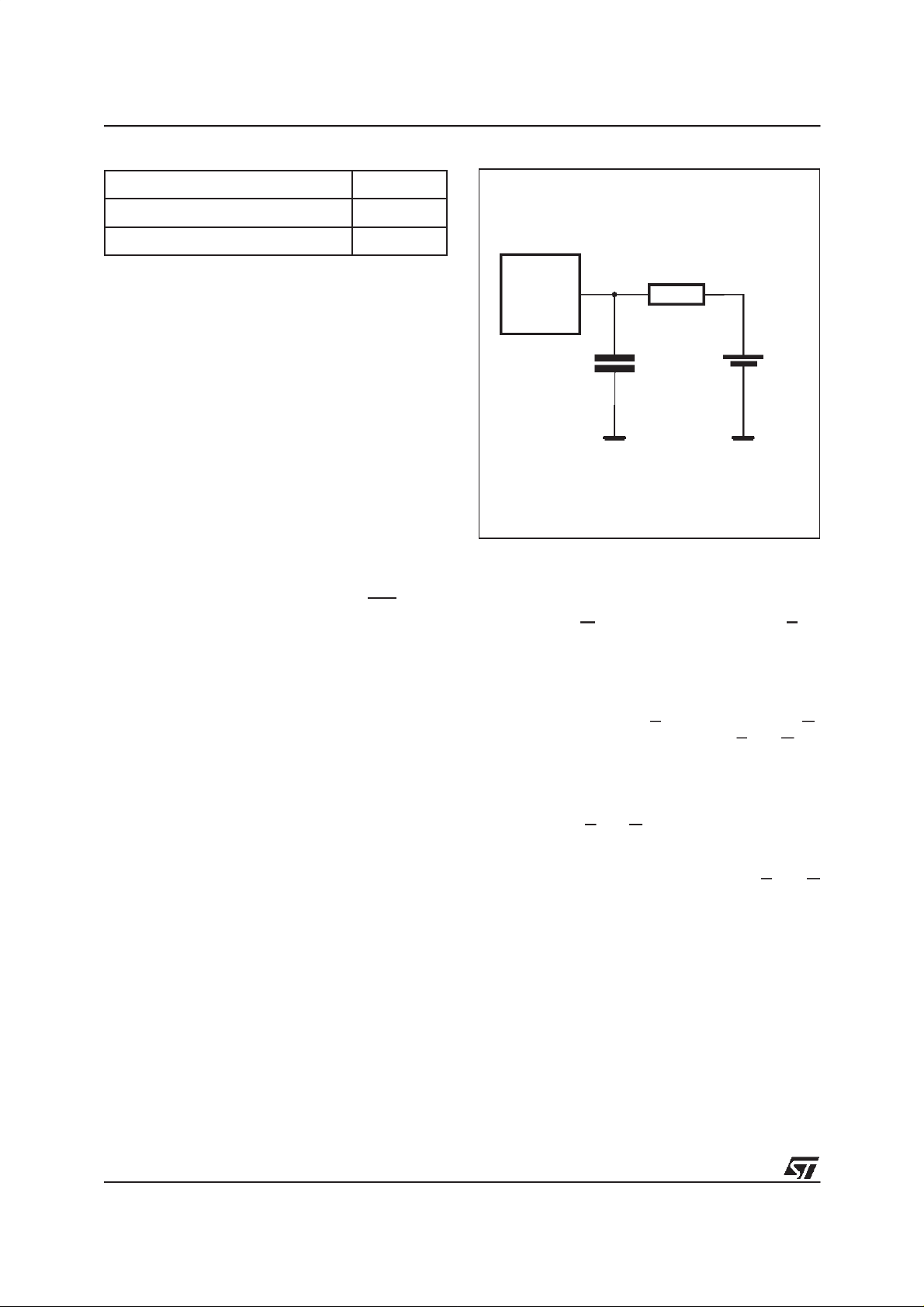
Figure 4. AC Testing Load Circuit
DEVICE
UNDER
TEST
CLincludes JIG capacitance
Note: Excluding open-drain output pins.
645Ω
CL= 100pF
1.75V
AI02325
READ MODE
The M48T37Y/37V is in the Read Mode whenever
Write Enable (W) is high and Chip Enable (E) is
low. The unique address specified by the 15 AddressInputs defineswhich oneof the 32,752 bytes
of data is to be accessed. Valid data will be available at the Data I/O pins within Address Access
time (t
) after the last address input signal is
AVQV
stable, providing that the E and OutputEnable (G)
access times are also satisfied. If the E and G access times are not met, valid data will be available
after the latter of the Chip Enable Access time
(t
) or Output Enable Access time (t
ELQV
GLQV
).
The state of the eight three-state Data I/O signals
is controlled by E andG. If the outputs are activated before t
indeterminate state until t
, the data lineswill be driven to an
AVQV
AVQV
.
If the Address Inputs are changed while E and G
remain active,output data will remainvalid for Output Data Hold time (t
) but will be indetermi-
AXQX
nate until the next Address Access.
4/20
M48T37Y, M48T37V
Table 5. Capacitance
(1, 2)
(TA=25°C)
Symbol Parameter Test Condition Min Max Unit
C
IN
C
IO
Note: 1. Effective capacitance measured with power supply at 5V.
2. Sampled only, not 100% tested.
3. Outputs deselected.
Input Capacitance
(3)
Input / Output Capacitance
V
V
OUT
IN
=0V
=0V
10 pF
10 pF
Table 6. DC Characteristics
(TA= 0 to 70 °C or –40 to 85 °C)
M48T37Y M48T37V
V
Symbol Parameter TestCondition
(1)
I
LI
I
LO
I
I
CC1
I
CC2
V
IL
V
V
V
V
OH
Note: 1. Outputs deselected.
Input Leakage Current
(1)
Output Leakage Current
Supply Current Outputs open 50 33 mA
CC
Supply Current (Standby)
TTL
Supply Current (Standby)
CMOS
(2)
Input Low Voltage –0.3 0.8 –0.3 0.8 V
Input High Voltage 2.2
IH
Output Low Voltage
OL
(standard)
Output Low Voltage
OL
(open drain)
(2)
Output High Voltage IOH= –1mA 2.4 2.4 V
2. Negative spikes of –1V allowed for up to 10ns once per cycle.
0V ≤ V
0V ≤ V
E=V
I
OL
I
OL
IN
OUT
E=V
– 0.2V
CC
= 2.1mA
= 10mA
≤ V
≤ V
IH
CC
CC
= 4.5V to 5.5V VCC= 3.0V to 3.6V
CC
Min Max Min Max
±1 ±1 µA
±1 ±1 µA
32mA
32mA
V
CC
+ 0.3
2.2
VCC+ 0.3
0.4 0.4 V
0.4 0.4 V
Unit
V
5/20
M48T37Y, M48T37V
Table 7. Power Down/Up Trip Points DC Characteristics
(1)
(TA= 0 to 70 °C or –40 to 85 °C)
Symbol Parameter Min Typ Max Unit
M48T37Y 4.2 4.4 4.5 V
V
V
t
Note: 1. All voltages referenced to VSS.
Power-fail Deselect Voltage
PFD
Battery Back-up Switchover Voltage
SO
Expected Data Retention Time (25°C)
DR
2. Using larger M4T32-BR12SH6 SNAPHAT top (recommended for Industrial Temperature Range - grade 6 device).
M48T37V 2.7 2.9 3.0 V
M48T37Y
M48T37V
Grade 1
Grade 6
10
5
(2)
V
BAT
V
–100mV
PFD
7 YEARS
YEARS
Table 8. Power Down/Up AC Characteristics
(TA= 0 to 70 °C or –40 to 85 °C)
Symbol Parameter Min Max Unit
(1)
V
t
F
t
FB
t
R
t
RB
t
REC
Note: 1. V
2. V
3. t
(max) to V
PFD
(2)
V
(min) to VSSVCCFallTime
PFD
V
(min) to V
PFD
VSSto V
(3)
V
(max) to V
PFD
es V
PFD
(min) to VSSfall time of less than tFBmay cause corruption of RAM data.
PFD
(min) = 20ms for Industrial Temperature Range - grade 6 device.
REC
PFD
(max) to RST High
PFD
(min)fall time of less than tF may result in deselection/write protection not occurring until200µs afterVCCpass-
PFD
(min).
(min) VCCFall Time 300 µs
PFD
M48T37Y 10 µs
M48T37V 150 µs
(max) VCCRise Time
PFD
10 µs
(min) VCCRise Time 1 µs
40 200 ms
V
V
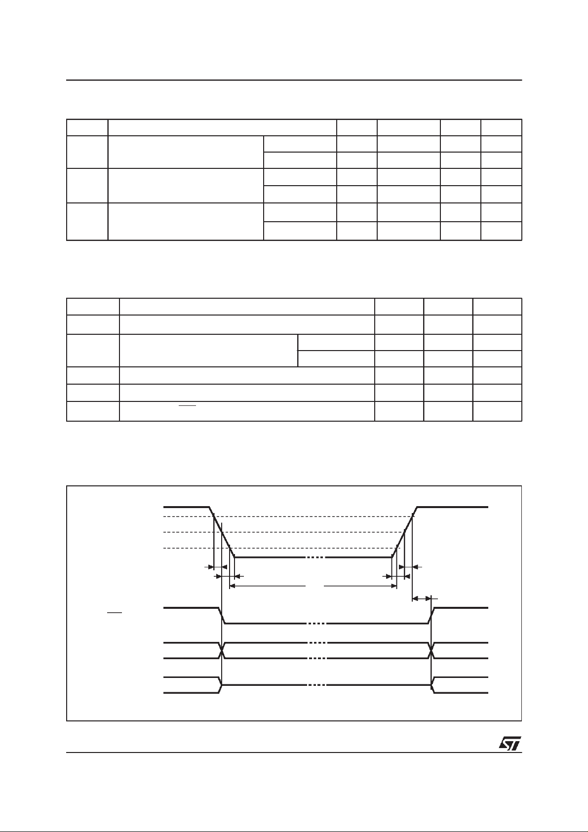
Figure 5. Power Down/Up Mode AC Waveforms
V
CC
V
(max)
PFD
V
(min)
PFD
V
SO
6/20
RST
INPUTS
OUTPUTS
tF
VALID
VALID VALID
tFB
tDR
DON’T CARE
HIGH-Z
tRB
tR
tREC
VALID
AI03078
 Loading...