

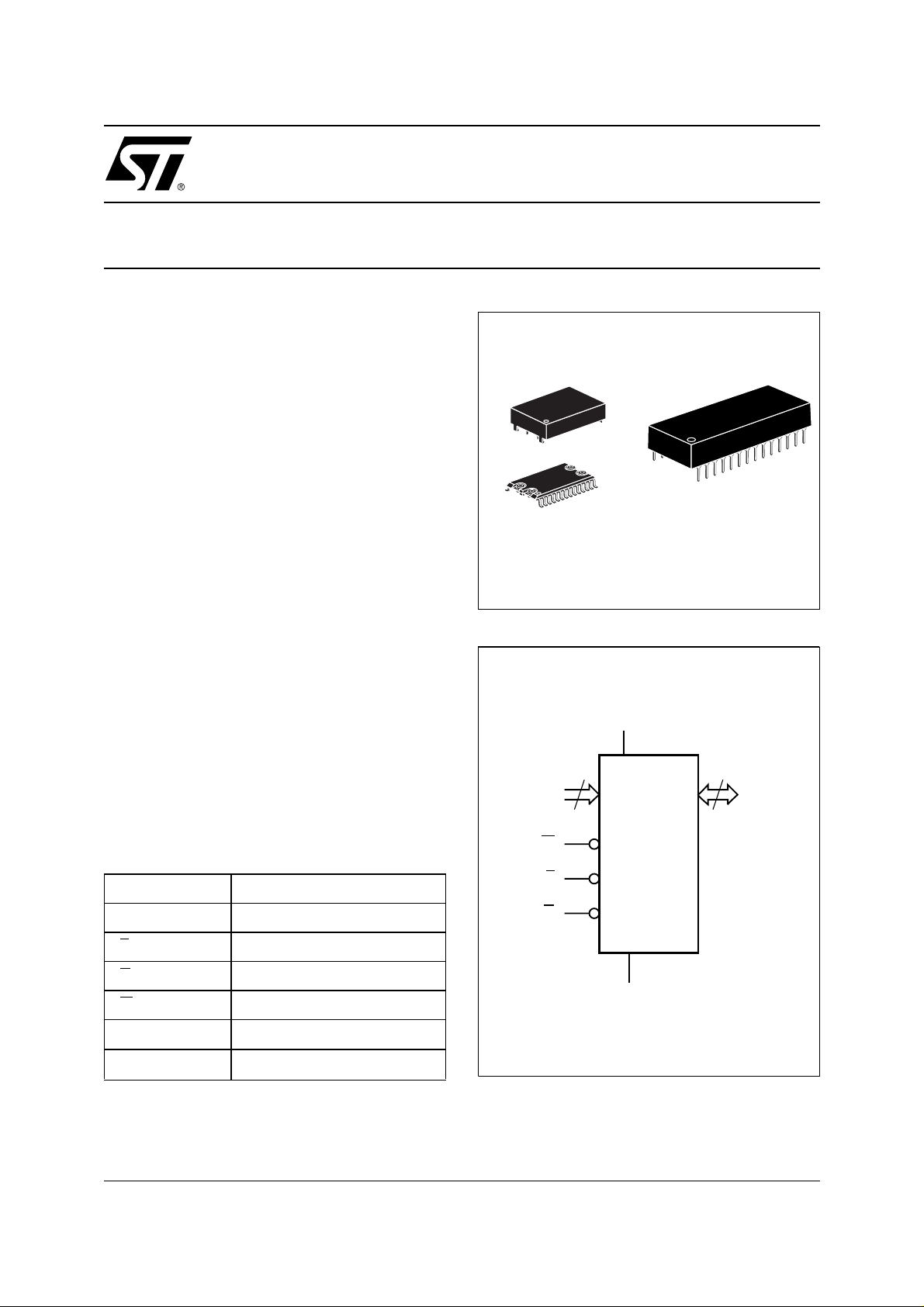
M48T35
M48T35Y
256 Kbit (32Kb x8) TIMEKEEPER® SRAM
■ INTEGRATED ULTRA LOW POWER SRAM,
REAL TIME CLOCK, POWER-FAIL CONTROL
CIRCUIT and BATTERY
■ BYTEWIDE™ RAM-LIKE CLOCK ACCESS
■ BCD CODED YEAR, MONTH, DAY, DATE,
HOURS, MINUTES and SECONDS
■ FREQUENCY TEST OUTPUT for REAL TIME
CLOCK
■ AUTOMATIC POWER-FAIL CHIP DESELECT
and WRITE PROTECTION
■ WRITE PROTECT VOLTAGES
(V
= Power-fail Deselect Voltage):
PFD
– M48T35: 4.5V ≤ V
– M48T35Y: 4.2V ≤ V
■ SELF-CONTAINED BATTERY and CRYSTA L
PFD
PFD
≤ 4.75V
≤ 4.5V
in the CAPHAT DIP PACKAGE
■ SOIC PACKAGE PROVID ES D IREC T
CONNECTION for a SNAPHAT HOUSING
CONTAINING the BATTERY and CRYSTAL
■ SNAPHAT
®
HOUSING (BATTERY and
CRYSTAL) is REPLAC EABLE
■ PIN and FUNCTION COMPATIBLE with
JEDEC STANDARD 32Kb x8 SRAMs
SNAPHAT (SH)
Battery
28
28
1
SOH28 (MH)
Figure 1. Logic Diagram
V
CC
15
A0-A14
1
PCDIP28 (PC)
Battery CAPHAT
8
DQ0-DQ7
Table 1. Signal Names
A0-A14 Address Inputs
DQ0-DQ7 Data Inputs / Outputs
E
G
W
V
V
CC
SS
Chip Enable
Output Enable
Write Enable
Supply Voltage
Ground
W
M48T35
M48T35Y
E
G
V
SS
AI01620B
1/18February 2000
M48T35, M48T35Y
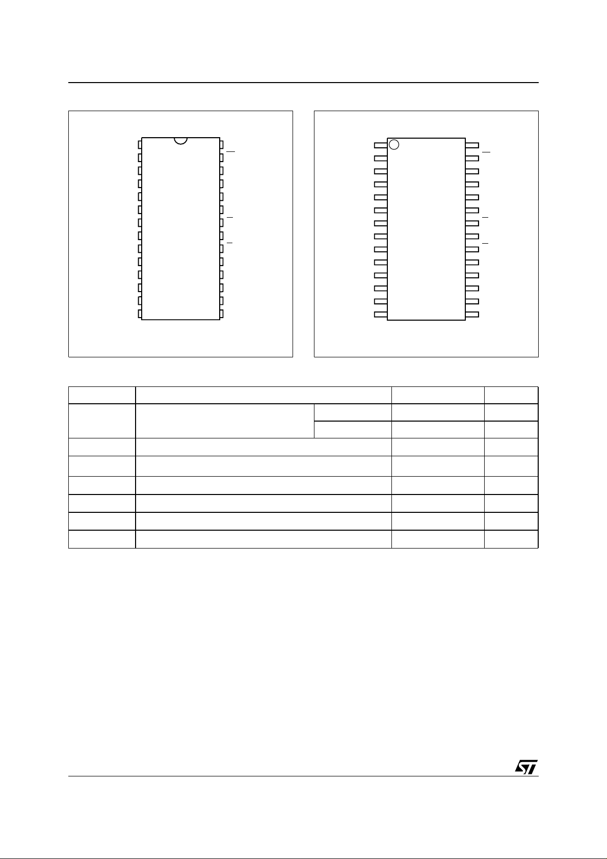
Figure 2A. DIP Connections
A14 V
1
A12
2
3
A7
4
A6
5
A5
6
A4
7
A3
A2
A1
A0
DQ0
8
9
10
11
M48T35
M48T35Y
12
13
DQ2
14
SS
Table 2. Absolute Maximum Ratings
Symbol Parameter Value Unit
T
A
T
STG
(2)
T
SLD
V
IO
V
CC
I
O
P
D
Note: 1. Stresses greater than those listed under "Absolute Maximum Ratings" may cause permanent damage to the device. This is a stress
rating only and functional opera tion of the devi ce at these or any other conditions above those i ndi cated in th e operational section
of this spec ification is not im plied. Exposure t o the abso lute max imum rat ing cond itions for extende d period s of tim e may affe ct
reliability.
2. Soldering temperature not to exceed 260°C for 10 seconds (total thermal budget not to exceed 150°C for longer than 30 seconds).
CAUTION: Negative undershoo ts bel ow –0.3V are not allowed on any pi n while in the B attery Ba ck-up mode.
CAUTION: Do NOT wave solder SOIC to avoid damaging SNAPHAT sockets.
Ambient Operating Temperature
Storage Temperature (VCC Off, Oscillator Off)
Lead Solder Temperature for 10 seconds 260 °C
Input or Output Voltages –0.3 to 7 V
Supply Voltage –0.3 to 7 V
Output Current 20 mA
Power Dissipation 1 W
28
27
26
25
24
23
22
21
20
19
18
17
16
15
AI01621B
CC
W
A13
A8
A9
A11
G
A10
E
DQ7
DQ6
DQ5DQ1
DQ4
DQ3V
(1)
Figure 2B. SOIC Connections
A14 V
A12
A7
A6
A5
A4
A3
A2
A1
A0
DQ0
1
2
3
4
5
6
7
M48T35Y
8
9
10
11
12
DQ2
SS
Grade 1 0 to 70 °C
Grade 6 –40 to 85 °C
13
14
–40 to 85 °C
28
27
26
25
24
23
22
21
20
19
18
17
16
15
AI01622B
CC
W
A13
A8
A9
A11
G
A10
E
DQ7
DQ6
DQ5DQ1
DQ4
DQ3V
DESCRIPTION
®
The M48T35/35Y TIMEKEEPER
RAM is a 32Kb
x8 non-volatile static RAM and real time clock. The
monolithic chip is available in two special packages to provide a highly integrated battery backed-up
memory and real time clock solution.
The M48T35/35Y is a non-volatile pin and function
equivalent to any JEDEC standard 32Kb x8
SRAM. It also easily fits into many ROM, EPROM,
2/18
and EEPROM sockets, providing the non-volatility
of PROMs without any requirement for special
write timing or limitations on the number o f writes
that can be performed.
The 28 pin 600mil DIP CAPHAT houses the
M48T35/35Y silicon with a quartz crystal and a
long life lithium button cell in a single package.
The 28 pin 330mil SOIC provides sockets with
gold plated contacts at both ends for direct con-
M48T35, M48T35Y
V
PFD
≤ V
CC
or
SO
(1)
(min)
(2)
E G W DQ0-DQ7 Power
V
IH
V
IL
V
IL
V
IL
X X X High Z CMOS Standby
X X X High Z Battery Back-up Mode
Table 3. Operating Modes
Mode
Deselect
Write
Read
Read
Deselect
Deselect
Note: 1. X = VIH or VIL; VSO = Battery Back-up Swit ch ov er Volta ge.
2. See T able 7 for deta ils.
4.75V to 5.5V
4.5V to 5.5V
V
to V
SO
Figure 3. Block Diagram
OSCILLATOR AND
CLOCK CHAIN
32,768 Hz
CRYSTAL
X X High Z Standby
X
V
IL
V
IH
V
IL
V
IH
V
IH
8 x 8 BiPORT
SRAM ARRAY
D
D
OUT
IN
Active
Active
High Z Active
A0-A14
POWER
LITHIUM
CELL
VOLTAGE SENSE
AND
SWITCHING
CIRCUITRY
V
CC
nection to a separate SNAPHAT housing cont aining the battery and crystal. The unique design
allows the SNAPHAT battery package to be
mounted on top of the SOIC package after the
completion of the surface mount process. Insertion of the SNAPHAT housing after reflow prevents potential battery and c rystal dam age due to
the high temperatures required for device surfacemounting. The SNAPHAT housing is keyed to prevent reverse insertion. The SOIC and battery/crystal packages are shipped separately in plastic antistatic tubes or in Tape & Reel form.
DQ0-DQ7
E
W
G
AI01623
V
PFD
32,760 x 8
SRAM ARRAY
V
SS
For the 28 lead SOIC, the battery/crystal package
(i.e. SNAPHAT) part number is "M4T28BR12SH1".
As Figure 3 shows, the static memory array and
the quartz controlled clock oscillator of the
M48T35/35Y are integrated on one silicon chip.
The two circuits are interconnected at the upper
eight memory locations to provide user accessible
BYTEWIDE clock information in the bytes with addresses 7FF8h-7FFFh.
3/18
M48T35, M48T35Y
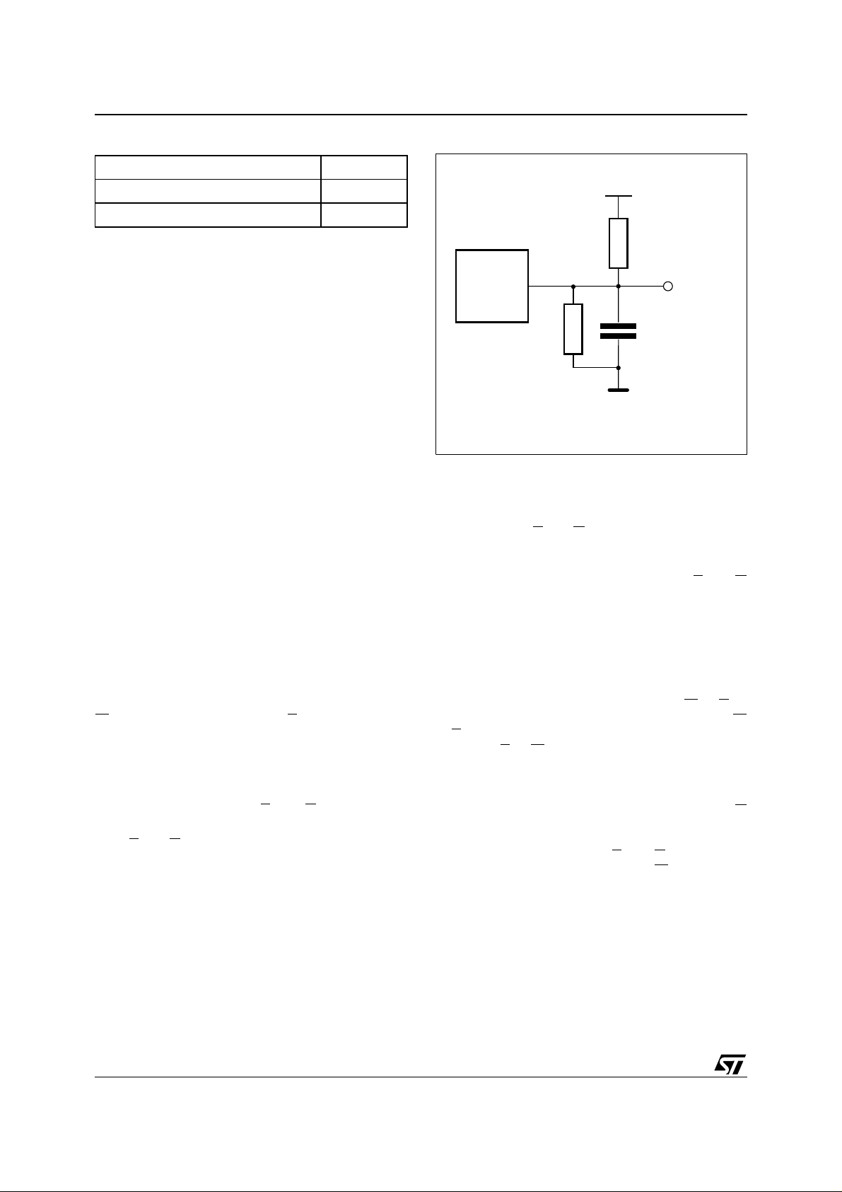
Table 4. AC Measurement Conditions
Input Rise and Fall Times ≤ 5ns
Input Pulse Voltages 0 to 3V
Input and Output Timing Ref. Voltages 1.5V
Note that Output Hi-Z is defined as the point where data is no longer
driven.
The clock locations contain the year, month, date,
day, hour, minute, and second in 24 hour BCD format. Corrections for 28, 29 (leap year), 30, and 31
day months are made automatically. Byte 7FF8h
is the clock control register. This byte controls user
access to the clock information and also stores the
clock calibration setting.
The eight clock bytes are not the actual clock
counters themselves; they are memory locat ions
consisting of BiPORT read/write memory cells.
The M48T35/35Y includes a clock control circuit
which updates the clock bytes with current information once per second. The information can be
accessed by the user i n t he sa me m anner as any
other location in the static memory array.
The M48T35/35Y also has its own Power-fail Detect circuit. The control circuitry constantly monitors the single 5V supply for an out of tolerance
condition. When VCC is out of tolerance, the circuit
write protects the S RAM, p roviding a high degree
of data security in the midst of unpredictable s ystem operation brought on by low V
. As VCC falls
CC
below approximately 3V, the control circuitry connects the battery which maintains data and clock
operation until valid power returns.
READ MODE
The M48T35/35Y is in the Read Mode whenever
(Write Enable) is high and E (Chip Enable) is
W
low. The unique address specified by the 15 A ddress Inputs defines which one of the 32,768 bytes
of data is to be acces sed. Valid data will be available at the Data I/O pi ns within Address Access
time (t
stable, providing that the E
) after the last address input s ignal is
AVQV
and G access times
are also satisfied.
If the E
and G access times are not met, valid data
will be avai la ble af ter the latte r of the C hip Enable
Figure 4. AC Testing Load Circuit
5V
1.9kΩ
DEVICE
UNDER
TEST
1kΩ
CL includes JIG capacitance
Access time (t
(t
).
GLQV
ELQV
) or Output Enable Access time
OUT
CL = 100pF or 5pF
AI01030
The state of the eight t hree-s tate Da ta I/O s i gnals
is controlled by E
ed before t
indeterminate state until t
If the Address Inputs are changed while E
and G. If the outputs are activat-
, the data lines will be driven to an
AVQV
AVQV
.
and G
remain active, output data will remain valid for Output Data Hold time (t
) but will go indetermi-
AXQX
nate until the next Address Access.
WRITE MODE
The M48T35/35Y is in the Write Mode whenever
W and E are low. The start of a write is referenced
from the latter occurring f alling edge of W
or E. A
write is terminated by the earlier rising edge of W
or E. The addresses must be held valid throughout
the cycle. E
of t
EHAX
or W must return high for a minimum
from Chip Enable or t
from Write En-
WHAX
able prior to the initiation of another read or write
cycle. Data -in must be vali d t
of write and remain valid for t
prior to the end
DVWH
afterward. G
WHDX
should be kept high during write cycles to avoid
bus contention; although, if the output bus has
been activated by a low on E
will disab le the ou t pu t s t
and G, a low on W
after W falls.
WLQZ
4/18
M48T35, M48T35Y
Table 5. Capacitance
(T
= 25 °C)
A
(1, 2)
Symbol Parameter Test Condition Min Max Unit
C
IN
C
IO
Note: 1. Effective capacitance measured with power suppl y at 5V.
2. Sampled only, not 100% tested.
3. Outputs desele ct ed.
Input Capacitance
(3)
Input / Output Capacitance
V
V
OUT
IN
= 0V
= 0V
10 pF
10 pF
Table 6. DC Characteristics
(T
= 0 to 70 °C or –40 to 85 °C; VCC = 4.75V to 5.5V or 4.5V to 5.5V)
A
Symbol Parameter Test Condition Min Max Unit
(1)
I
LI
I
LO
I
CC
I
CC1
I
CC2
V
IL
V
IH
V
OL
V
OH
Note: 1. Outputs deselected.
2. Negativ e s p i k e s of –1V allo wed for up t o 10 ns once pe r cycle .
Input Leakage Current
(1)
Output Leakage Current
Supply Current Outputs open 50 mA
Supply Current (Standby) TTL
Supply Current (Standby) CMOS
(2)
Input Low Voltage –0.3 0.8 V
Input High Voltage 2.2
Output Low Voltage
Output High Voltage
0V ≤ V
IN
0V ≤ V
OUT
E
= V
E
= VCC – 0.2V
I
= 2.1mA
OL
I
= –1mA
OH
≤ V
≤ V
IH
CC
CC
±1 µA
±5 µA
3mA
3mA
V
+ 0.3
CC
0.4 V
2.4 V
V
Table 7. Power Down/Up Trip Points DC Characteristics
(1)
(TA = 0 to 70 °C or –40 to 85 °C)
Symbol Parameter Min Typ Max Unit
V
PFD
V
SO
t
DR
Note: 1. All voltages referenced to VSS.
2. CAPHAT and M4T32-BR12SH1 SNAPHAT only, M4T28-BR12SH1 SNAPHAT top t
3. Usi ng larger M4T 32-BR12SH6 SNAPHA T t op (recommended for I ndustrial Temperature Range - grade 6 device).
Power-fail Deselect Voltage
Battery Back-up Switchover Voltage 3.0 V
Expected Data Retention Time
(at 25°C)
M48T35 4.5 4.6 4.75 V
M48T35Y 4.2 4.35 4.5 V
Grade 1
Grade 6
10
10
(2)
(3)
= 7 years (typ) .
DR
YEARS
YEARS
5/18
M48T35, M48T35Y
Table 8. Power Down/Up AC Characteristics
(T
= 0 to 70 °C or –40 to 85 °C)
A
Symbol Parameter Min Max Unit
t
PD
t
F
t
FB
t
R
t
RB
t
REC
Note: 1. V
2. V
3. t
E or W at VIH before Power Down
(1)
V
(max) to V
PFD
(2)
V
(3)
PFD
es V
PFD
PFD
(min) = 20ms for indust ri al temperature grad e (6) device.
REC
(min) to VSS VCC Fall Time
PFD
V
(min) to V
PFD
VSS to V
V
(max) to V
(min).
(min) to VSS fall time of less than tFB may cause corruption of RAM data.
PFD
(max) to Inputs Recognized
PFD
(min) fall time of less than tF may result in deselection/write protection not occurring until 200µs after VCC pass-
PFD
(min) VCC Fall Time
PFD
(max) VCC Rise Time
PFD
(min) VCC Rise Time
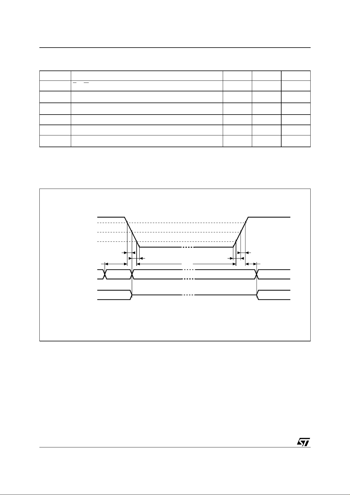
Figure 5. Power Down/Up Mode AC Waveforms
V
CC
V
(max)
PFD
V
(min)
PFD
VSO
tF
tPD
INPUTS
tFB
tDR
tRB
DON'T CARE
0 µs
300 µs
10 µs
10 µs
1µs
40 200 ms
tR
tREC
RECOGNIZEDRECOGNIZED
6/18
OUTPUTS
VALID VALID
(PER CONTROL INPUT)
HIGH-Z
(PER CONTROL INPUT)
AI01168C
 Loading...