

SGS Thomson Microelectronics M48T35AY, M48T35AV Datasheet
M48T35AY
M48T35AV
256 Kbit (32Kb x8) TIMEKEEPER® SRAM
■ INTEGRATED ULTRA LOW POWER SRAM,
REAL TIME CLOCK, POWER-FAIL CONTROL
CIRCUIT and BATTERY
■ BYTEWIDE™ RAM-LIKE CLOCK ACCESS
■ BCD CODED YEAR, MONTH, DAY, DATE,
HOURS, MINUTES and SECONDS
■ BATTERY LOW FLAG (BOK)
■ FREQUENCY TEST OUTPUT for REAL TIME
CLOCK
■ AUTOMATIC POWER-FAIL CHIP DESELECT
and WRITE PROTECTION
■ WRITE PROTECT VOLTAGES
(V
= Power-fail Deselect Voltage):
PFD
– M48T35AY: 4.2V ≤ V
– M48T35AV: 2.7V ≤ V
■ SELF-CO N TAINED BATTERY and CRYSTA L
PFD
PFD
≤ 4.5V
≤ 3.0V
in the CAPHAT DIP PACKAGE
■ SOIC PACKAGE PROVID ES D IREC T
CONNECTION for a SNAPHAT HOUSING
CONTAINING the BATTERY and CRYSTAL
■ SNAPHAT
®
HOUSING (BATTERY and
CRYSTAL) is REPLAC EABLE
■ PIN and FUNCTION COMPATIBLE with
JEDEC STANDARD 32Kb x8 SRAMs
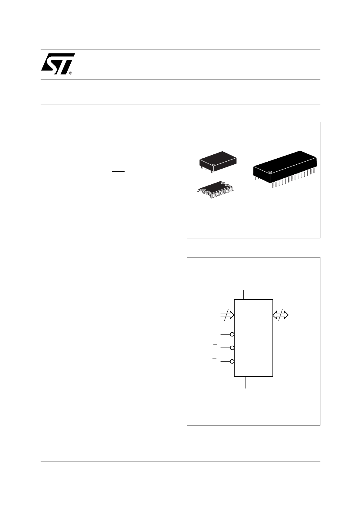
SNAPHAT (SH)
Battery/Crystal
28
28
1
SOH28 (MH)
Figure 1. Logic Diagram
V
CC
15
A0-A14
1
PCDIP28 (PC)
Battery/Crystal
CAPHAT
8
DQ0-DQ7
DESCRIPTION
®
The M48T35AY/35AV TIMEKEEPER
RAM is a
32Kb x8 non-volatile static RAM and real time
clock. The monolithic chip is available in two special packages to provid e a highly integrated battery backed-up memory and real time clock
solution.
The M48T35AY/35AV is a non-volatile pin and
function equivalent to any JEDEC standard 32Kb
x8 SRAM. It also easily fits into many ROM,
EPROM, and EEPROM sockets, providing the
non-volatility of PROMs without any requirement
for special write timing or limitations on the number
of writes that can be performed.
W
M48T35AY
M48T35AV
E
G
V
SS
AI02797B
1/19May 2000
M48T35AY, M48T35AV
Figure 2A. DIP Connections
A14 V
1
A12
2
3
A7
4
A6
5
A5
6
A4
7
A3
A2
A1
A0
DQ0
DQ2
SS
M48T35AY
M48T35AV
8
9
10
11
12
13
14
AI02798B
28
27
26
25
24
23
22
21
20
19
18
17
16
15
CC
W
A13
A8
A9
A11
G
A10
E
DQ7
DQ6
DQ5DQ1
DQ4
DQ3V
Figure 2B. SOIC Connections
A14 V
A12
A7
A6
A5
A4
A3
A2
A1
A0
DQ0
DQ2
SS
1
2
3
4
5
6
7
M48T35AY
M48T35AV
8
9
10
11
12
13
14
AI02799
28
27
26
25
24
23
22
21
20
19
18
17
16
15
CC
W
A13
A8
A9
A11
G
A10
E
DQ7
DQ6
DQ5DQ1
DQ4
DQ3V
Table 1. Signal Names
A0-A14 Address Inputs
DQ0-DQ7 Data Inputs / Outputs
E
G
W
V
V
CC
SS
Chip Enable
Output Enable
Write Enable
Supply Voltage
Ground
The 28 pin 600mil DIP CAPHAT™ houses the
M48T35A Y/ 35A V silicon with a quar tz crys tal a nd
a long life lithium button cell in a single package.
The 28 pin 330mil SOIC provides sockets with
gold plated contacts at both ends for direct connection to a separate SNAPHAT housing cont aining the battery and crystal. The unique design
allows the SNAPHAT battery package to be
mounted on top of the SOIC package after the
completion of the surface mount process. Insertion of the SNAPHAT housing after reflow prevents potential battery and c rystal dam age due to
the high temperatures required for device surfacemounting. The SNAPHAT housing is keyed to prevent reverse insertion.
The SOIC and battery/crystal packages are
shipped separately in plastic anti-static tubes or in
Tape & Reel form.
For the 28 lead SOIC, the battery/crystal package
(i.e. SNAPHAT) part number is "M4T28BR12SH1".
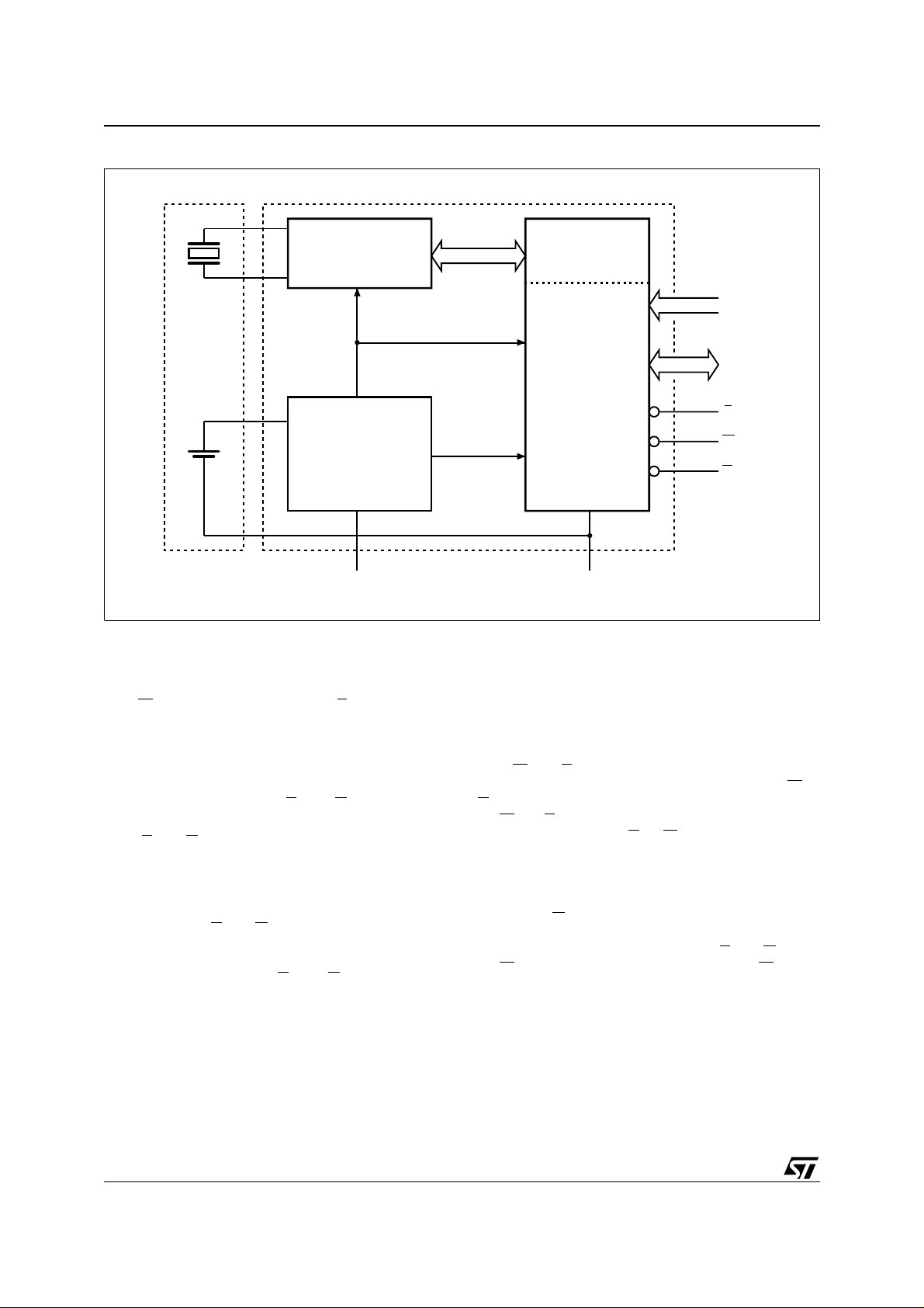
As Figure 3 shows, the static memory array and
the quartz controlled clock oscillator of the
M48T35AY/35AV are integrated on one silicon
chip. The two circuits are interconnected at the upper eight memory locations to provide user acces-
sible BYTEWIDE™ clock i nformation in the bytes
with addresses 7FF8h-7FFFh.
The clock locations contain the year, month, date,
day, hour, minute, and second in 24 hour BCD format. Corrections for 28, 29 (leap year), 30, and 31
day months are made automatically. Byte 7FF8h
is the clock control register. This byte controls user
access to the clock information and also stores the
clock calibration setting.
2/19
M48T35AY, M48T35AV
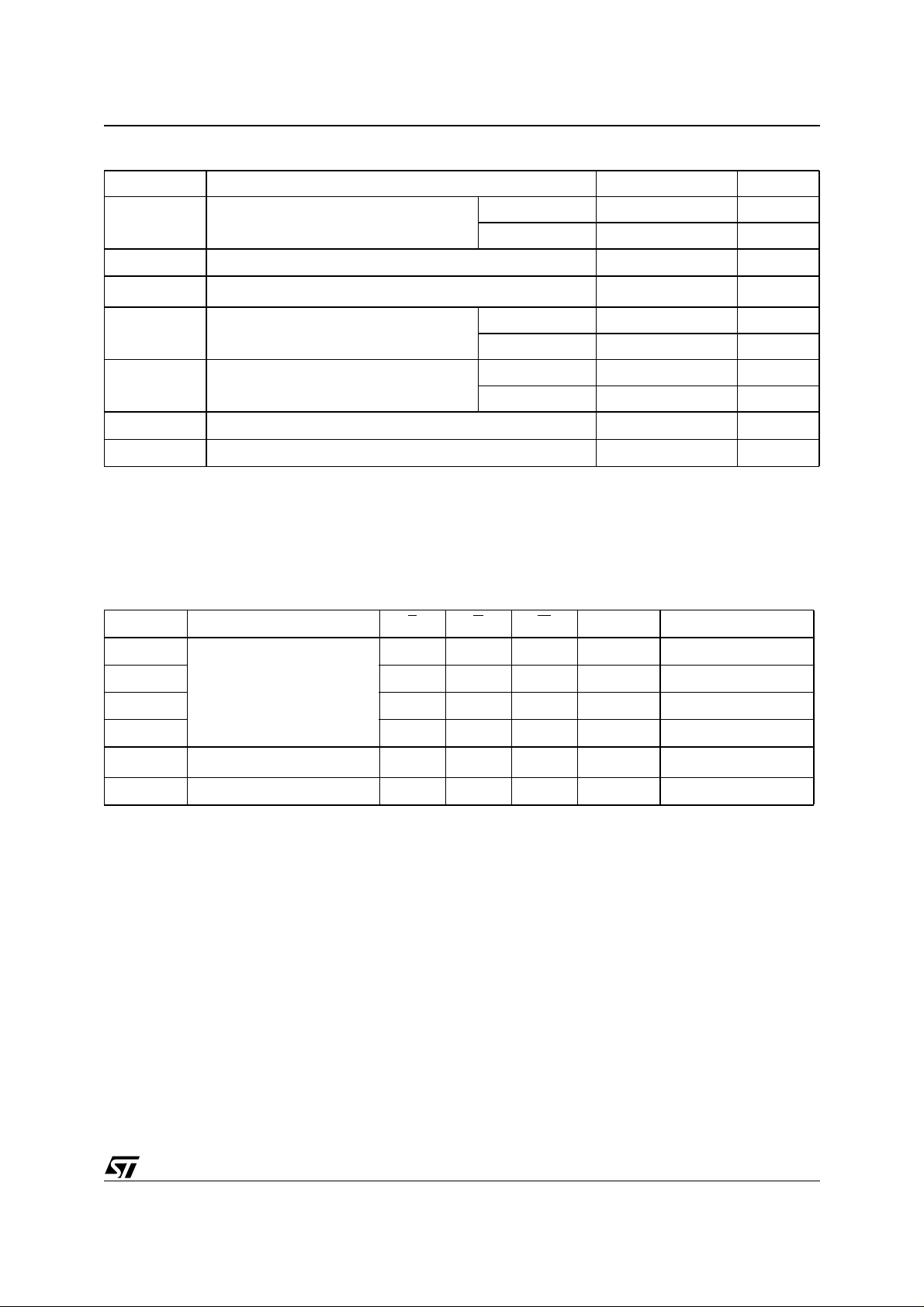
Table 2. Absolute Maximum Ratings
(1)
Symbol Parameter Value Unit
Grade 1 0 to 70 °C
T
T
T
STG
SLD
A
(2)
Ambient Operating Temperature
Grade 6 –40 to 85 °C
Storage Temperature (VCC Off, Oscillator Off)
–40 to 85 °C
Lead Solder Temperature for 10 seconds 260 °C
M48T35AY –0.3 to 7 V
V
IO
Input or Output Voltages
M48T35AV –0.3 to 4.6 V
M48T35AY –0.3 to 7 V
V
CC
I
O
P
D
Note: 1. Stresses greater than those listed under "Absolute Maximum Ratings" may cause permanent damage to the device. This is a stress
rating only and functional opera tion of the devi ce at these or any other conditions above those i ndi cated in th e operational section
of this spec ification is not im plied. Exposure t o the abso lute max imum rat ing cond itions for extende d period s of tim e may affe ct
reliability.
2. Soldering temperature not to exceed 260°C for 10 seconds (total thermal budget not to exceed 150°C for longer than 30 seconds).
CAUTION: Negative undershoo ts bel ow –0.3V are not allowed on any pi n while in the B attery Ba ck-up mode.
Table 3. Operating Modes
Mode
Deselect
Write
Read
Read
Deselect
Deselect
Note: 1. X = VIH or VIL; VSO = Battery Back-up Swit ch ov er Volta ge.
2. See T able 7 for deta ils.
Supply Voltage
M48T35AV –0.3 to 4.6 V
Output Current 20 mA
Power Dissipation 1 W
(1)
4.5V to 5.5V
3.0V to 3.6V
V
to V
SO
≤
V
or
PFD
V
CC
SO
(min)
(2)
E G W DQ0-DQ7 Power
V
IH
V
IL
V
IL
V
IL
X X High Z Standby
X
V
IL
V
IH
V
IL
V
IH
V
IH
D
D
OUT
IN
Active
Active
High Z Active
X X X High Z CMOS Standby
X X X High Z Battery Back-up Mode
The eight clock bytes are not the actual clock
counters themselves; they are memory locat ions
consisting of BiPORT™ read/ write memory cells.
The M48T35AY/35AV includes a clock control circuit which updates the clock bytes with current information once per second. The information can
be accessed by the user in the same manner as
any other location in the static memory array.
The M48T35AY/35AV also has its own Power-fail
Detect circuit. The control circuitry constantly mon-
itors the single 5V supply for an out of tolerance
condition. When V
is out of tolerance, the circuit
CC
write protects the S RAM, p roviding a high degree
of data security in the midst of unpredictable s ystem operation brought on by low V
. As VCC falls
CC
below approximately 3V, the control circuitry connects the battery which maintains data and clock
operation until valid power returns.
3/19
M48T35AY, M48T35AV
Figure 3. Block Diagram
OSCILLATOR AND
CLOCK CHAIN
32,768 Hz
CRYSTAL
POWER
LITHIUM
CELL
VOLTAGE SENSE
AND
SWITCHING
CIRCUITRY
V
CC
READ MODE
The M48T35AY/35AV i s in th e Read M ode whenever W
(Write Enable) is high and E (Chip Enable)
is low. The unique address specified by the 15 Address Inputs defines which one of the 32,768 bytes
of data is to be acces sed. Valid data will be available at the Data I/O pi ns within Address Access
time (t
stable, providing that the E
) after the last address input s ignal is
AVQV
and G access times
are also satisfied.
If the E
and G access times are not met, valid data
will be avai la ble af ter the latte r of the C hip Enable
Access time (t
(t
).
GLQV
) or Output Enable Access time
ELQV
The state of the eight three-s tate Da ta I/O si gnals
is controlled by E
ed before t
indeterminate state until t
puts are changed while E
and G. If the outputs are activat-
, the data lines will be driven to an
AVQV
. If the Address In-
AVQV
and G remain active,
8 x 8 BiPORT
SRAM ARRAY
A0-A14
DQ0-DQ7
E
W
G
AI01623
V
PFD
32,760 x 8
SRAM ARRAY
V
SS
output dat a will rem ain v alid for Outp ut Dat a Hold
time (t
) but will go indeterminate until the next
AXQX
Addr e ss Access.
WRITE MODE
The M48T35AY/35A V is in the Write Mode whenever W
and E are low. The start of a write is referenced from the latter occurring falling edge of W
E
. A write is terminated by the earlier rising edge
of W
or E. The addresses must be held valid
throughout the cycle. E
a minimum of t
EHAX
or W must return high for
from Chip Enable or t
from Write Enable prior to the initiation of another
read or write cycle. Data-in must be valid t
prior to the end of write and remain valid for t
afterward. G should be kept hig h during write cycles to avoid bus contention; although, if the output
after W falls.
WLQZ
and G, a low
bus has been activated by a low on E
on W
will disable the outputs t
or
WHAX
DVWH
WHDX
4/19
M48T35AY, M48T35AV
Table 4. AC Measurement Conditions
Input Rise and Fall Times
Input Pulse Voltages 0 to 3V
Input and Output Timing Ref. Voltages 1.5V
Note that Output Hi-Z is defined as the point where data is no longer
driven.
≤
5ns
DATA RETENTION MODE
With valid V
applied, the M48T35AY/ 35AV op-
CC
erates as a conventional BYT EWIDE stat ic RAM.
Should the supply voltage decay, the RAM will automatically power-fail deselect, write protecting itself when V
falls within the V
CC
(max), VPFD
PFD
(min) window. All outputs become high impedance, and all inputs are treated as "don’t care."
Note: A power failure during a write cycle may corrupt data at the currently addressed location, but
does not jeopardize the rest of the RAM’s content.
At voltages below V
(min), the user can be as-
PFD
sured the memory will be in a write protected state,
provided the V
fall time is not less than tF. The
CC
M48T35AY/35AV may res pond to transient noise
spikes on V
during the time the device is sampling V
that reach into the deselect window
CC
. There-
CC
fore, decoupling of the power supply lines is recommended.
When V
drops below VSO, the control circuit
CC
switches power to the internal battery which preserves data and powers the clock. The internal
button cell will maintain data in the M48T35AY/
35AV for an accumulated period of at least 7 years
when V
turns and V
is less than VSO. As system pow er re-
CC
rises above VSO, the battery is dis-
CC
connected, and the power supply is switched to
external V
reaches V
kept high as V
. Write protection continues until V
CC
(min) plus t
PFD
CC
rises past V
(min). E should be
REC
(min) to prevent
PFD
CC
inadvertent write cycles prior to processor stabilization. Normal RAM operation c an resume t
after VCC exceeds V
Also, as V
rises, the battery voltage is checked.
CC
PFD
(max).
REC
If the voltage is less than approxima tely 2.5V, an
internal Battery Not OK (BOK
BOK
flag can be checked after power up. If the
BOK
flag is set, the first write attempted will be
) flag will be set. The
blocked. The flag is automatically cleared after the
first write, and normal RAM operation resumes.
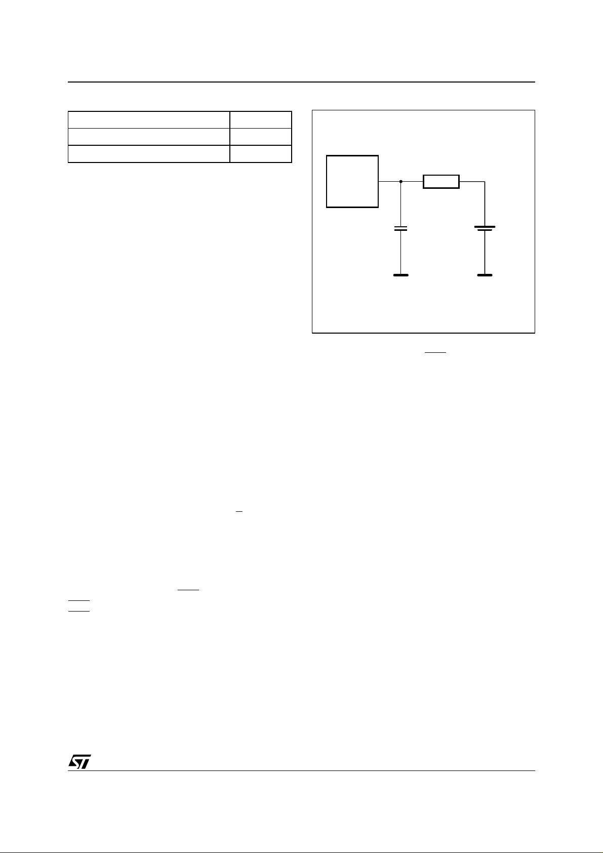
Figure 4. AC Testing Load Circuit
DEVICE
UNDER
TEST
CL includes JIG capacitance
Figure 9 illustrates how a BOK
645Ω
CL = 100pF
(or 5pF)
check routine could
1.75V
AI02586
be structured.
For more information on Battery Storage Life refer
to the Application Note AN1012.
CLOCK OPERATIONS
Reading the Clock
Updates to the TIMEKEEPER registers should be
halted before clock data is read to prevent reading
data in transition. Because the BiPORT TIMEKEEPER cel ls in th e RAM array a re o n ly data re g isters, and not the actual clock counters, updating
the registers can be halted without disturbing the
clock itself.
Updating is halted when a ’1’ is written to the
READ bit, D6 in the Con trol Register 7FF8h. As
long as a ’1’ remains in that position, updating is
halted.
After a halt is issued, the registers reflect the
count; that is, the day, date, and the time that were
current at the moment the halt command was issued.
All of the TIMEKEEPER registers are updated simultaneously. A halt will not interrupt an update in
progress. Updating is within a second after the bit
is reset to a ’0’.
5/19
M48T35AY, M48T35AV
Table 5. Capacitance
(T
= 25°C)
A
(1, 2)
Symbol Parameter Test Condition Min Max Unit
C
IN
C
IO
Note: 1. Effective capacitance measured with power suppl y at 5V.
2. Sampled only, not 100% tested.
3. Outputs desele ct ed.
Input Capacitance
(3)
Input / Output Capacitance
V
V
OUT
IN
= 0V
= 0V
10 pF
10 pF
Table 6A. DC Characteristics
(T
= 0 to 70 °C or –40 to 85 °C; VCC = 4.5V to 5.5V)
A
Symbol Parameter Test Condition Min Max Unit
(1)
I
LI
I
LO
I
CC
I
CC1
I
CC2
V
IL
V
IH
V
OL
V
OH
Note: 1. Outputs deselected.
2. Negativ e s p i k e s of –1V allo wed for up t o 10 ns once pe r Cycle.
Input Leakage Current
(1)
Output Leakage Current
Supply Current Outputs open 50 mA
Supply Current (Standby) TTL
Supply Current (Standby) CMOS
(2)
Input Low Voltage –0.3 0.8 V
Input High Voltage 2.2
Output Low Voltage
Output High Voltage
0V ≤ V
IN
0V ≤ V
OUT
E
= V
E
= VCC – 0.2V
I
= 2.1mA
OL
I
= –1mA
OH
≤ V
≤ V
IH
CC
CC
±1 µA
±5 µA
3mA
3mA
V
+ 0.3
CC
0.4 V
2.4 V
V
Table 6B. DC Characteristics
(T
= 0 to 70 °C or –40 to 85 °C; VCC = 3.0V to 3.6V)
A
Symbol Parameter Test Condition Min Max Unit
(1)
I
LI
I
LO
I
CC
I
CC1
I
CC2
V
IL
V
IH
V
OL
V
OH
Note: 1. Outputs deselected.
2. Negativ e s p i k e s of –1V allo wed for up t o 10 ns once pe r Cycle.
Input Leakage Current
(1)
Output Leakage Current
Supply Current Outputs open 30 mA
Supply Current (Standby) TTL
Supply Current (Standby) CMOS
(2)
Input Low Voltage –0.3 0.8 V
Input High Voltage 2.2
Output Low Voltage
Output High Voltage
0V ≤ V
IN
0V ≤ V
OUT
E
= V
E
= VCC – 0.2V
I
= 2.1mA
OL
I
= –1mA
OH
≤ V
≤ V
IH
CC
CC
±1 µA
±5 µA
2mA
2mA
V
+ 0.3
CC
0.4 V
2.4 V
V
6/19
 Loading...