

SGS Thomson Microelectronics LM2902, LM2902N, LM2902D Datasheet
LOW POWER QUAD OPERATIONAL AMPLIFIERS
.WIDEGAINBANDWIDTH : 1.3MHz
.INPUTCOMMON-MODE VOLTAGERANGE
INCLUDES GROUND
.LARGEVOLTAGE GAIN : 100dB
.VERYLOWSUPPLYCURRENT/AMPLI: 375µA
.LOW INPUT BIAS CURRENT : 20nA
.LOW INPUT OFFSETCURRENT : 2nA
.WIDEPOWERSUPPLYRANGE:
SINGLESUPPLY: +3V TO +30V
DUALSUPPLIES: ±1.5VTO ±15V
DESC RIP TI ON
This circuit consistsof four independent,highgain,
internallyfrequency compensatedoperational amplifiers whichwere designedspecificallyforautomotive andindustrialcontrolsystems. It operatesfrom
a single power supply over a wide range of voltages. Operation from split power supplies is also
possibleand the low power supply currentdrain is
independentof the magnitude of the power supply
voltage.
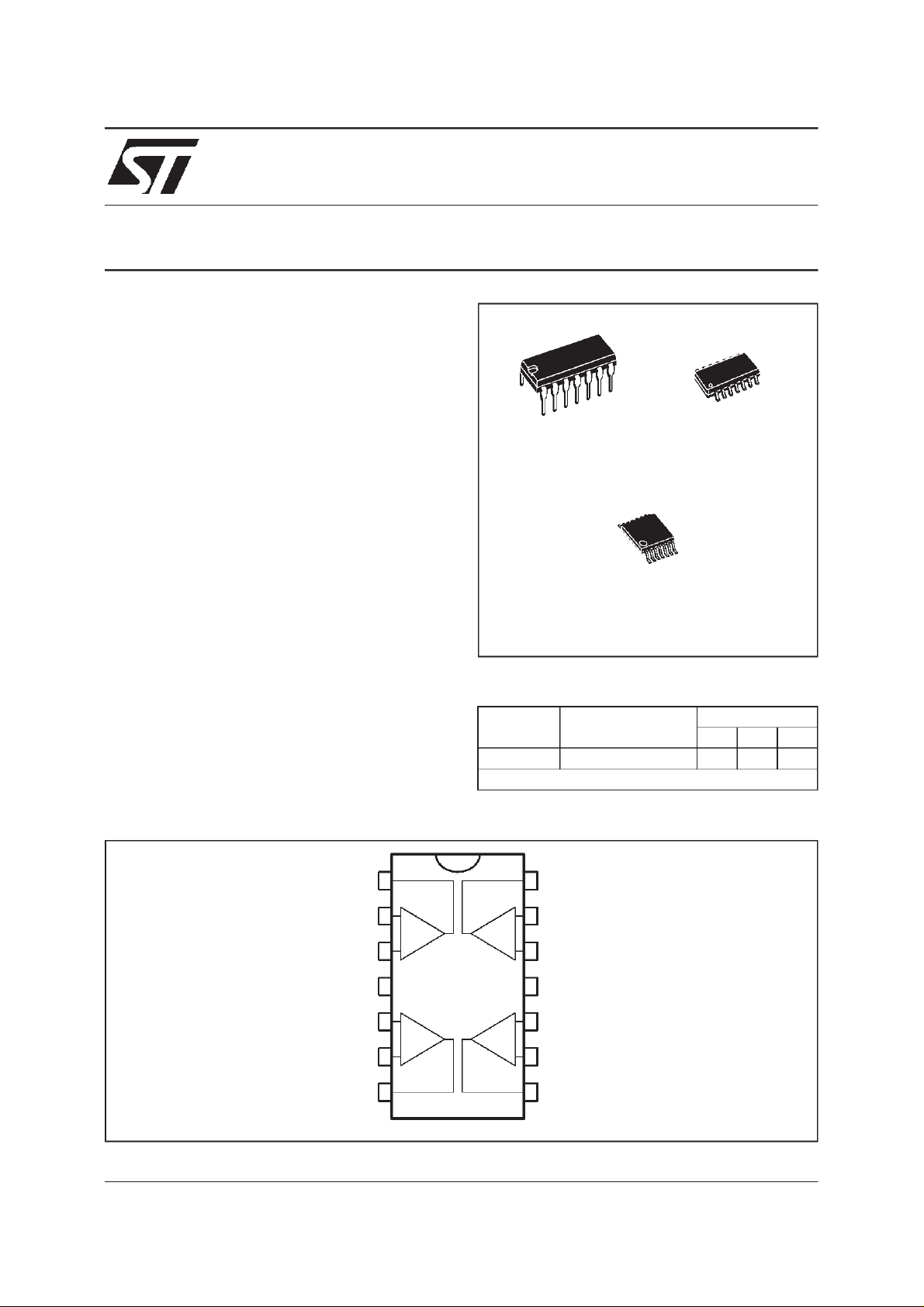
N
DIP14
(PlasticPackage)
(Thin Shrink Small Outline Package)
ORDER CODES
Part
Number
LM2902 -40
Example : LM2902D
LM290 2
D
SO14
(PlasticMicropackage)
P
TSSOP14
Temperature
Range
o
C, +125oC •••
Package
NDP
PI N CONNECT I O NS ( top view)
Output 1
Inverting Input 1
Non-inverting Input 1
V
CC
Non-inverting Input 2
Inverting Input 2
Output 2
August 1998
1
2
3
+
4
5
6
7
-
+
+
-
14
Output 4
13
-
+
+
-
Inverting Input 4
12
Non-inverting Input 4
11
10
9
8
-
CCV
Non-inverting Input 3
Inverting Input 3
Output 3
1/14
LM2902
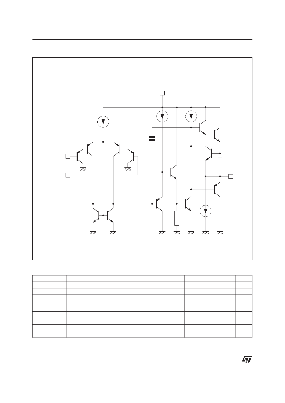
SCHE MATIC DI AG RAM (1/4 L M2902)
V
CC
Inverting
input
Non-inve rting
input
6µA
Q2
Q3
Q8 Q9
4µA
100µA
Q5
C
C
Q4Q1
Q7
Q11
Q6
R
SC
Output
Q13
Q10
Q12
50µA
GND
ABSOLUTE MAXIMUM RATINGS
Symbol Parameter LM2902 Unit
2/14
V
cc
V
i
V
id
P
tot
- Output Short-circuit Duration - (note 1) Infinite
I
in
T
oper
T
stg
Supply Voltage ±16 or 32 V
Input Voltage -0.3 to +32 V
Differential Input Voltage +32 V
Power Dissipation N Suffix
D Suffix
500
400
Input Current – (note 6) 50 mA
Operating Free Air Temperature Range -40 to +125
Storage Temperature Range -65 to +150
mW
mW
o
C
o
C

ELECTRICAL CHARACTERISTICS
V
CC
+
= +5V, V
–
= Ground, VO= 1.4V, T
CC
amb
= +25oC
(unless otherwise specified)
Symbol Parameter Min. Typ. Max. Unit
V
io
I
io
I
ib
A
vd
SVR Supply Voltage Rejection Ratio (R
I
CC
V
icm
CMR Common-mode Rejection Ratio (R
I
o
I
sink
Input Offset Voltage (note 3)
=+25oC
T
amb
≤ T
≤ T
T
min.
amb
max
.
Input Offset Current
=+25oC
T
amb
≤ T
≤ T
T
min.
amb
max
.
Input Bias Current (note 2)
=+25oC
T
amb
≤ T
≤ T
≤ T
≤ T
max
max
max
.
.
≤ 10kΩ)
S
.
T
min.
amb
Large Signal Voltage Gain
+
= +15V, RL=2kΩ,VO= 1.4V to 11.4V)
(V
CC
=+25oC
T
amb
≤ T
T
min.
amb
+
= 5V to 30V)
(V
CC
=+25oC
T
amb
≤ T
T
min.
amb
Supply Current, all Amp, no load
=+25oCV
T
amb
≤ T
≤ T
T
min.
amb
.VCC= +5V
max
V
V
CC
CC
CC
= +5V
= +30V
= +30V
Input Common Mode Voltage Range
= +30V) - (note 4)
(V
CC
=+25oC
T
amb
≤ T
T
T
T
min.
amb
min.
amb
=+25oC
≤ T
amb
≤ T
≤ T
max.
max
≤ 10kΩ)
S
Output Short-circuit Current (Vid= +1V)
= +15V, Vo= +2V 20 40 70
V
CC
Output Sink Current (Vid= -1V)
= +15V, Vo=+2V
V
CC
= +15V, Vo= +0.2V
V
CC
50
25
65
65
70
60
10
12
27
9
230
40
20 150
300
100
110
0.7
1.5
0.8
1.5
0
0
1.2
3
1.2
3
VCC-1.5
-2
V
CC
80
20
50
LM2902
mV
nA
nA
V/mV
dB
mA
V
dB
mA
mA
µA
3/14
LM2902
ELECTRICAL CHARACTERISTICS (continued)
Symbol Parameter Min. Typ. Max. Unit
V
OH
V
OL
SR Slew Rate (V
GBP Gain Bandwidth Product (V
THD Total Harmonic Distortion
e
n
DV
DI
IO
1/VO2 Channel Separation (note 5)
V
O
Notes : 1. Short-circuits from the output to VCCcan cause excessive heati ng if VCC> 15V. The maximum output current
High Level Output Voltage
= +30V)
(V
CC
= +25oCR
T
amb
. ≤ T
T
min
= +25oCR
T
amb
. ≤ T
T
min
= +5V, RL=2kΩ)
(V
CC
= +25oC
T
amb
. ≤ T
T
min
amb
amb
amb
≤ T
≤ T
≤ T
max
max
max
.
.
.
=2kΩ
L
= 10kΩ
L
Low Level Output Voltage (RL= 10kΩ)
= +25oC
T
amb
. ≤ T
T
min
=2kΩ,CL= 100pF, unity gain) 0.4
R
L
f = 100kHz, V
(f = 1kHz, A
CL= 100pF, VCC= 30V) 0.015
≤ T
amb
CC
in
= 20dB, RL=2kΩ,VO=2V
V
.
max
= 15V, VI= 0.5 to 3V,
= 30V
= 10mV, RL=2kΩ,CL= 100pF) 1.3
CC
pp
26
26
27
27
3.5
3
27
28
mV
520
20
V/µs
MHz
Equivalent Input Noise Voltage
(f = 1kHz, R
Input Offset Voltage Drift 7 30 µV/oC
io
= 100Ω,VCC= 30V) 40
s
√Hz
Input Offset Current Drift 10 200 pA/oC
1kHz ≤ f ≤ 20kHz 120
is approximately 40mA i ndependent of the m agnitude of V
neous short-circuit on all amplifiers.
2. The dir ection of the input current is out of the IC . This current is essentially constant, independent of the state
of the output so no loading change exists on the i nput l ines.
= 1.4V, Rs=0Ω, 5V < V
3. V
o
4. The input common-mode voltage of either input signal voltage should not be allowed to go negative by more
than 0.3V. The upper end of the common-mode voltage range i s V
to + 32V wi thout damage.
5. Due t o the proximity of external components insure that coupling is not originating via stray capacitance between these ext ernal parts. This typically can be detected as this t ype of capacitance increases at higher frequen ces.
6. This input current only exists when the voltage at any of t he i nput leads is driven negative. It is due to the
collector-base junction of the input PN P transistor becoming forward biased and thereby acting as input diodes clamps. I n addition to this diode action, there is also NPN parasitic act ion on the IC chip. t his t ransistor
act ion can cause the out put voltag es of th e Op-amps to go to t he V
overdrive) for the time duration than an input i s dr iven negative.
This i s not destructive and normal output wi ll set up again f or input voltage higher than -0.3V.
+
<30V,0<Vic<V
CC
CC
+
. Des t ru ctive dissipation can r esul t fro m sim ulta-
CC
-1.5V
+
- 1.5V, but either or both inputs can go
CC
voltage l evel (or to ground for a large
CC
V
%
nV
dB
4/14

LM2902
IB (nA)
INPUT BIAS CURRENT
versus AMBIENT TEMPERATURE
24
21
18
15
12
9
6
3
0
-55-35-15 5 25 45 65 85 105 125
AMBIENT TEMPERATURE
INPUT VOLTAGE RANGE
15
10
5
INPUT VOLTAGE (V)
0 5 10 15
NØgative
Positive
POWER SUPPLY VOLTAGE (–V)
CURRENT LIMITING (Note 1)
90
80
70
60
50
40
30
20
OUTPUT CURRENT (mA)
10
0
-55 -35 -15 5 25 45 65 85 105 125
(
C)
TEMPERATURE( C)
-
+
I
O
SUPPLYCURRENT
4
V
CC
I
mA
3
2
1
D
-
+
T
=0 C to +125 C
amb
SUPPLY CURRENT (mA)
T
=-55 C
amb
0102030
POS ITIVE SUPP LYVOLTAGE (V)
GBP (mhz)
1.35
1.30
1.25
1.2
1.15
1.1
1.05
-95
-9
GAIN BANDWIDTH PRODUCT (MHz)
GAIN BANDWIDTH PRODUCT
1
-55-35-15 5 25 45 6 5 85 105 12 5
(
AMBIENT TEMPERATURE
C)
COMMON MODE REJECTION RATIO
120
100
80
60
40
20
0
COMMON MODE REJECTION RATIO (dB)
100 1K
e
I
100k
+7.5V
Ω
100
-
Ω
100
+
Ω
+7.5V
10K 100K
FREQUENCY (Hz)
100kΩ
e
O
1M
5/14
 Loading...