

LOWPOWER QUAD VOLTAGE COMPARATORS
.WIDESINGLESUPPLYVOLTAGERANGEOR
DUAL SUPPLIES FOR ALL DEVICES: +2V TO
+36V OR ±1V TO ±18V
.VERYLOWSUPPLYCURRENT(1.1mA) IN-
DEPENDENT OF SUPPLY VOLTAGE
(1.4mW/comparatorat +5V)
.LOW INPUT BIAS CURRENT: 25nA TYP
.LOW INPUT OFFSET CURRENT : ±5nA TYP
.INPUT COMMON-MODE VOLTAGE RANGE
INCLUDES GROUND
.LOW OUTPUT SATURATION VOLTAGE :
250mV TYP. (IO= 4mA)
.DIFFERENTIAL INPUT VOLTAGE RANGE
EQUALTO THE SUPPLY VOLTAGE
.TTL, DTL, ECL, MOS, CMOS COMPATIBLE
OUTPUTS
N
DIP14
(PlasticPackage)
LM2901
D
SO14
(PlasticMicropackage)
DESCRI PT ION
This device consists of four independent precision
voltage comparators. All these comparators were
designedspecificallytooperatefroma singlepower
supply over a wide range of voltages. Operation
fromsplit power supplies is also possible.
These comparators also have a unique
characteris-tic in that the input common-mode voltage range includes ground even though operated
froma singlepower supply voltage.
PIN CONNECTIONS (top view)
Output 2
Output 1
Inverting input 1
Non-inve rting input 1
Inverting input 2
Non-inve rting input 2
1
2
V
+
3
CC
4
5
6
7
TSSOP14
(Thin Shrink Small OutlinePackage)
ORDER CODES
Part
Number
LM2901 -40, +125
Example : LM2901D
14
Output 3
13
Output 4
12
V
CC
11
Non-inve rting input 4
10
Inverting input 4
9
Non-inve rting input 3
8
Inverting input 3
Temperature
Range
-
P
Package
o
C
NDP
•••
December1999
1/10
LM2901
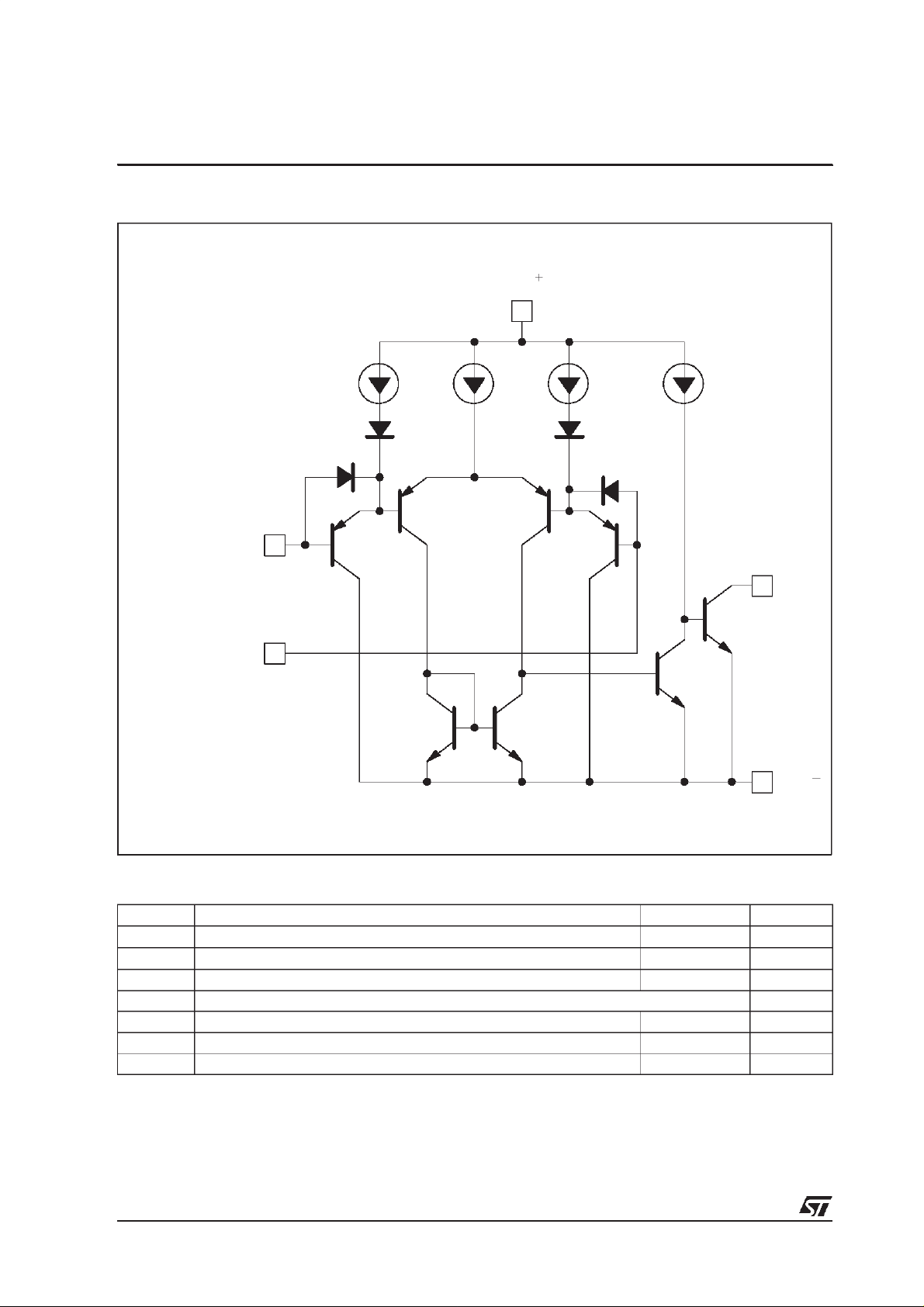
SCHEMA TI C DIAGRAM ( 1/4 LM2901)
V
CC
Non-inverting
Input
Inverting
Input
µ
A 100µA3.5
3.5
µ
A 100µA
V
V
O
CC
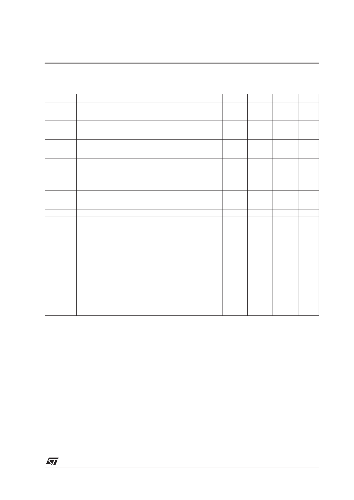
ABSOLUTE MAXIMUM RATINGS
Symbol Parameter LM2901 Unit
V
V
V
P
T
oper
T
Notes : 1. Short-circuit f rom the output t o V
2/10
Supply Voltage
CC
Differential Input Voltage
id
Input Voltage -0.3 to +36 V
I
Output Short-circuit to Ground - note 1
Power Dissipation 570 mW
tot
Operating Free-air Temperature Range -40, +125
Storage Temperature Range -65, +150
stg
output current is approximately 20mA, i ndependent of the magnitude of V
+
can cause excessive heating and eventual destruction. The maximum
CC
CC
+
.
±18 to 36
±36
V
V
o
C
o
C
LM2901
ELECTRICAL CHARACTERISTICS
+
V
= +5V, V
CC
Symbol Parameter Min. Typ. Max. Unit
V
io
I
io
I
ib
A
vd
I
CC
V
icm
V
id
V
OL
I
OH
I
sink
t
re
t
rel
Notes : 2.
At output sw itch point, VO≈ 1.4V , RS=0withV
range (0V to V
3. T he direction of the i nput current i s out of the IC due to the PNP i nput stage. This current is essentially
constant, independent of the state of the output, so no loading charge exists on the reference of i nput
lines.
4. T he input common-mode voltage of either input signal voltage should not be allowed to go negative by
more than 0.3V. The upper end of t he common-mode volt age range is V
can go to +30V without damage.
5. T he response time specifi ed is for a 100mV input step wi th 5mV overdrive.
6. P ositi ve excursions of i nput voltage may exceed the power supply level. As long as the other v oltage remains within the common-mode range, the comparator wi l l provide a proper output state. The low i nput
voltage state m ust not be less than –0.3V (or 0.3V bellow t he negative power supply, if used).
7. M aximum values are guaranteed by design.
-
= GND, T
CC
=25oC (unless otherwise specified)
amb
Input Offset Voltage - note 2
T
T
amb
min.
= +25oC
≤ T
amb
≤ T
max.
17
Input Offset Current
T
= +25oC
amb
T
≤ T
amb
≤ T
min.
Input Bias Current (I
T
= +25oC
amb
≤ T
T
min.
amb
≤ T
max.
+
I
max.
or I
–
) - note 3
I
550
25 250
Large Signal Voltage Gain
= 15V, RL=15kΩ,VO= 1 to 11V)
(V
CC
25 200
Supply Current (all comparators)
V
= +5V, no load
CC
V
= +30V, no load
CC
1.1
1.3
Input Common Mode Voltage Range (VCC= 30V) - note 4
T
T
amb
min
= +25oC
. ≤ T
amb
≤ T
max.
0
0
V
V
Differential Input Voltage - note 6 V
Low Level Output Voltage
(V
T
T
id
amb
min.
= -1V, I
= +25oC
≤ T
amb
sink
≤ T
= 4mA)
250 400
max.
High Level Output Current
(V
CC=VO
T
amb
T
min
= 30V, Vid= 1V)
= +25oC
. ≤ T
amb
≤ T
0.1
max.
Output Sink Current
(V
= -1V, VO= 1.5V) 6 16
id
Small Signal Response Time - (note 5)
= 5.1kΩ connected to V
(R
L
Large Signal Response Time - (note 7)
TTL Input (V
Output Signal at 50% of final value
= +1.4 V, RL= 5.1kΩ to V
ref
CC
+
)
+
)
CC
1.3
Output Signal at 95% of final value
+
from 5Vt o 30V, and over the full input common-mode
CC
+
–1.5V).
CC
+
–1.5V, but eit her or both inputs
CC
CC
15
150
400
2.5
CC
CC
700
500
2
+
1
1
-1.5
+
+
-2
mV
nA
nA
V/mV
mA
V
V
mV
nA
µA
mA
µs
ns
µs
3/10
 Loading...