

DUAL OR BRIDGE CONNECTION MODES
FEWEXTERNAL COMPONENTS
SUPPLYVOLTAGEDOWN TO 3V
HIGHCHANNEL SEPARATION
VERYLOWSWITCHON/OFF NOISE
MAX GAIN OF 45dB WITH ADJUST EXTER-
NAL RESISTOR
SOFT CLIPPING
THERMAL PROTECTION
CC
< 15V
CC
= 6V, RL=4Ω
=9V, RL=4Ω
CC
=3V, RL=4Ω
CC
3V < V
P=2•1W, V
P=2•2.3W, V
P=2•0.1W, V
ABSOLUTE MAXIMUMRATINGS
TEA2025B
TEA2025D
STEREO AUDIO AMPLIFIER
POWERDIP12+2+2 SO20 (12+4+4)
ORDERING NUMBERS: TEA2025B (PDIP)
TEA2025D (SO)
DESCRIPTION
The TEA2025B/Dis a monolithic integrated circuit
in 12+2+2 Powerdip and 12+4+4 SO, intendedfor
use as dual or bridge power audio amplifier portable radiocassette players.
Symbol Parameter Test Conditions Unit
V
S
Supply Voltage 15 V
I
Ouput Peak Current 1.5 A
O
T
J
Junction Temperature 150 °C
T
stg
Storage Temperature 150 °C
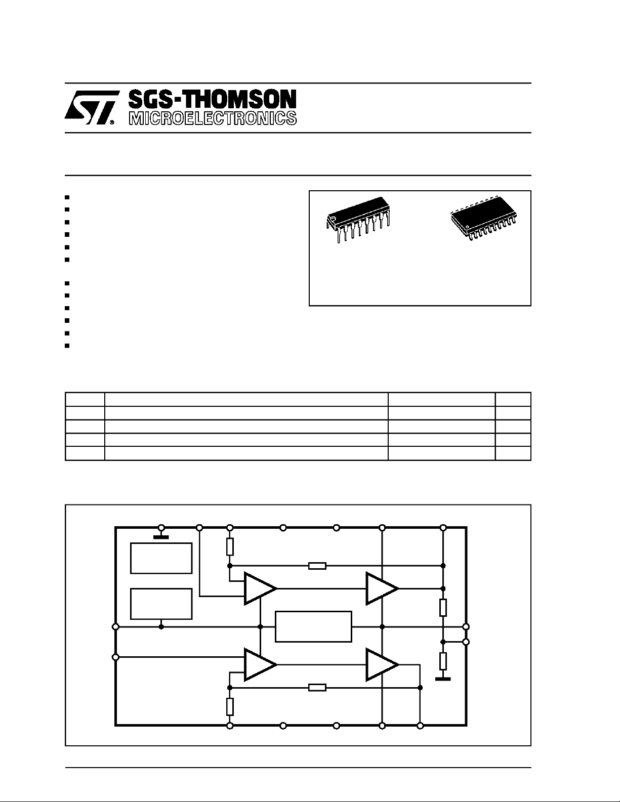
BLOCK DIAGRAM
OUT 1BOOT 1GNDGNDFEEDIN 1+GND(Sub)
THERMAL
PROTECT.
START
CIRCUIT
SVR
IN 2+
50Ω
10KΩ
-
+
DECOUPLING
2
+
10KΩ
11
5KΩ
V
S+
BRIDGE
2
50Ω
June 1994
D94AU120
50Ω
FEED GND GND BOOT 2 OUT 2
1/9
TEA2025B- TEA2025D
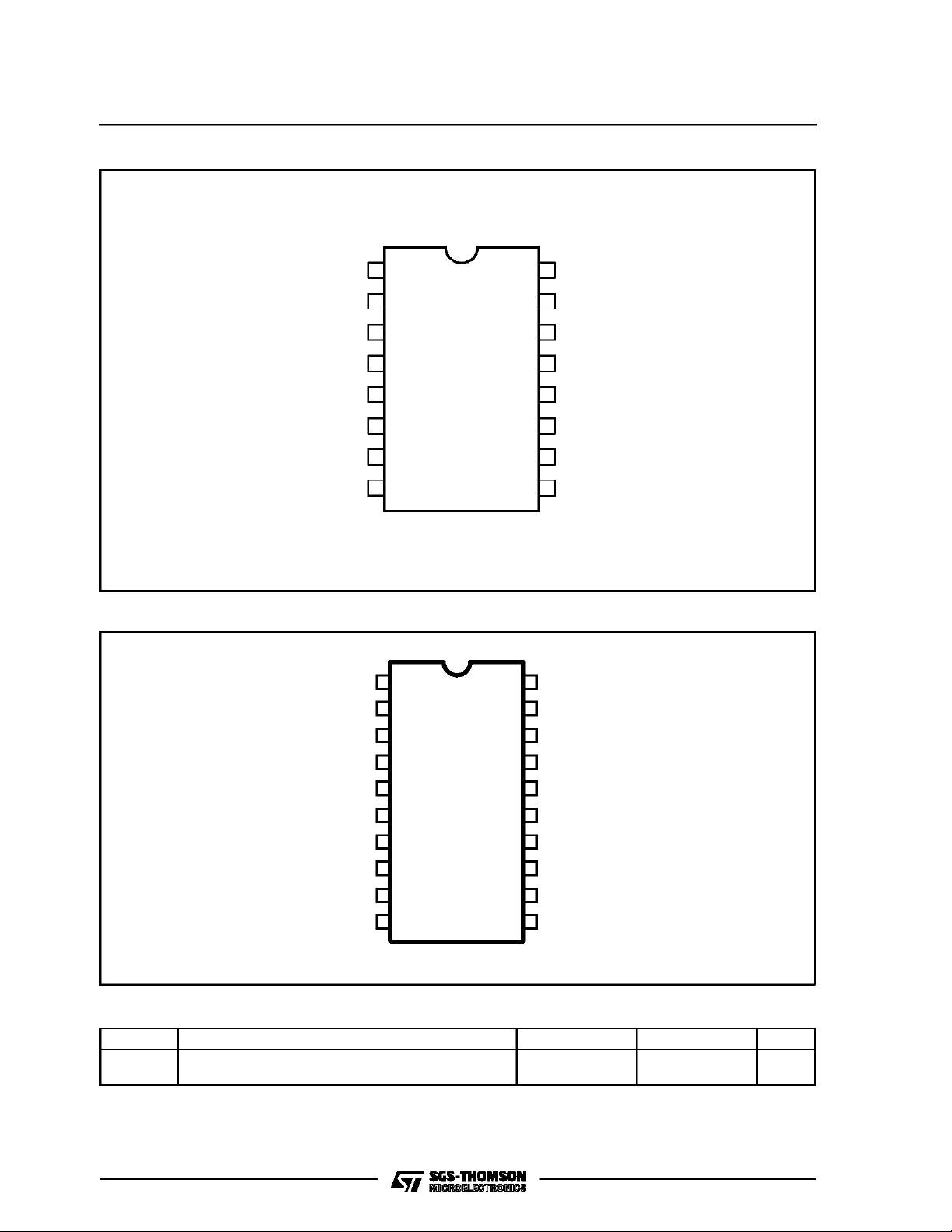
POWERDIP 12+2+2 PIN CONNECTION (Topview)
BRIDGE
OUT.2
BOOT.2
GND
GND
FEEDBACK
IN.2 (+)
SVR
SO12+4+4 PINCONNECTION (Top view)
BRIDGE
OUT 2
1
2
3
4
5
6
7
8
1
2
20
19
16
15
14
13
12
11
10
+Vs
OUT.1
BOOT.1
GND
GND
FEEDBACK
IN.1 (+)
9
GND (sub.)
V
CC
OUT 1
BOOT 2
GND
GND
GND
GND
FEEDBACK
IN 2(+)
3
4
5
6
7
8
9 IN 1(+)
18
17
16
15
14
13
12
BOOT 1
GND
GND
GND
GND
FEEDBACK
SVR 10 GND(Sub)11
D94AU119
THERMAL DATA
Symbol Description SO 12+4+4 (*) PDIP 12+2+2 (**) Unit
R
th j-case
R
th j-amb
(*) The R
(**) The R
2/9
Thermal ResistanceJunction-case
Thermal ResistanceJunction-ambient
is measured with 4sqcm copper area heatsink
th j-amb
is measured on devices bonded on a10 x 5 x 0.15cm glass-epoxy substrate with a35µm thick copper surface of 5 cm
th j-amb
Max
Max
15
65
15
60
°C/W
°C/W
2
.

TEA2025B - TEA2025D
ELECTRICAL CHARACTERISTICS (T
=25°C, VCC= 9V,Stereo unless otherwise specified)
amb
Symbol Parameter Test Conditions Min. Typ. Max. Unit
Supply Voltage 3 12 V
V
S
Quiescent Current 35 50 mA
I
Q
Quiescent OutputVoltage 4.5 V
V
O
A
Voltage Gain
V
∆A
Voltage Gain Difference ±1dB
V
Input Impedance 30 KΩ
R
j
PO
Output Power(d = 10%) Stereo 8 (per channel) 9V
Stereo
Bridge
Bridge
d Distortion Vs =9V; R
SVR Supply VoltageRejection f = 100Hz, V
=0
R
E
) Input Noise Voltage
N(IN
R
G
G
=104Ω
CT Cross-Talk f = 1KHz, R
4Ω
8Ω
9V
4Ω
6V
8Ω
6V
16Ω
6V
32Ω
6V
4Ω
3V
32Ω
3V
8Ω
12V
8Ω
9V
4Ω
6V
8Ω
6V
16Ω
3V
32Ω
3V
=4Ω
L
= 0.5V, Rg=0 40 46 dB
R
= 10KΩ
g
Stereo
Bridge
43
49
1.7
45
51
2.3
47
53
1.3
0.7
1
0.6
0.25
0.13
0.1
0.02
2.4
4.7
2.8
1.5
0.18
0.06
0.3
1.5
0.5
1.5
3
40 52 dB
3
6
dB
W
W
%
mV
Term. N° (PDIP) 1 2 3 4 5 6 7 8 9 10 11 12 13 14 15 16
DC VOLT (V) 0.04 4.5 8.9 0 0 0.6 0.04 8.5 0 0.04 0.6 0 0 8.9 4.5 9
Figure 1: Bridge Application(Powerdip)
Figure2: StereoApplication (Powerdip)
C1
C10
C2
C1 1
C3
C4
C8
C5
C9
C6
C7
3/9

TEA2025B- TEA2025D
Figure3: SupplyCurrent vs. SupplyVoltage
=4Ω)
(R
L
I(mA)
50
40
30
20
STEREO
10
3 6 9 12 15
Vs(V)
Figure5: OutputPower vs. Supply Voltage
(THD = 10%, f = 1KHz)
Po(W)
3.5
Figure4: OutputVoltage vs. SupplyVoltage
Vo(V)
8
7
6
5
4
3
2
1
0
3691215
Vs(V)Vs(V)
STEREO
Figure6: THDversus Output Power
THD(%)
10
(f = 1KHz, V
= 6V)
S
3
2.5
Rl=4ohm
2
1.5
1
0.5
0
3691215
Rl=8ohm
Vs(V)
Rl=16ohm
STEREO
Rl=16ohm
Rl=8ohm
Rl=4 OHM
1
0.1
STEREO
0 0.2 0.4 0.6 0.8 1
Po(W)
4/9

TEA2025B - TEA2025D
APPLICATIONINFORMATION
InputCapacitor
Inputcapacitor is PNP type allowingsource to be
referencedto ground.
In this way no input coupling capacitoris required.
However, a series capacitor(0.22 uF)to the input
sidecan be useful incase of noise due to variable
resistor contact.
Bootstrap
The bootstrap connection allows to increase the
output swing.
The suggested value for the bootstrapcapacitors
(100uF) avoids a reduction of the output signal
alsoat low frequenciesand low supply voltages.
Voltage Gain Adjust
STEREOMODE
The voltage gain is determined by on-chip resis-
tors R1 and R2 together with the external RfC1
seriesconnected betweenpin 6 (11)and ground.
The frequency response is given approximated
by:
V
OUT
V
IN
=
Rf + R2 +
R1
1
JWC1
With Rf=0, C1=100 uF, the gain results 46 dB
with pole at f=32Hz.
THE purpose of Rf is to reduce the gain. It is recommendedto notreduce it under 36 dB.
Thetotal gain of thebridge is givenby:
V
OUT
=
V
IN
andwith the suggestedvalues(C1 = C2 = 100 µF,
R1
Rf+R2 +
1
JWC1
(1+
R3
R4
R1
R2+R4+
1
JWC1
)
Rf=0) means:
Gv = 52 dB
Figure8
with first pole at f = 32 Hz
OutputCapacitors.
The low cut off frequency due to output capacitor
dependingon the load is given by:
2
ΠC
1
OUT•RL
F
=
L
BRIDGEMODE
Figure7
The bridge configuration is realized very easily
thanks to an internal voltage divider which provides(at pin 1) the CH 1 outputsignal after reduction. It is enough to connect pin 6 (invertinginput
of CH 2) witha capacitor to pin 1 and to connect
to ground the pin7.
with C
470µF and RL= 4 ohm it means FL=
OUT
80 Hz.
PopNoise
Most amplifiers similar to TEA 2025B need external resistors between DC outputs and ground in
order to optimize the pop on/off performance and
crossoverdistortion.
Figure9
The TEA 2025B solution allows to save components because of suchresistors(800 ohm)are includedinto the chip.
5/9

TEA2025B- TEA2025D
Stability
A good layout is recommended in order to avoid
oscillations.
Generally the designer must pay attention on the
followingpoints:
- Shortwires of componentsand short connections.
- No groundloops.
- Bypass of supplyvoltagewith capacitorsas
nearestas possible to the supply I.C.pin.The
low value(poliester)capacitorsmust have
good temperatureand frequencycharacteristics.
- No sockets.
2)the heatsink can have a smaller factorof safety
compared with that of a conventional circuit.
There is no device damage in the case of excessive junction temperature: all that happens
is that P
(and therefore P
O
) and Id are re-
tot
duced.
APPLICATIONSUGGESTION
The recommended values of the components are
those shown on stereo application circuit of
Fig. 2 different values can be used, the following table can help the designer.
COMPONENT
C1,C2 0.22µF INPUT DC
C3 100µF
C4,C5 100µF BOOTSTRAP
C6,C7 470µF
C8,C9 0.15µF
C10, C11 100µF
RECOMMENDED
VALUE
PURPOSE LARGER THAN SMALLER THAN
DECOUPLING IN
CASE OF SLIDER
CONTACT NOISE OF
VARIABLE
RESISTOR
RIPPLE REJECTON
OUTPUT DC
DECOUPLING
FREQUENCY
STABILITY
INVERTING INPUT
DC DECOUPLING
DEGRADATION OF
SVR, INCREASE OF
THD AT LOW
FREQUENCY AND
LOW VOLTAGE
INCREASE OF LOW
FREQUENCY CUTOFF
DANGER OF
OSCILLATIONS
INCREASE OF LOW
FREQUENCY CUTOFF
6/9

SO20PACKAGE MECHANICAL DATA
TEA2025B - TEA2025D
DIM.
MIN. TYP. MAX. MIN. TYP. MAX.
A 2.65 0.104
a1 0.1 0.3 0.004 0.012
a2 2.45 0.096
b 0.35 0.49 0.014 0.019
b1 0.23 0.32 0.009 0.013
C 0.5 0.020
c1 45 (typ.)
D 12.6 13.0 0.496 0.512
E 10 10.65 0.394 0.419
e 1.27 0.050
e3 11.43 0.450
F 7.4 7.6 0.291 0.299
L 0.5 1.27 0.020 0.050
M 0.75 0.030
S 8 (max.)
mm inch
7/9

TEA2025B- TEA2025D
DIP16 PACKAGE MECHANICAL DATA
DIM.
MIN. TYP. MAX. MIN. TYP. MAX.
a1 0.51 0.020
B 0.85 1.40 0.033 0.055
b 0.50 0.020
b1 0.38 0.50 0.015 0.020
D 20.0 0.787
E 8.80 0.346
e 2.54 0.100
e3 17.78 0.700
F 7.10 0.280
I 5.10 0.201
L 3.30 0.130
Z 1.27 0.050
mm inch
8/9

TEA2025B - TEA2025D
Information furnished is believedto be accurate and reliable. However,SGS-THOMSON Microelectronics assumes no responsibility for the
consequences of use of such informationnor for any infringement of patents or otherrights of third parties which may resultfrom itsuse. No
license is granted by implication or otherwise under any patent or patentrights of SGS-THOMSON Microelectronics. Specifications mentioned in this publication are subject to change without notice. This publication supersedesand replaces all informationpreviously supplied.
SGS-THOMSON Microelectronics products are not authorized for use as critical components in lifesupport devices or systems without express writtenapproval of SGS-THOMSON Microelectronics.
1994 SGS-THOMSON Microelectronics - All RightsReserved
SGS-THOMSON Microelectronics GROUP OF COMPANIES
Australia - Brazil- France - Germany -Hong Kong - Italy - Japan - Korea - Malaysia -Malta - Morocco - The Netherlands - Singapore-
Spain - Sweden - Switzerland - Taiwan - Thaliand- United Kingdom - U.S.A.
9/9

WWW.ALLDATASHEET.COM
Copyright © Each Manufacturing Company.
All Datasheets cannot be modified without permission.
This datasheet has been download from :
www.AllDataSheet.com
100% Free DataSheet Search Site.
Free Download.
No Register.
Fast Search System.
www.AllDataSheet.com
 Loading...