


Altivar 71
User's manual
Retain for future use
Modbus/Uni-Telway card
Modbus protocol
VW3 A3 303

Contents
1. Before you begin___________________________________________________________________________________________ 3
2. Documentation structure_____________________________________________________________________________________ 4
3. Introduction_______________________________________________________________________________________________ 5
3. 1. Presentation _____________________________________________________________________________________ ____ 5
3. 2. Notation ______________________________________________ ______________________________________________ 5
4. Hardware setup ___________________________________________________________________________________________ 6
4. 1. Receipt _________________________________________________________________________________________ ____ 6
4. 2. Hardware description __________________________________________________________________________________ 6
4. 3. Installing the card in the drive____________________________________________________________________________ 6
4. 4. Switch coding ________________________________________________________________________________________ 7
5. Connecting to the bus__________________________________________________________________ _____________________ 9
5. 1. Wiring recommendations _______________________________________________________________________________ 9
5. 2. Modbus RS485 standard __________________________________________________ _____________________________ 9
5. 3. Connection via RJ45 wiring system ______________________________________________________________________ 10
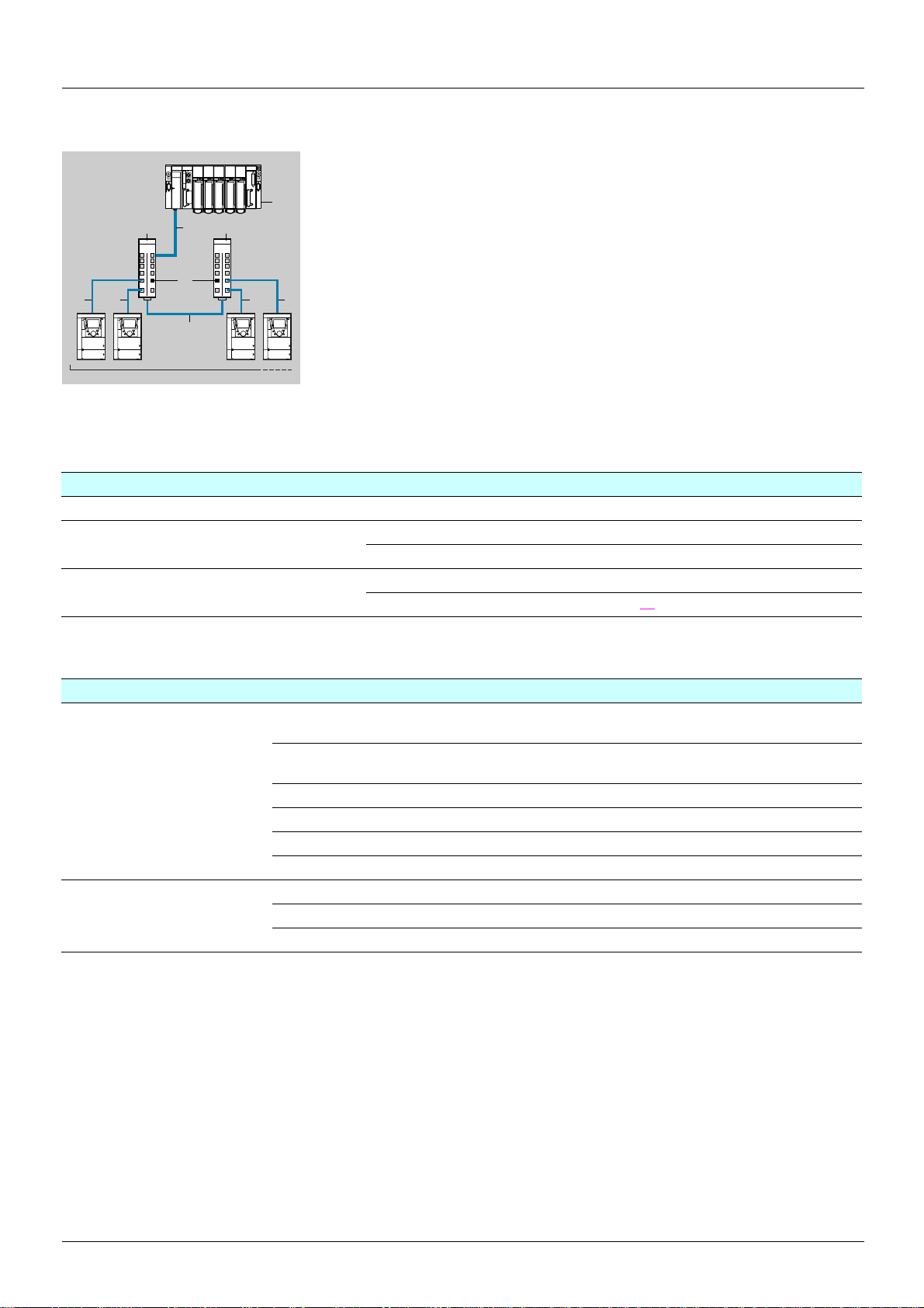
5. 4. Connection via junction boxes __________________________________________________________________________ 12
6. Configuration ____________________________________________________________________________________________ 14
6. 1. Communication parameters ____________________________________________________________________________ 14
6. 2. Control - Command __________________________________________________________________________________ 15
6. 3. Communication scanner_______________________________________________________________________________ 18
6. 4. Communication faults_________________________________________________________________________________ 19
6. 5. Monitored parameters________________________________ _________________________________________________ 20
7. Diagnostics______________________________________________________________________________________________ 21
7. 1. Checking the address_________________________________________________________________________________ 21
7. 2. LEDs______________________________________________________________________________________________ 21
7. 3. Control - Command __________________________________________________________________________________ 22
7. 4. Communication scanner_______________________________________________________________________________ 23
7. 5. Communication fault__________________________________________________________________________________ 24
7. 6. Card fault __________________________________________________________________________________________ 24
8. Modbus protocol__________________________________________________________________________________________ 25
8. 1. Principle __________________________________________________ _________________________________________ 25
8. 2. Modes_____________________________________________________________________________________________ 26
8. 3. Modbus functions available _______________________________ _____________________________________________ 27
8. 4. Read Holding/Input Registers (3/4) ______________________________________________________________________ 27
8. 5. Write Single Register (6)________________________________________________________________________ _______ 28
8. 6. Diagnostics (8) ______________________________________________________________________________________ 29
8. 7. Get Comm Event Counter (11 = 16#0B) __________________________________________________________________ 30
8. 8. Write Multiple Registers (16 = 16#10) ____________________________________________________________________ 30
8. 9. Read/Write Multiple Registers (23 = 16#17)____________________________________ ____________________________ 31
8. 10. Read Device Identification (43 = 16#2B) _________________________________________ ________________________ 32
8. 11. Communication scanner______________________________________________________________________________ 34
8. 12. Exception responses ________________________________________________________________________________ 37
8. 13. Read non-existent or protected parameters_______________________________________________________________ 38
9. Appendix________________________________________________________________________________________________ 39
9. 1. RS485 standard _____________________________________________________________________________________ 39
9. 2. Modbus 2-wire standard schematic ______________________________________________________________________ 40
9. 3. Modbus 4-wire standard schematic ______________________________________________________________________ 41
9. 4. Uni-Telway schematic_______________________ __________________________________________________________ 42
9. 5. 2-wire Jbus schematic ________________________________________________________________________________ 43
9. 6. Creating a Modbus bus using non-standard equipment_______________________________________________________ 44
9. 7. RS485 schematic for the card __________________________________________________________________________ 46
9. 8. Card connector pinout ________________________________________________________________________________ 46
While every precaution has been taken in the preparation of this document, Schneider
Electric SA assumes no liability for any omissions or errors it may contain, nor for any
damages resulting from the application or use of the information herein.
The products and options d escribed i n this document may be changed or modi fied at
any time, either from a technical point of view or in the way they are operated. Thei r
description can in no way be considered contractual.
2

1. Before you begin
Read and understand these instructions before performing any procedure with thi s drive.
DANGER
HAZARDOUS VOLTAGE
• Read and understand the Installation Ma nual before inst alling or op erating the Al tivar 71 drive. Installati on, adjustme nt,
repair, and maintenance must be performed by qualified personnel.
• The user is responsible for compliance with all international and national electrical standards in force concerning
protective grounding of all equipment.
• Many parts of this variable speed drive, including the printed circuit board s, operate at the line voltage. DO NOT TOUCH.
Use only electrically insulated tools.
• DO NOT touch unshielded components or terminal strip screw connections with voltage prese nt.
• DO NOT short across terminals PA/+ and PC/- or across the DC bus capacitors.
• Install and close all covers before applying power or starting and stopping the drive.
• Before servicing the variable speed drive
- Disconnect all power.
- Place a “DO NOT TURN ON” label on the variable speed drive disconnect.
- Lock the disconnect in the open position.
• Disconnect all power including external control power that may be present before servicing the drive. WAIT 15
MINUTES to allow the DC bus capacitors to discharge. Then follow the DC bus voltage measurement procedure given
in the installation manual to verify that the DC volta ge is less than 45 VDC. The drive LEDs are not accura te indi cators
of the absence of DC bus voltage.
Electric shock will result in death or serious injury.
CAUTION
EQUIPMENT DAMAGE
Do not operate or install any drive that appears damaged.
Failure to follow these instructions can result in equipment damage.
3

2. Documentation structure
The following Altivar 71 technical documents are availa ble on the Telemecanique website (www.telemecanique.com) as we ll as on the CDROM supplied with the drive.
b Installation Manual
This manual describes:
• How to assemble the drive
• How to connect the drive
b Programming Manual
This manual describes:
• The functions
• The parameters
• How to use the drive display terminal (integrated display terminal and graphic display terminal)
b Communication Parameters Manual
This manual describes:
• The drive parameters with specific information (addresses, formats, etc.) for use via a bus or communication network
• The operating modes specific to communication (state chart)
• The interaction between communication and local control
b Modbus, CANopen, Ethernet, Profibus, INTERBUS, Uni-Telway, DeviceNet, Modbus Plus and
FIPIO manuals
These manuals describe:
• Connection to the bus or network
• Configuration of the communication-specific parameters via the integrated display terminal or the graphic display terminal
• Diagnostics
• Software setup
• The communication services specific to the protocol
b Altivar 58/58F Migration Manual
This manual describes the differences between the Altivar 71 and the Altivar 58/58F.
It explains how to replace an Altivar 58 or 58F, including how to replace drives communicating on a bus or network.
4

3. Introduction
3. 1. Presentation
The communication card (catalog number VW3 A8 303) is used to connect an Altivar 71 drive to a Uni-Telway or Modbus bus.
This manual only describes how to use the Modbus protocol. For Uni-Telway, please refer to the Uni-Telway protocol manual.
The data exchanges permit access to all Altivar 71 functions:
• Configuration
• Adjustment
• Control and command
• Monitoring
• Diagnostics
The card has a female 9-way SUB-D connector for connection to the Modbus bus.
The connection cables and accessories should be ordered separately.
The drive address should be configured using the switches on the card.
The graphic display terminal or the integrated display terminal offer numerous functions for communication diagnosti cs.
Note: The Modbus card supports the following services in addition to those provided by the drive’s integrated ports:
- 2-wire and 4-wire RS485
- Choice of line polarization
- RTU and ASCII modes
- More diagnostic subcodes
- More Modbus functions (04: Read Input Registers and 11: Get Comm Event Counter)
3. 2. Notation
Drive terminal displays
The graphic display terminal menus are shown in square brackets.
Example: [1.9 COMMUNICATION]
The integrated 7-segment display terminal menus are shown in round brackets.
Example: (COM-)
Parameter names displayed on the graphic display terminal are shown in square brackets.
Example: [Fallback speed]
Parameter codes displayed on the integrated 7-segment display terminal are shown in round brackets.
Example: (LFF)
Formats
Hexadecimal values are written as follows: 16#
Binary values are written as follows: 2#
Abbreviations
Hi: High order
Lo: Low order
5

4. Hardware setup
4. 1. Receipt
Check that the card catalog number marked on the label is the same as that on the delivery note corresponding to the purchase order.
Remove the option card from its packaging and check that it has not been damaged in transit.
4. 2. Hardware description
LEDs
Female 9-way SUB-D connector
Polarization switches
4. 3. Installing the card in the drive
See the Installation Manual.
Address switches
6

4. Hardware setup
4. 4. Switch coding
b Choosing polarization
Normal setting for a Modbus bus:
• No polarization at drive level
Special setting (see "Creating a Modbus bus using non-standard equipment" on page 44
Ω RS485 line polarization at drive level
• 4.7 k
b Coding the address
The address switches are used to encode the address (1 to 247) of the drive on the bus.
The switch settings can only be changed when the drive is turned off.
The correspondence between the value and the position of the switch is as follows:
• 0 = OFF = Switch in upper position
• 1 = ON = Switch in lower position
The address is binary-coded.
Examples:
Address 11 = 2#0000 1011
Address 34 = 2#0010 0010
):
7

4. Hardware setup
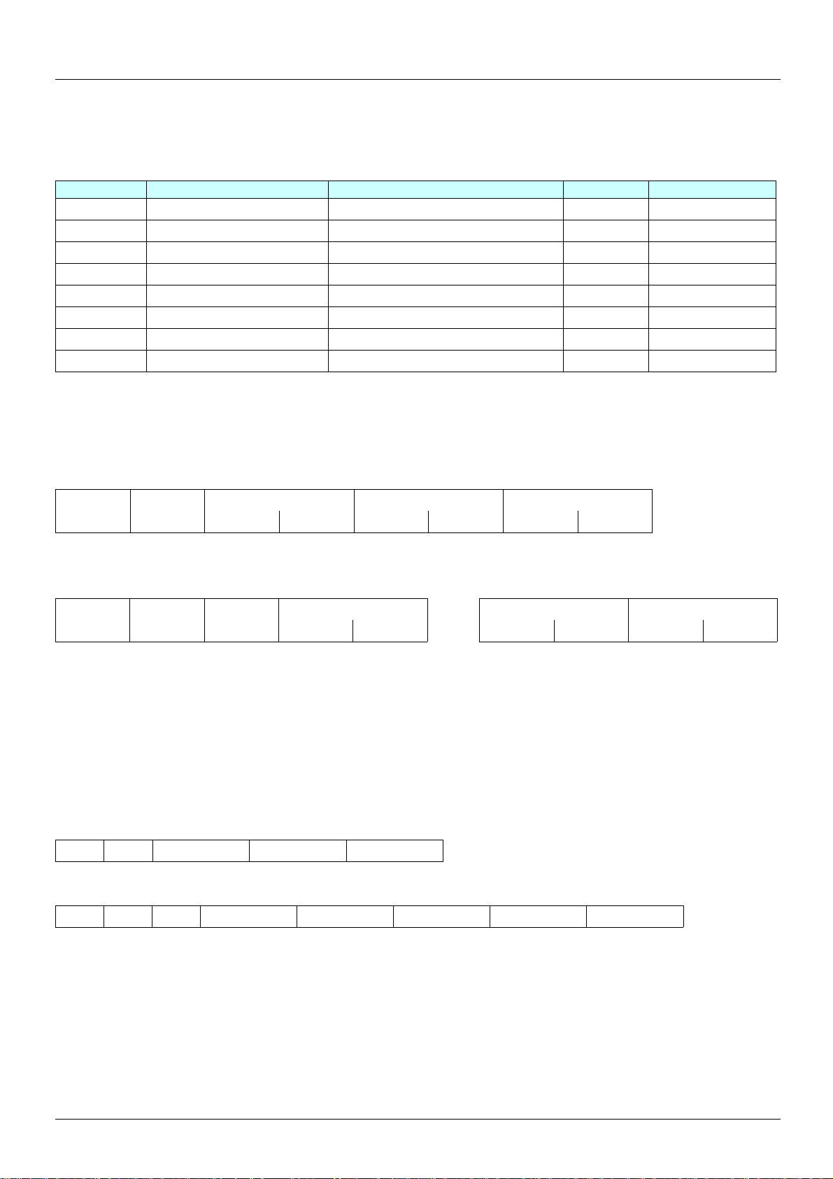
The table below indicates the positions of the 8 switches for all configurable addresses:
Address Switches
1234 5678
0 0000 0000 052 0011 0100 104 0110 1000 156 1001 1100 208 1101 0000
001 0000 0001 053 0011 0101 105 0110 1001 157 1001 1101 209 1101 0001
002 0000 0010 054 0011 0110 106 0110 1010 158 1001 1110 210 1101 0010
003 0000 0011 055 0011 0111 107 0110 1011 159 1001 1111 211 1101 0011
004 0000 0100 056 0011 1000 108 0110 1100 160 1010 0000 212 1101 0100
005 0000 0101 057 0011 1001 109 0110 1101 161 1010 0001 213 1101 0101
006 0000 0110 058 0011 1010 110 0110 1110 162 1010 0010 214 1101 0110
007 0000 0111 059 0011 1011 111 0110 1111 163 1010 0011 215 1101 0111
008 0000 1000 060 0011 1100 112 0111 0000 164 1010 0100 216 1101 1000
009 0000 1001 061 0011 1101 113 0111 0001 165 1010 0101 217 1101 1001
010 0000 1010 062 0011 1110 114 0111 0010 166 1010 0110 218 1101 1010
011 0000 1011 063 0011 1111 115 0111 0011 167 1010 0111 219 1101 1011
012 0000 1100 064 0100 0000 116 0111 0100 168 1010 1000 220 1101 1100
013 0000 1101 065 0100 0001 117 0111 0101 169 1010 1001 221 1101 1101
014 0000 1110 066 0100 0010 118 0111 0110 170 1010 1010 222 1101 1110
015 0000 1111 067 0100 0011 119 0111 0111 171 1010 1011 223 1101 1111
016 0001 0000 068 0100 0100 120 0111 1000 172 1010 1100 224 1110 0000
017 0001 0001 069 0100 0101 121 0111 1001 173 1010 1101 225 1110 0001
018 0001 0010 070 0100 0110 122 0111 1010 174 1010 1110 226 1110 0010
019 0001 0011 071 0100 0111 123 0111 1011 175 1010 1111 227 1110 0011
020 0001 0100 072 0100 1000 124 0111 1100 176 1011 0000 228 1110 0100
021 0001 0101 073 0100 1001 125 0111 1101 177 1011 0001 229 1110 0101
022 0001 0110 074 0100 1010 126 0111 1110 178 1011 0010 230 1110 0110
023 0001 0111 075 0100 1011 127 0111 1111 179 1011 0011 231 1110 0111
024 0001 1000 076 0100 1100 128 1000 0000 180 1011 0100 232 1110 1000
025 0001 1001
026 0001 1010 078 0100 1110 130 1000 0010 182 1011 0110 234 1110 1010
027 0001 1011 079 0100 1111 131 1000 0011 183 1011 0111 235 1110 1011
028 0001 1100 080 0101 0000 132 1000 0100 184 1011 1000 236 1110 1100
029 0001 1101 081 0101 0001 133 1000 0101 185 1011 1001 237 1110 1101
030 0001 1110 082 0101 0010 134 1000 0110 186 1011 1010 238 1110 1110
031 0001 1111 083 0101 0011 135 1000 0111 187 1011 1011 239 1110 1111
032 0010 0000 084 0101 0100 136 1000 1000 188 1011 1100 240 1111 0000
033 0010 0001 085 0101 0101 137 1000 1001 189 1011 1101 241 1111 0001
034 0010 0010 086 0101 0110 138 1000 1010 190 1011 1110 242 1111 0010
035 0010 0011 087 0101 0111 139 1000 1011 191 1011 1111 243 1111 0011
036 0010 0100 088 0101 1000 140 1000 1100 192 1100 0000 244 1111 0100
037 0010 0101 089 0101 1001 141 1000 1101 193 1100 0001 245 1111 0101
038 0010 0110 090 0101 1010 142 1000 1110 194 1100 0010 246 1111 0110
039 0010 0111 091 0101 1011 143 1000 1111 195 1100 0011
040 0010 1000 092 0101 1100 144 1001 0000 196 1100 0100 1111 1000
041 0010 1001 093 0101 1101 145 1001 0001 197 1100 0101 1111 1001
042 0010 1010 094 0101 1110 146 1001 0010 198 1100 0110 1111 1010
043 0010 1011 095 0101 1111 147 1001 0011 199 1100 0111 1111 1011
044 0010 1100 096 0110 0000 148 1001 0100 200 1100 1000 1111 1100
045 0010 1101 097 0110 0001 149 1001 0101 201 1100 1001 1111 1101
046 0010 1110 098 0110 0010 150 1001 0110 202 1100 1010 1111 1110
047 0010 1111 099 0110 0011 151 1001 0111 203 1100 1011 1111 1111
048 0011 0000 100 0110 0100 152 1001 1000 204 1100 1100
049 0011 0001 101 0110 0101 153 1001 1001 205 1100 1101
050 0011 0010 102 0110 0110 154 1001 1010 206 1100 1110
051 0011 0011 103 0110 0111 155 1001 1011 207 1100 1111
Address Switches
1234 5678
077 0100 1101 129 1000 0001 181 1011 0101 233 1110 1001
Address Switches
1234 5678
Address Switches
1234 5678
Address Switches
1234 5678
1111 0111
247
Note: Address 0 is not valid.
8

5. Connecting to the bus
5. 1. Wiring recommendations
• Use Telemecanique-approved cables and wiring accessories to ensure good transmission quality (matched impedance, immunity,
shielding connection, etc.).
• Keep the Modbus cable away from the power cables (30 cm minimum).
• Be sure to cross the Modbus cable and the power cables at right angles.
• Whenever possible, connect the bus cable shiel ding to the protective ground, e.g., to th e ground of each device if this ground is connected
to the protective ground.
• Install a line terminator at both ends of the line.
• Ensure the correct line polarization.
• Connect the common polarity ("Common" signal) to the protective ground at one or more points on the bus.
For more information, please refer to the TSX DG KBL E guide: "Electromagnetic compatibility of industrial networks and fieldbuses".
5. 2. Modbus RS485 standard
The characteristics and accessories mentioned in this section ("5. Connecting to the bus") comply with the Modbus standard.
Other non-Modbus-standard RS485 wiring diagrams are possible. Please see the Appendix for further information.
The latest generation of Telemecanique equipment conforms to Modbus (2-wire RS485).
Main characteristics:
Maximum length of bus 1000 m at 19,200 bps
Maximum number of stations 32 stations, i.e., 31 slaves (without repeater)
9
5. Connecting to the bus
5. 3. Connection via RJ45 wiring system
1. Master (PLC, PC or communication module)
2. Cable depending on the type of master (see table)
3. Splitter block LU9 GC3
4. Drop cable VW3 A58 306 Rpp
5. Line terminators VW3A8306RC
44
6. Modbus cable TSX CSA p00
A TV 71
1
3
44
3
2
5
6
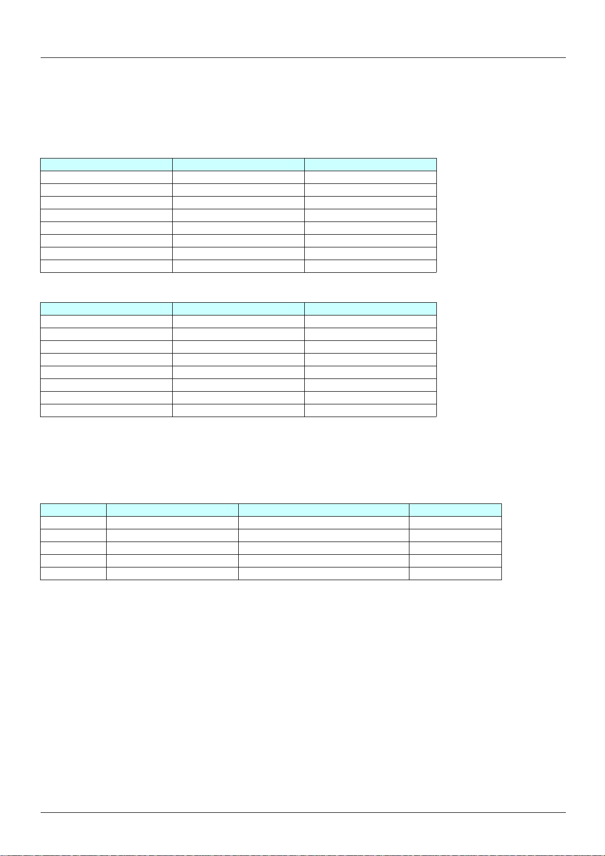
b Connection accessories
Description Ref. Catalog number
Modbus splitter block 10 RJ45 connectors and 1 screw terminal block 3 LU9 GC3
Modbus T-junction boxes With integrated cable (0.3 m) VW3 A8 306 TF03
With integrated cable (1 m) VW3 A8 306 TF10
Line terminators
For RJ45 connector
R = 120 Ω, C = 1 nF 5 VW3 A8 306 RC
R = 150 Ω (specific to "Jbus schematic" page 43
)5 VW3A8306R
b Connection cables
Description Length (m) Connectors Ref. Catalog number
Cables for Modbus bus 1 1 RJ45 connector and
1 male 9-way SUB-D connector
3 1 RJ45 connector and
1 male 9-way SUB-D connector
3 1 RJ45 connector and 1 stripped end VW3 A8 306 D30
0.3 2 RJ45 connectors VW3 A8 306 R03
1 2 RJ45 connectors VW3 A8 306 R10
3 2 RJ45 connectors VW3 A8 306 R30
RS485 double shielded twisted
pair cables
100 Supplied without connector 6 TSXCSA 100
200 Supplied without connector 6 TSXCSA 200
500 Supplied without connector 6 TSXCSA 500
4 VW3 A58 306 R10
4 VW3 A58 306 R30
10

5. Connecting to the bus
b Connection cables for the master
Type of master Master interface Description Catalog number
Twido PLC Adaptor or mini-DIN
RS485 interface module
Adaptor or screw
terminal RS485
interface module
TSX Micro PLC Mini-DIN RS485
connector port
PCMCIA card
(TSX SCP114)
TSX Premium PLC TSX SCY 11601 or
TSX SCY 21601
module
(25-way SUB-D socket)
PCMCIA card
(TSX SCP114)
Ethernet bridge
(174 CEV 300 20)
Profibus DP gateway
(LA9P307)
Fipio (LUFP1) or
Profibus DP (LUFP7) or
DeviceNet (LUFP9)
gateway
Serial port PC Male 9-way SUB-D
Screw terminal RS485 3 m cable equipped with an RJ45 connector and stripped at
RJ45 RS485 1 m cable equipped with 2 RJ45 connectors VW3 P07 306 R10
RJ45 RS485 0.3 m cable equipped with 2 RJ45 connectors or
RS232 serial port PC
3 m cable equipped with a mini-DIN connect or and an RJ45
connector
3 m cable equipped with an RJ45 connector and stripped at
the other end
3 m cable equipped with a mini-DIN connect or and an RJ45
connector
Stripped cable TSX SCP CM 4030
Cable equipped with a 25-way SUB-D connector and
stripped at the other end (for connection to the screw
terminals of the LU9GC3 splitter block)
Stripped cable TSX SCP CM 4030
the other end
1 m cable equipped with 2 RJ45 connectors or
3 m cable equipped with 2 RJ45 connectors
RS232/RS485 converter and 3 m cable equipped with an
RJ45 connector and stripped at the other end (for
connection to the screw terminals of the LU9GC3 splitter
block)
TWD XCA RJ030
VW3 A8 306 D30
TWD XCA RJ030
TSX SCY CM 6030
VW3 A8 306 D30
VW3 A8 306 R03 or
VW3 A8 306 R10 or
VW3 A8 306 R30
TSX SCA 72 and
VW3 A8 306 D30
11

5. Connecting to the bus
5. 4. Connection via junction boxes
1. Master (PLC, PC or communication module)
2. Modbus cable depending on the type of master (see table)
1
32
44
3. Modbus cable TSX CSAp00
4. Subscriber sockets TSX SCA 62
5. Modbus drop cable VW3A83062
A TV 71
6
6
b Connection accessories
Description Ref. Catalog
number
Subscriber socket
2 female 15-way SUB-D connectors, 2 screw terminals, and an RC line terminator,
to be connected using cable VW3 A8 306 or VW3 A8 306 D30
4 TSX SCA 62
b Connection cables
Description Length (m) Connectors Ref. Catalog
number
Cables for Modbus bus 3 1 9-way SUB-D connector and
1 male 15-way SUB-D connector
for TSX SCA 62
RS485 double shielded twisted pair
cables
100 Supplied without connector 3 TSX CSA 100
200 Supplied without connector 3 TSX CSA 200
500 Supplied without connector 3 TSX CSA 500
6 VW3 A8 306 2
12

5. Connecting to the bus
b Connection cables for the master
Type of master Master interface Description Catal og number
Twido PLC Adaptor or screw terminal
RS485 interface module
TSX Micro PLC Mini-DIN RS485
connector port
PCMCIA card (TSX SCP114) Cable equipped with a special connector and
TSX Premium PLC TSX SCY 11601 or
TSX SCY 21601 module
(25-way SUB-D socket)
PCMCIA card (TSX SCP114) Cable equipped with a special connector and
Ethernet bridge
(174 CEV 300 10)
Profibus DP gateway
(LA9P307)
Fipio (LUFP1) or
Profibus DP (LUFP7) or
DeviceNet (LUFP9) gateway
Serial port PC Male 9-way SUB-D RS232
Screw terminal RS485 Modbus cable TSX CSA100 or
RJ45 RS485 3 m cable equipped with an RJ45 connector
RJ45 RS485 3 m cable equipped with an RJ45 connector
serial port PC
Modbus cable TSX CSA100 or
TSX CSA200 or
TSX CSA500
Tap junction TSX P ACC 01
TSX SCP CM 4030
stripped at the other end
Cable equipped with a 25-way SUB-D
connector and stripped at the other end
stripped at the other end
and stripped at the other end
and stripped at the other end
RS232/RS485 converter and
Modbus cable
TSX SCY CM 6030
TSX SCP CM 4030
TSX CSA200 or
TSX CSA500
VW3 A8 306 D30
VW3 A8 306 D30
TSX SCA 72 and
TSX CSA100 or
TSX CSA200 or
TSX CSA500
13

6. Configuration
6. 1. Communication parameters
Configure the following parameters in the [1.9 - COMMUNICATION] (COM-) menu, [Uni-Telway/Modbus] (UtL-) submenu:
[Protocol] (PrO), [Bit rate] (bdr) and [Format] (FOr).
These parameters can only be modified when the motor is stopped. Modifications can only be taken into account by the drive following a
power break.
Parameter Possible values Terminal display Default value
[Protocol]
(PrO)
[Address]
(AdrC)
[Bit rate]
(Bdr)
[Format]
(FOr)
Uni-Telway
Modbus/RTU
Modbus/ASCII
0 to 247 [0] (0) to [247] (247) Value taken from the address switches
4800 bps
9600 bps
19,200 bps
In RTU mode only:
8 data bits, odd parity, 1 stop bit
8 data bits, even parity, 1 stop bit
8 data bits, no parity, 1 stop bit
8 data bits, no parity, 2 stop bits
In RTU and ASCII modes:
7 data bits, odd parity, 1 stop bit
7 data bits, even parity, 1 stop bit
7 data bits, odd parity, 2 stop bits
7 data bits, even parity, 2 stop bits
[Unitelway] (UtE)
[Modbus RTU] (rtU)
[Modbus ASCII] (ASC)
[4800 Bd] (
[9600 Bd] (
[19200 Bd] (
[8-O-1] (8o1)
[8-E-1] (8E1)
[8-N-1] (8n1)
[8-N-2] (8n2)
[7-O-1] (7o1)
[7-E-1] (7E1)
[7-O-2] (7o2)
[7-E-2] (7E2)
48)
96)
19 2)
[Unitelway] (UtE)
[19.2 Kbps] (
[8-O-1] (8o1)
19 2)
14

6. Configuration
6. 2. Control - Command
Numerous configurations are possible. For more information, refer to the Programming Manual and th e Parameters Manual.
The following configurations are just some of the possibili ties available.
b Control via Modbus in I/O profile
The command and reference come from Modbus.
The command is in I/O profile.
Configure the following parameters:
Parameter Value Comment
Profile I/O profile The run command is simply obtained by bit 0 of the control word.
Reference 1 configuration Network card The reference comes from Modbus.
Command 1 configuration Network card The command comes from Modbus.
Configuration via the graphic display terminal or the integrated display terminal:
Menu Parameter Value
[1.6 - COMMAND] (CtL-) [Profile]
(CHCF) [I/O profile] (IO)
[Ref.1 channel] (Fr1) [Com. card] (nEt)
[Cmd channel 1] (Cd1) [Com. card]
(nEt)
b Control via Modbus or the terminals in I/O profile
Both the command and reference come from Modbus or the terminals. Input LI5 at the terminals is used to switch between Modbus and the
terminals.
The command is in I/O profile.
Configure the following parameters:
Parameter Value Comment
Profile I/O profile The run command is simply obtained by bit 0 of the control word.
Reference 1 configuration Network card Reference 1 comes from Modbus.
Reference 1B configuration Analog input 1 on the termi nals Reference 1B comes from input AI1 on the terminals.
Reference switching Input LI5 Input LI5 switches the reference (1
Command 1 configuration Network card Command 1 comes from Modbus.
Command 2 configuration Terminals Command 2 comes from the terminals.
Command switching Input LI5 Input LI5 switches the command.
Note: Reference 1B is directly connected to the drive reference limit. If switching is performed, the functions that affect the reference
(summing, PID, etc) are inhibited.
Configuration via the graphic display terminal or the integrated display terminal:
Menu Parameter Value
[1.6 - COMMAND] (CtL-) [Profile] (CHCF) [I/O profile] (IO)
[1.7 APPLICATION FUNCT.] (FUn-)
[REFERENCE SWITCH.]
[Ref.1 channel]
[Cmd channel 1]
[Cmd channel 2] (Cd2) [Terminals] (tEr)
[Cmd switching] (CCS) [LI5] (LI5)
[Ref.1B channel] (Fr1b) [Ref. AI1] (AI1)
[Ref 1B switching] (rCb) [LI5] (LI5)
(Fr1) [Com. card] (nEt)
(Cd1) [Com. card] (nEt)
↔1B).
15
6. Configuration
b Control via Modbus in Drivecom profile
The command and reference come from Modbus.
The command is in Drivecom profile.
Configure the following parameters:
Parameter Value Comment
Profile Drivecom profile not
separate
Reference 1 configuration Network card The command comes from Modbus.
Configuration via the graphic display terminal or the integrated display terminal:
Menu Parameter Value
[1.6 - COMMAND] (CtL-) [Profile] (CHCF) [Not separ.] (SIM) (factory setting)
[Ref. 1] (Fr1) [Com. card] (nEt)
b Control via Modbus or the terminals in Drivecom profile
Both the command and reference come from Modbus or the terminals. Input LI5 at the terminals is used to switch between Modbus and the
terminals.
The command is in Drivecom profile.
The run commands are in Drivecom profile, the command and the reference
come from the same channel.
Configure the following parameters:
Parameter Value Comment
Profile Drivecom profile not separate The run commands follow the Drivecom profile, and the command and
Reference 1 configuration Network card Reference 1 comes from Modbus.
Reference 2 configuration Analog input 1 on the terminals Reference 2 comes from input AI1 on the terminals.
Reference switching Input LI5 Input LI5 switches the reference (1
Caution: Reference 2 is directly connected to the drive reference limit. If switching is performed, the functions that affect the reference
(summing, PID, etc) are inhibited.
Configuration via the graphic display terminal or the integrated display terminal:
Menu Parameter Value
[1.6 - COMMAND] (CtL-) [Profile] (CHCF) [Not separ.] (SIM)
[Ref.1 channel] (Fr1) [Com. card] (nEt)
[Ref.2 channel] (Fr2) [Ref. AI1] (AI1)
[Ref. 2 switching] (rFC) [LI5] (LI5)
reference come from the same channel.
↔ 2) and the command.
16
6. Configuration
b Control in Drivecom profile via Modbus and reference switching at the terminals
The command comes from Modbus.
The command comes either from Modbus or from the terminals. Input LI5 at the t erminals is used to switch the referenc e between Modbus
and the terminals.
The command is in Drivecom profile.
Configure the following parameters:
Parameter Value Comment
Profile Separate Drivecom profile The run commands follow the Drivecom profile, and the command and
Reference 1 configuration Network card Reference 1 comes from Modbus.
Reference 1B configuration Analog input 1 on the terminals Reference 1B comes from input AI1 on the terminals.
Reference switching Input LI5 Input LI5 switches the reference (1
Command 1 configuration Network card Command 1 comes from Modbus.
Command switching Channel 1 Channel 1 is the command channel.
Note: Reference 1B is directly connected to the drive reference limit. If switching is performed, the functions that affect the reference
(summing, PID, etc) are inhibited.
Configuration via the graphic display terminal or the integrated display terminal:
reference can come from different channels.
↔1B).
Menu Parameter Value
[1.6 - COMMAND] (CtL-) [Profile] (CHCF) [Separate] (SEP)
[Ref.1 channel] (Fr1) [Com. card] (nEt)
[Cmd channel 1] (Cd1) [Com. card] (nEt)
[Cmd switching] (CCS) [ch1 active] (Cd1)
[1.7 APPLICATION FUNCT.] (FUn-)
[REFERENCE SWITCH.]
[Ref.1B channel] (Fr1b) [Ref. AI1] (AI1)
[Ref 1B switching] (rCb) [LI5] (LI5)
17
6. Configuration
6. 3. Communication scanner
The communication scanner enables all the applicatio n-relevant parameters to be grouped in 2 co nsecutive word tables so that singl e read
and write operations may be performed. It is even possible to perform a si ngle transact ion usi ng the "Rea d/Write Multi ple Re gist ers" (23 =
16#17) function.
The 8 output variables are assigned using the 8 [Scan.Outp address] (nCAp) parameters. They are configured using the graphic display
terminal via the [1.9 - COMMUNICATION] (COM-) menu, [COM. SCANNER OUTPUT] (OCS-) submenu.
The 8 input variables are assigned using the 8 [Scan. INp address] (nMAp) parameters. They are configured using the graphic display
terminal via the [1.9 - COMMUNICATION] (COM-) menu, [COM. SCANNER INPUT] (ICS-) submenu.
Enter the logic address of the parameter (see the Parameters Manual).
If a [Scan.Outp address] (nCAp) or [Scan. INp address] (nMAp) parameter equals zero, the corresponding variable is not used by the
drive.
These 16 assignment parameters are described in the tables below:
Configuration parameter name Default assignment of the output variable
[Scan. Out1 address] (nCA1) Control word (CMd)
[Scan. Out2 address] (nCA2) Speed reference (LFrd)
[Scan. Out3 address] (nCA3) Not used
[Scan. Out4 address] (nCA4) Not used
[Scan. Out5 address] (nCA5) Not used
[Scan. Out6 address] (nCA6) Not used
[Scan. Out7 address] (nCA7) Not used
[Scan. Out8 address] (nCA8) Not used
Configuration parameter name Default assignment of the input variable
[Scan. IN1 address] (nMA1) Status word (EtA)
[Scan. IN2 address] (nMA2) Output speed (rFrd)
[Scan. IN3 address] (nMA3) Not used
[Scan. IN4 address] (nMA4) Not used
[Scan. IN5 address] (nMA5) Not used
[Scan. IN6 address] (nMA6) Not used
[Scan. IN7 address] (nMA7) Not used
[Scan. IN8 address] (nMA8) Not used
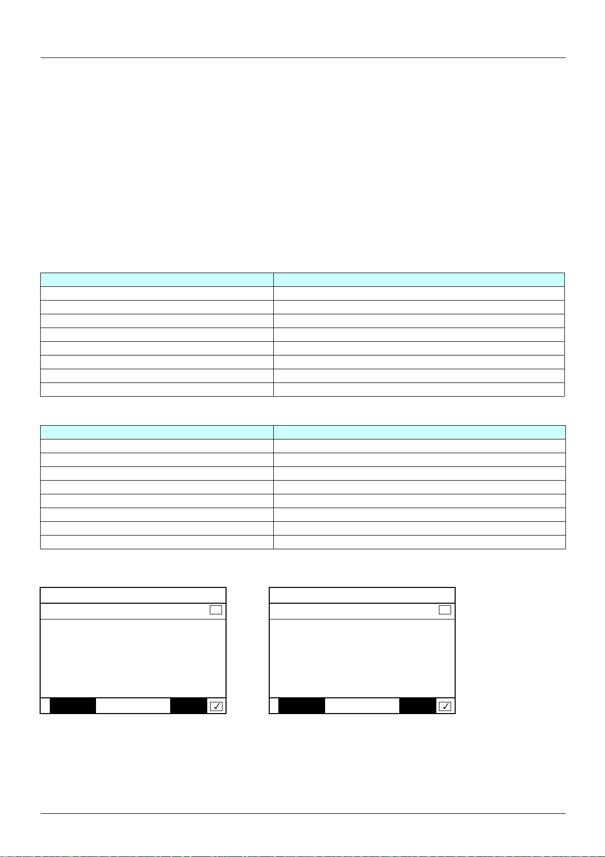
Example of configuration via the graphic display terminal:
RDY NET +0.00Hz 0A RDY NET +0.00Hz 0A
COM. SCANNER INPUT COM. SCANNER OUTPUT
Scan. IN1 address : 3201 Scan. Out1 address : 8501
Scan. IN2 address : 8604 Scan. Out2 address : 8602
Scan. IN3 address : 0 Scan. Out3 address : 0
Scan. IN4 address : 0 Scan. Out4 address : 0
Scan. IN5 address : 0 Scan. Out5 address : 0
Code Quick Code Quick
Scan. IN6 address : 0 Scan. Out6 address : 0
Scan. IN7 address : 0 Scan. Out7 address : 0
Scan. IN8 address : 0 Scan. Out8 address : 0
Note:
Any modification to parameters [Scan.Outp address] (nCAp) or [Scan. INp address] (nMAp) must be made with the motor stopped. The
master PLC program should be updated to take account of this modification.
18

6. Configuration
6. 4. Communication faults
A Modbus fault is triggered if the Modbus card does not receive any Modbus requests at its address within a predefined time period (time
out). All Modbus request types are taken into account (read, write, etc.). The time out is fixed at 10 s (non-modifiable).
The response of the drive in the event of a Modbus communication fault can be configured.
RDY NET +0.00Hz 0A
COM. FAULT MANAGEMENT
Configuration can be performed using the graphic display terminal or
integrated display terminal using the [Network fault mgt] (CLL)
parameter in the [1.8 FAULT MANAGEMENT] (FLt-) menu, [COM.
FAULT MANAGEMENT] (CLL-) submenu.
The values of the [Network fault mgt] (CLL) parameter, which trigger a [Com. network] (CnF) drive fault, are:
Value Meaning
[Freewheel] (YES) Freewheel stop (factory setting)
[Ramp stop] (rMP) Stop on ramp
[Fast stop] (FSt) Fast stop
[DC injection]
(dCI) DC injection stop
Network fault mgt : Freewheel
CANopen fault mgt : Freewheel
Modbus fault mgt : Freewheel
Code Quick
The values of the [Network fault mgt] (CLL) parameter, which do not trigger a drive fault, are:
Value Meaning
[Ignore] (nO) Fault ignored
[Per STT] (Stt) Stop according to configuration of [Type of stop]
[fallback spd] (LFF) Switch to f allback speed, maintain ed as long as the faul t is present and the run command is not disabled.
[Spd maint.]
The fallback speed can be configured via the [Fallback speed]
(rLS)
The drive maintains the speed at the time the fault occurred, as long as the fault persists and the run
command has not been removed.
(LFF) parameter in the [1.8 – FAULT MANAGEMENT] (FLt-) menu.
(Stt).
19
6. Configuration
6. 5. Monitored parameters
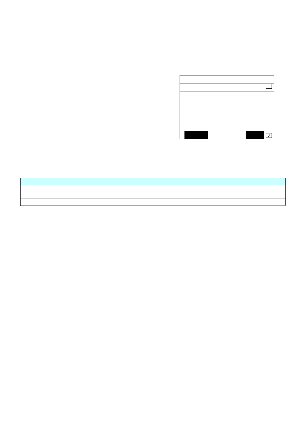
It is possible to select up to 4 parameters to display their values in the [1.2 - MONITORING] menu ([COMMUNICATION MAP] submenu)
on the graphic display terminal.
The selection is made via the [6 – MONITOR CONFIG.] menu ([6.3 - CONFIG. COMM. MAP] submenu).
Each parameter [Address 1 select] ... [Address 4 selec t] can be used to
choose the logic address of the parameter. Select an address of zero
to disable the function.
In the example given here, the monitored words are:
• Parameter 1 = Motor current (LCr): logic address 3204;
signed decimal format
• Parameter 2 = Motor torque (Otr): logic address 3205; signed
decimal format
• Parameter 3 = Last fault occurred (LFt): logic address 7121;
hexadecimal format
• Disabled parameter: address 0; default format: hexadecimal format
RDY NET +0.00Hz 0A
6.3 CONFIG. COMM. MAP.
Address 1 select : 3204
FORMAT 1 : Signed
Address 2 select : 3205
FORMAT 2 : Signed
Address 3 select : 7121
Code Quick
FORMAT 3 : Hex
Address 4 select : 0
FORMAT 4 : Hex
One of the three display formats below can be assigned to each monitored word:
Format Range Terminal display
Hexadecimal 0000 ... FFFF [Hex]
Signed decimal -32,767 ... 32,767 [Signed]
Unsigned decimal 0 ... 65,535 [Unsigned]
20

7. Diagnostics
2.1
2.2
7. 1. Checking the address
On the graphic display terminal or integrated dis play te rmi na l, chec k th e add ress t hat has been code d on the switches usi ng t he [Address]
(AdrC) parameter in the [1.9 COMMUNICATION] (COM-) menu, [Uni-Telway / Modbus] (UtL-) submenu.
This parameter cannot be modified.
7. 2. LEDs
The Modbus card has 2 LEDs, RUN and ERR, which are visible through the drive cover.
1.1
1.2
1.3
1.4
1.5
RUN (green)
2.3
2.4
2.5
ERR (red)
Green RUN
LED
Off Off
On On Drive starting
On Off Normal operation
Off On
Off Flashing Error on character received
Flashing Off
Red ERR
LED
Meaning Corrective action
Drive not operating
or turned off
Communication fault
on the bus
Card fault
[internal com. link] (ILF)
Check the power supply.
• Check the environment (electromagnetic compatibility).
• Check the wiring.
• Check that the master is communicating within the time out period
(= 10 s).
• Check the environment (electromagnetic compatibility).
• Check the communication parameter configuration (protocol, speed,
format).
• Do not forget that the communication parameter configuration is only
taken into account by the drive following a power break.
• Check that the slave address is unique.
• Check the environment (electromagnetic compatibility).
• Check the card/drive connection.
• Check that only one communication card has been installed.
• Check that no more than two option cards have been installed.
• Replace the communication card.
• Inspect or repair the drive.
21

7. Diagnostics
7. 3. Control - Command
On the graphic display terminal only, the [1.2 - MONITORING] menu ([COMMUNICATION MAP] submenu) can be used to display cont rolsignal diagnostic information between the drive and the master:
Active command channel
Value of control word used
Value of frequency reference
(unit 0.1 Hz) used to control the drive
Values of the four monitored words selected by the user.
The address and display format of these parameters
[6 - MONITORING CONFIG.] menu,
[6.3 - COM. MAP CONFIG.]
submenu (see "Configuration" section on page 20
The value of a monitored word is equal to "-----" if:
- Monitoring is not activated
(address equal to 0)
- The parameter is protected
- The parameter is not known (e.g., 3200)
Communication
scanner
Control word from Modbus
[COM. card cmd.] (CMd3)
Frequency reference from Modbus
to control the drive
(hexadecimal format)
Active reference channel
Value of status word
(hexadecimal format)
can be configured in the
Value of input variables
Value of output variables
[Com. card ref.] (LFr3)
RUN NET +50.00Hz 80A
COMMUNICATION MAP
Command Channel : Com. card
Cmd value : 000F
Active ref. channel : Com. card
Frequency ref. : 500.0
Status word : 8627
Code Quick
).
W3204 : 53
W3205 : 725
W7132 : 0000
W0 : ----COM. SCANNER INPUT MAP
COM SCAN OUTPUT MAP
CMD. WORD IMAGE
FREQ. REF. WORD MAP
MODBUS NETWORK DIAG
MODBUS HMI DIAG
CANopen MAP
PROG. CARD SCANNER
Hex
Hz
Hex
Hex
Hex
22

7. Diagnostics
7. 4. Communication scanner
On the graphic display terminal, in the [1.2 - MONITORING] (SUP-) menu ([COMMUNICATION MAP] (CMM-) submenu):
- The [COM. SCANNER INPUT MAP] (ISA-) submenu is used to display the value of the 8 communication scanner input variables
[Com Scan Inp val.] (NMp).
- The [COM SCAN OUTPUT MAP] (OSA-) submenu is used to display the value of the 8 communication scanner output variables
[Com Scan Outp val.] (NCp).
Input variable Scanner parameter Output variable Scanner parameter
No. 1 [Com Scan In1 val.] (NM1) No. 1 [Com Scan Out1 val.] (NC1)
No. 2 [Com Scan In2 val.] (NM2) No. 2 [Com Scan Out2 val.] (NC2)
No. 3 [Com Scan In3 val.] (NM3) No. 3 [Com Scan Out3 val.] (NC3)
No. 4 [Com Scan In4 val.] (NM4) No. 4 [Com Scan Out4 val.] (NC4)
No. 5 [Com Scan In5 val.] (NM5) No. 5 [Com Scan Out5 val.] (NC5)
No. 6 [Com Scan In6 val.] (NM6) No. 6 [Com Scan Out6 val.] (NC6)
No. 7 [Com Scan In7 val.] (NM7) No. 7 [Com Scan Out7 val.] (NC7)
No. 8 [Com Scan In8 val.] (NM8) No. 8 [Com Scan Out8 val.] (NC8)
Configuration of these variables is described in the "Configuration" section.
Example of communication scanner display on the graphic display terminal:
RUN NET +50.00Hz 80A RUN NET +50.00Hz 80A
COM. SCANNER INPUT MAP COM SCAN OUTPUT MAP
Com Scan In1 val. : 34359 Com Scan Out1 val. : 15
Com Scan In2 val. : 600 Com Scan Out2 val. : 598
Com Scan In3 val. : 0 Com Scan Out3 val. : 0
Com Scan In4 val. : 0 Com Scan Out4 val. : 0
Com Scan In5 val. : 0 Com Scan Out5 val. : 0
Code Quick Code Quick
Com Scan In6 val. : 0 Com Scan Out6 val. : 0
Com Scan In7 val. : 0 Com Scan Out7 val. : 0
Com Scan In8 val. : 0 Com Scan Out8 val. : 0
In this example, only the first two variables have been configured (default assignment).
[Com Scan In1 val.] = [34343] Status word = 34359 = 16#8637 V Drivecom "Operation enabled" state,
[Com Scan In2 val.] = [600] Output speed = 600 V 600 rpm
[Com Scan Out1 val.] = [15] Control word = 15 = 16#000F V "Enable operation" (Run) command
[Com Scan Out2 val.] = [598] Speed reference = 600 V 598 rpm
reverse operation, speed reached
23

7. Diagnostics
7. 5. Communication fault
Modbus communication faults are indicated by the red ERR LED on the Modbus card .
In the factory configuration, a communication fault will trigger a resettable [Com. network] (CnF) drive fault and initiate a freewheel stop.
It is possible to change the response of the drive in the event of a Modbus communication fault (see the Configuration section).
- [Com. network] (CnF) drive fault (freewheel stop, stop on ramp, fast stop or DC injection braking stop)
- No drive fault (stop, maintain, fallback)
The Parameters Manual contains a detailed description of how to manage communication faults (see the "Communication monitoring"
section).
• Following initialization (power-up), the drive checks that at least one command or referenc e parameter has been wri tten for the first time
by Modbus.
• Then, if a communication fault occurs on Modbus, the drive will react according to the configuration (fault, maintain, fallback, etc.).
7. 6. Card fault
The [internal com. link] (ILF) fault appears when the following serious problems occur:
- Hardware fault on the Modbus card
- Dialog fault between the Modbus card and the drive
The response of the drive in the event of an [internal com. link] (ILF) fault cannot be configured, and the drive trips with a freewhee l stop.
This fault cannot be reset.
Two diagnostic parameters can be used to obtain more detailed information about the origin of the [internal com. link] (ILF) fault:
- [Internal link fault 1] (ILF1) if the fault has occurred on option card no. 1 (installed directly on the drive)
- [Internal link fault 2] (ILF2) if the fault has occurred on option card no. 2 (installed on option card no. 1)
The Modbus card can be in position 1 or 2.
The [Internal link fault 1] (ILF1) and [Internal link fault 2] (ILF2) parameters can only be accessed on the graphic display terminal in
the [1.10 DIAGNOSTICS] (DGt-) menu, [MORE FAULT INFO] (AFI-) submenu.
Value Description of the values of the [Internal link fault 1] (ILF1) and [Internal link fault 2] (ILF2) parameters
0 No fault
1 Loss of internal communication with the drive
2 Hardware fault detected
3 Error in the EEPROM checksum
4 Faulty EEPROM
5 Faulty Flash memory
6 Faulty RAM memory
7 Faulty NVRAM memory
8 Faulty analog input
9 Faulty analog output
10 Faulty logic input
11 Faulty logic output
101 Unknown card
102 Exchange problem on the drive internal bus
103 Time out on the drive internal bus (500 ms)
24

8. Modbus protocol
8. 1. Principle
The Modbus protocol is a master-slave protocol.
Only one device can transmit on the line at any one time.
The master manages the exchanges and only it can take the initiative.
It interrogates each of the slaves in succession.
Master
No slave can send a message unless it is invited to do so.
In the event of an error during data exchange, the master repeats the question and declares the interrogated
slave absent if no response is received within a given time period.
If a slave does not understand a message, it sends an exception response to the master.
The master may or may not repeat the request.
Slave i
Direct slave-to-slave communications are not possible.
For slave-to-slave communication, the master’s application software must therefore be designed to interrogate one slave and send back
data received to the other slave.
Two types of dialog are possible between master and slaves:
• The master sends a request to a slave and waits for it to respond.
• The master sends a request to all slaves without waiting for them to respond (broadcasting principle).
Note: The Modbus server on the "Controller Inside" card cannot be accessed via the Modbus card.
Slave j
Slave k
25

8. Modbus protocol
8. 2. Modes
b RTU mode
The Modbus RTU frame contains no message header byte, nor end of message bytes.
It is defined as follows:
Slave address Function code Data CRC16
The data is transmitted in binary code.
CRC16: Cyclic redundancy check parameter.
The end of the frame is detected on a silence greater than or equal to 3.5 characters.
The format used for the frames in the rest of this document is RTU mode.
b ASCII mode
The structure of the Modbus ASCII frame is as follows:
Header
":"
Header: By default, ":" = 16#3A. Two other characters are possible: "CR" = 16#0D and "LF" = 16#0A.
LRC: The 2's-complement of the modulo 256 sum (in hexadecimal format) of the frame (excluding the header and end characters) before
ASCII coding.
Example: Write a value of 10 to logic address word 9001 (16#2329) on slave 2
Identical request and response:
In hexadecimal format
3A 30 32 30 36 32 33 32 39 30 30 30 41 41 32 0D 0A
In ASCII format
:02062329000AA2CRLF
Slave
address
Function
code
Data LRC End
Hi Lo "CR" "LF"
26
8. Modbus protocol
8. 3. Modbus functions available
The following table indicates which Modbus functions are managed by t he Altivar 71 and specifies their limits.
The "read" and "write" functions are defined from the point of view of the master.
Code Modbus name Description Broadcast Size of data
3 = 16#03
4 = 16#04
6 = 16#06
8 = 16#08
11 = 16#0B
16 = 16#10
23 = 16#17
43 = 16#2B
8. 4. Read Holding/Input Registers (3/4)
Functions 3 and 4 access all the drive registers that make no distinction between the "Holding" or "Input" types.
Read Holding Registers Read N output words
Read Input Registers Read N input words
Write Single Register Write one output word
Diagnostics Diagnostics
Get Comm Event Counter Read counter
Write Multiple Registers Write N output words
Read/Write Multiple Registers Read/write N words
Read Device Identification Identification
NO
NO
YES
NO
NO
YES
NO
NO
63 words, max.
63 words, max.
61 words, max.
20/20 words max.
Request:
Slave no. 03/04 No. of first word Number of words CRC16
Hi Lo Hi Lo Lo Hi
1 byte 1 byte 2 bytes 2 bytes 2 bytes
Response:
Slave no. 03/04 Number of
bytes read
1 byte 1 byte 1 byte 2 bytes 2 bytes 2 bytes
Example: Use function 3 to read 4logic address words 3102 to 3105 (16#0C1E to 16#0C21) on slave 2, where:
• SFr = Switching frequency = 4 kHz (logic address 3102 = 16#0028)
• tFr = Maximum output frequency = 60 Hz (logic address 3103 = 16#0258)
• HSP = High speed = 50 Hz (logic address 3104 = 16#01F4)
• LSP = Low speed = 0 Hz (logic address 3105 = 16#0000)
Request:
02 03 0C1E 0004 276C
First word value ------- Last word value CRC16
Hi Lo Hi Lo Lo Hi
Response:
02 03 08 0028 0258 01F4 0000 52B0
Value of: 3102 3103 3104 3105
Parameter code: SFr tFr HSP LSP
27

8. Modbus protocol
8. 5. Write Single Register (6)
Request and response:
Slave no. 06 Word number Value of word CRC16
Hi Lo Hi Lo Lo Hi
1 byte 1 byte 2 bytes 2 bytes 2 bytes
Example: Write value 16#000D to logic address word 9001 (16#2329) on slave2 (ACC = 13 s)
Request and response:
02 06 2329 000D 9270
28

8. Modbus protocol
8. 6. Diagnostics (8)
Request and response:
Slave no. 08 Sub-code Data CRC16
Hi Lo Hi Lo Hi Lo
1 byte 1 byte 2 bytes 2 bytes 2 bytes
Sub
Function Request
code
00 Echo
This function asks the slave to return the request sent by the master. The size
of the data is limited to 2 bytes.
01 Reinitialize channel
This function is used to reinitialize slave communication and, in particular, to
make it exit listen only mode (LOM).
03 Change ASCII delimiter
In ASCII mode, messages are delimited by the line feed character
(LF = H'0A). This function is used to change this character.
04 Change to LOM mode
This function is used to force a slave to listen only mode (LOM). In this mode,
the slave does not handle messages which are add ressed to it, nor does i t send
any responses, except when the channel is reinitialized.
0A Counter reset
This function resets all the counters responsible for monitoring slave
exchanges.
0B Read the number of correct messages on the line without checksum error 00 00 Value of
0C Read the number of incorrect messages on the line with checksum error 00 00 Value of
0D Read the number of exception responses sent by the slave 00 00 Value of
0E Read the number of messages addressed to the slave excluding
broadcast messages regardless of type
0F Read the number of broadcast messages on the line regardless of type 00 00 Value of
10 Read the number of NAK exception responses
The value read is always 0.
11 Read the number of slave not ready responses
The value read is always 0.
12 Read the number of message s received with character overrun 00 00 Value of
data
XX YY XX YY
16#00 00
or
16#FF 00
XX 00
XX = new delimiter
00 00 00 00
00 00 00 00
00 00 Value of
00 00 00 00
00 00 00 00
Response
16#00 00
16#FF 00
counter
counter
counter
counter
counter
counter
data
or
XX 00
The counters are unsigned words.
Example: Values 16#31 and 16#32 echoed by slave 4
Request and response:
Slave no. Code Subcode Value of
Hi Lo Lo Hi
04 08 00 00 31 32 74 1B
st
byte
1
Value of
2nd byte
CRC CRC
29

8. Modbus protocol
8. 7. Get Comm Event Counter (11 = 16#0B)
Question:
Slave no. 0B CRC16
1 byte 1 byte 2 bytes
Response:
Slave no. 0B 00 00 Value of counter CRC16
Hi Lo Lo Hi
1 byte 1 byte 2 bytes 2 bytes 2 bytes
8. 8. Write Multiple Registers (16 = 16#10)
Request:
Slave no. 10 No. of first word Number of words Number of bytes Value of first word ------- CRC16
Hi Lo Hi Lo Hi Lo Lo Hi
1 byte 1 byte 2 bytes 2 bytes 1 byte 2 bytes 2 bytes
Response:
Slave no. 10 No. of first word Number of words CRC16
Hi Lo Hi Lo Lo Hi
1 byte 1 byte 2 bytes 2 bytes 2 bytes
Example: Write values 20 and 30 t o logic address words 9001 and 9002 on sl ave 2 (acceleration time = 20 s and deceler ation time = 30 s)
Request:
Slave no. Request
code
02 10 23 29 00 02 04 00 14 00 1E 73 A4
Response:
Slave no. Response code No. of first word Number of words CRC16
02 10 23 29 00 02 9B B7
No. of first word Number of
words
Hi Lo Hi Lo Hi Lo Hi Lo Lo Hi
Hi Lo Hi Lo Lo Hi
Number of
bytes
Value of first word Value of second
word
CRC16
30

8. Modbus protocol
8. 9. Read/Write Multiple Registers (23 = 16#17)
Request:
Slave no. 17 No. of 1
st
word to be
read
Number of words to be
read
No. of 1st word to be
written
Number of words to be
written
---
Hi Lo Hi Lo Hi Lo Hi Lo ---
1byte 1byte 2bytes 2bytes 2bytes 2bytes
--- Number of bytes to be
written
Value of 1
st
word to be
written
Value of last word to be written CRC16
--- Hi Lo ----------------------------- Hi Lo Lo Hi
1 byte 2 bytes 2 bytes 2 bytes
Response:
st
Slave no. 17 Number of bytes
Value of 1
word read Value of last word read CRC16
read
Hi Lo -------------- Hi Lo Lo Hi
1 byte 1 byte 1 byte 2 bytes 2 bytes 2 bytes
Example: This example combines the two examples for functions 3 and 16. With function 23, the line is less busy than with these two
functions. However, the number of words that can be read and written is restricted.
• Write the values 20 (16#14) and 30 (16#1E) respectively to the 2 logic address words 9001 and 9002 on slave 2.
• Read the 4 logic address words 3102 to 3105 on the same slave (values read = 16#0028, 16#0258, 16#01F4, and 16#0000).
Request:
Slave no. Request code No. of 1
word to be
read
No. of words to be
read
No. of 1st word to be
written
No. of words to be
written
---
st
Hi Lo Hi Lo Hi Lo Hi Lo ---
02 17 0C 1E 00 04 23 29 00 02 ---
--- No. of bytes to be written Value of 1
st
word to be written Value of 2nd word to be written CRC CRC
--- HiLoHiLoLoHi
--- 04 00 14 00 1E D2 F5
Response:
Slave no. Response code No. of bytes
read
Value of 1
word read
st
Value of 2
word read
Hi Lo Hi Lo Hi Lo Hi Lo Lo Hi
nd
Value of 3
word read
rd
Value of 4
word read
th
CRC CRC
02 17 08 00 28 02 58 01 F4 00 00 12 F0
31

8. Modbus protocol
8. 10. Read Device Identification (43 = 16#2B)
Request:
Slave no. 2B
1 byte 1 byte 1 byte 1 byte 1 byte 2 bytes
Response:
Slave no. 2B
1 byte 1 byte 1 byte 1 byte 1 byte
------- Number of additional frames
------- Id of object no. 1
00+
1 byte 1 byte 13 bytes
------- Id of object no. 2
01
1 byte 1 byte 11 bytes
------- Id of object no. 3
02
1byte 1byte 04bytes
Type of MEI
0E
Type of MEI
0E
00
1byte 1byte 1byte
Length of object no. 1
Length of object no. 2
Length of object no. 3
ReadDeviceId
ReadDeviceId
0D
0B
04
01
01
Object Id
Degree of conformity
Next object Id
00
Value of object no. 1
“Telemecanique”
Value of object no. 2
“ATV71HU15M3”
Value of object no. 3
00
“0201”
Lo Hi
02
Number of objects04-------
CRC16
-------
-------
-------
-------
------- Id of object no. 4
06
1byte 1byte 09bytes
------- CRC16
Lo Hi
1byte 1byte
The total response size given in this example equals 55 bytes.
The response contains the following four objects:
• Object no. 1: Manufacturer name (always "Telemecanique", i.e., 13 bytes).
• Object no. 2: Device catalog number (ASCII string; for example: “ATV71HU15M3”, i.e., 11 bytes).
The length of this object varies accordin g to drive type. Use the “Length of object no. 2” field to det ermine the length.
• Object no. 3: Device version, in "MMmm" format where "MM" represents the determinant and "mm" the subdeterminant (4-byte
ASCII string; for example: "0201" for version 2.1).
• Object no. 4: Device name (ASCII string; for example: "MACHINE 4", i.e., 9 bytes).
The length of this object varies according to the device name assigned to the drive (the latter being configured by
the user): [7. DISPLAY CONFIG.] menu, [7.1 USER PARAMETERS] submenu, [DEVICE NAME] parameter.
This menu can only be accessed in Expert mode.
Maximum size 16 bytes.
Length of object no. 4
09
Value of object no. 4
“MACHINE 4”
-------
32

8. Modbus protocol
Negative response specifically related to the identification function:
Slave no. 2B + 80
AB
1 byte 1 byte 1 byte 1 byte 1 byte 1 byte
Error code: 16#00 = No error
16#01 = The "Request code" (16#2B), the "Type of MEI" (16#0E) or the "ReadDeviceId" (16#01) contained in the
16#02 = The "Object Id" (16#00) contained in the request is incorrect.
Example of positive response:
• Address = 2
• Manufacturer name = “Telemecanique”
• Device name = “ATV71HU15M3”
• Device version = “0201”
• Device name = “MACHINE 4”
Request:
Slave no. Request code Type of MEI ReadDeviceld Object Id
02 2B 0E 01 00 34 77
Response:
Type of MEI
0E
request is incorrect.
Error code
00 to 02
CRC16
Lo Hi
CRC
Lo
CRC
Hi
Slave no. Response
02 2B 0E 01 02 00 00 04
----- Id of
object no.
----- ’T’ ’e’ ’l’ ’e’ ’m’ ’e’ ’c’ ’a’ ’n’ ’i’ ’q’ ’u’ ’e’
---- Id of
---- ’A’ ’T’ ’V’ ’7’ ’1’ ’H’ ’U’ ’1’ ’5’ ’M’ ’3’
---- Id of
---- ’0’ ’2’ ’0’ ’1’
---- Id of
---- ’M’ ’A’ ’C’ ’H’ ’I’ ’N’ ’E’ ’ ’ ’4’ Lo Hi
1
00 0D 54 65 6C 65 6D 65 63 61 6E 69 71 75 65
object no.
2
01 0B 41 54 56 37 31 48 55 31 35 4D 33
object no.
02 04 30 32 30 31
object no.
4
06 09 4D 41 43 48 49 4E 45 20 34 6F 50
code
Length of
object no. 1
Length of
object no. 2
Length of
object no. 3
Length of
object no. 4
Type of
MEI
Value of object no. 3
ReadDeviceld
Value of object no. 4 CRC CRC
Degree of
conformity
Value of object no. 1
Value of object no. 2
No. of additional
frames
Next object Id
----
----
Object no.
-------
-------
-----
-----
33
8. Modbus protocol
8. 11. Communication scanner
The communication scanner can be used to enhance application performance. The drive automa tically cop ies non-cont iguous paramet ers
to an input table and an output table. Thus, the copy of several non-contiguous parameters can be read or written in a single request (an
operation which would normally have required several Modbus requests).
The input table and the output table each contain 8 variables.
Output variables Logic address Default assignment
[Com Scan Out1 val.] (nC1) 12 761 = 16#31D9 Control word (CMd)
[Com Scan Out2 val.] (nC2) 12 762 = 16#31DA Speed reference (LFrd)
[Com Scan Out3 val.] (nC3) 12 763 = 16#31DB Not used
[Com Scan Out4 val.] (nC4) 12 764 = 16#31DC Not used
[Com Scan Out5 val.] (nC5) 12 765 = 16#31DD Not used
[Com Scan Out6 val.] (nC6) 12 766 = 16#31DE Not used
[Com Scan Out7 val.] (nC7) 12 767 = 16#31DF Not used
[Com Scan Out8 val.] (nC8) 12 768 = 16#31E0 Not used
Input variables Logic address Default assignment
[Com Scan In1 val.] (nM1) 12 741 = 16#31C5 Status word (EtA)
[Com Scan In2 val.] (nM2) 12 742 = 16#31C6 Output speed (rFrd)
[Com Scan In3 val.] (nM3) 12 743 = 16#31C7 Not used
[Com Scan In4 val.] (nM4) 12 744 = 16#31C8 Not used
[Com Scan In5 val.] (nM5) 12 745 = 16#31C9 Not used
[Com Scan In6 val.] (nM6) 12 746 = 16#31CA Not used
[Com Scan In7 val.] (nM7) 12 747 = 16#31CB Not used
[Com Scan In8 val.] (nM8) 12 748 = 16#31CC Not used
The values of these communication scanner variables can be displayed on the graphic display terminal using the
[1.2-MONITORING] menu, [COMMUNICATION MAP] (CMM) submenu (see section "7. Diagnostics - 7.4 Communication scanner").
These parameters can be accessed via all the read and write requests supported by the drive.
There is a marked improvement in performance for the following functions:
Code Modbus name Description Size of data
3 = 16#03 Read Holding Registers Read N output words 63 words, max.
4 = 16#04 Read Input Registers Read N input words 63 words, max.
16 = 16#10 Write Multiple Registers Write N output words 61 words, max.
23 = 16#17 Read/Write Multiple Registers Read/write N words 20/20 words max.
43 = 16#2B Read Device Identification Identification
34
8. Modbus protocol
The link between the drive parameters and the communication scanner variables can be made:
- Via the display terminal (see section "6. Configuration - 6.2 Communication scanner")
- Via Modbus: Before starting the application, the PLC must first write the address tables described below.
Output variable address Logic address Default value
[Scan.Out1 address] (nCA1) 12 721 = 16#31B1 8501 = 16#2135
[Scan.Out2 address] (nCA2) 12 722 = 16#31B2 8602 = 16#219A
[Scan.Out3 address] (nCA3) 12 723 = 16#31B3 0
[Scan.Out4 address] (nCA4) 12 724 = 16#31B4 0
[Scan.Out5 address] (nCA5) 12 725 = 16#31B5 0
[Scan.Out6 address] (nCA6) 12 726 = 16#31B6 0
[Scan.Out7 address] (nCA7) 12 727 = 16#31B7 0
[Scan.Out8 address] (nCA8) 12 728 = 16#31B8 0
Input variable address Logic address Default value
[Scan. IN1 address] (nMA1) 12 701 = 16#319D 3201 = 16#0C8B
[Scan. IN2 address] (nMA2) 12 702 = 16#319E 8604 = 16#219C
[Scan. IN3 address] (nMA3) 12 703 = 16#319F 0
[Scan. IN4 address] (nMA4) 12 704 = 16#31A0 0
[Scan. IN5 address] (nMA5) 12 705 = 16#31A1 0
[Scan. IN6 address] (nMA6) 12 706 = 16#31A2 0
[Scan. IN7 address] (nMA7) 12 707 = 16#31A3 0
[Scan. IN8 address] (nMA8) 12 708 = 16#31A4 0
Example
• Use of the "Read/Write Multiple Registers" function (request code: 23 = 16#17)
• Transmission of the request to a drive located at address 20 (16#14)
• Reading all 8 scanner input variables
• List of source parameters:
Parameter
No.
Status word (EtA)
1
Output speed (rFrd)
2
Motor current (LCr)
3
Output torque (Otr)
4
• Writing the first 6 scanner output variables
• List of target parameters:
Parameter
No.
Control word (CMd)
1
Speed reference (LFrd)
2
High speed (HSP)
3
Low speed (LSP):
4
Logic
address
3201 16#0007 5
8604 16#1388 6
3204 16#0064 7
3205 16#0045 8
Logic
address
8501 16#000F 5
8602 16#1388 6
3104 16#1F40 7
3105 16#01F4 8
Read
value
Value to
be written
No.
No.
Parameter
Power section AC supply voltage
(ULn)
Drive thermal state (tHd)
Motor thermal state (tHr)
Altivar fault code (LFt)
Parameter
[Acceleration] (ACC)
[Deceleration] (dEC)
-
-
Logic
address
3207 16#00F0
3209 16#0065
9630 16#0032
7121 16#0000
Logic
address
9001 16#04B0
9002 16#0258
0 16#0000
0 16#0000
Read
value
Value to
be written
35

8. Modbus protocol
The communication scanner is configured via the display terminal as follows:
Output (control):
Configuration parameter Value
Parameter assigned
[Scan. Out1 address] (nCA1) 8501 Control word (CMd)
[Scan. Out2 address] (nCA2) 8602 Speed reference (LFrd)
[Scan. Out3 address] (nCA3) 3104 [High speed] (HSP)
[Scan.Out4 address] (nCA4) 3105 [Low speed] (LSP):
[Scan. Out5 address] (nCA5) 9001 [Acceleration] (ACC)
[Scan. Out6 address] (nCA6) 9002 [Deceleration] (dEC)
[Scan. Out7 address] (nCA7) 0 Not used
[Scan. Out8 address] (nCA8) 0 Not used
Input (monitoring):
Configuration parameter Value Parameter assigned
[Scan. IN1 address] (nNA1) 3201 Status word (EtA)
[Scan. IN2 address] (nNA2) 8604 Output speed (rFrd)
[Scan. IN3 address] (nNA3) 3204 [Motor current] (LCr)
[Scan. IN4 address] (nNA4) 3205 [Output torque] (Otr)
[Scan. IN5 address] (nNA5) 3207 [Power section AC supply voltage] (ULn)
[Scan. IN6 address] (nNA6) 3209 [Drive thermal state] (tHd)
[Scan. IN7 address] (nNA7) 9630 [Motor thermal state] (tHr)
[Scan. IN8 address] (nNA8) 7121 Altivar fault code (LFt)
Request:
Slave no. Request code No. of 1
to be read
word
No. of words to
be read
No. of 1st word to
be written
No. of words to be
written
No. of bytes to be
written
st
Hi Lo Hi Lo Hi Lo Hi Lo ---
14 17 31 C5 00 08 31 D9 00 06 0C ---
--- Value of 1
word to be
written
st
Value of 2
word to be
written
nd
Value of 3
word to be
written
rd
Value of 4
word to be
written
th
Value of 5
word to be
written
th
Value of 6
word to be
th
CRC CRC
written
--- Hi Lo Hi Lo Hi Lo Hi Lo Hi Lo Hi Lo Lo Hi
--- 00 0F 13 88 1F 40 01 F4 04 B0 02 58 56 3D
Response:
read
st
word
Value of 2nd word
read
Value of 3rd word
read
Value of 4th word
read
Slave no. Response code No. of bytes
read
Value of 1
Hi Lo Hi Lo Hi Lo Hi Lo ---
14 17 10 00 07 13 88 00 64 00 45 ---
--- Value of 5
th
word read Value of 6th word read Value of 7th word read Value of 8th word read CRC CRC
---HiLoHiLoHiLoHiLo Lo Hi
---00F0006500320000 E4 90
---
---
36

8. Modbus protocol
8. 12. Exception responses
An exception response is returned by a slave when it is unable to perform the request which is addresse d to it.
Format of an exception response:
Slave
no.
1 byte 1 byte 1 byte 2 bytes
Response
code:
Error code: 1 = The function requested is not recognized by the slave.
Example: Writing the value 1 to the status word (EtA) = logic address 3201 (which cannot be written, because in “read-only" mode) on
slave 4
Request:
Slave no. Request
4 100C8100010200018AD1
Response:
Response
code
request code + H’80.
2 = The addresses indicated in the request do not exist in the slave.
3 = The values indicated in the request are not permitted on the slave.
4 = The slave has started to execute the request but cannot continue to process it completely.
6 = The requested write operation has been refused because the drive is in "Forced local" mode.
7 = The requested write operation has been refused because the motor is running (configuration parameters).
code
Error
code
st
No. of 1
Hi Lo Hi Lo Hi Lo Lo Hi
word No. of words No. of
CRC16
Lo Hi
Value of 1st word CRC CRC
bytes
Slave no. Response
code
490005C01
Error code CRC
Lo
CRC
Hi
37

8. Modbus protocol
8. 13. Read non-existent or protected parameters
If a set of parameters is read using a Modbus function, the value returned for non-exi stent and protected parameters is equal to 16#8000.
If the same Modbus function is used to read parameters, all of which are non-existent or protected, the drive sends back an exception
response with an error code equal to 2.
Example of non-existent or protected parameters being read:
In this example, the same request to read a non-exi stent parameter followed by 2 existing parameters is used s everal times in a row in order
to demonstrate the effects of parameter protection.
The "Read Holding Registers" request (3) is addressed to a drive with a Modbus address of 12 (16#0C). The read operation is performed
for 3 consecutive words, starting with address 8400.
Logic address Parameter Value
8400 = 16#20FA Non-existent 8401 = 16#20D1 [Profile] (CHCF) 3
8402 = 16#20D2 [Copy channel 1
Request:
Slave no. Request code No. of 1st word No. of words CRC16
0C 03 20 D0 00 03 0E EF
↔ 2] (COP) 2
Hi Lo Hi Lo Lo Hi
Response:
Scenario no. 1: Parameters CHCF (8401) and COP (8402) not protected
to 16#8000 for the non-existent parameter located at address 8400.
Slave no. Response code No. of bytes read
0C 03 06
Scenario no. 2: Parameter CHCF (8401) protected and COP (8402) not protected
16#8000 for the non-existent parameter located at address 8400 and for parameter CHCF.
Slave no. Response code No. of bytes read
0C 03 06
Scenario no. 3: Parameters CHCF (8401) and COP (8402) protected
all the parameters read are either non-existent, or protecte d; error code equal to 2 (the word addresses in dicated in the request do not exist
in the slave).
Slave no. Response code Error code CRC16
0C 80+03 = 83 02 51 32
Value 8400 Value 8401 Value 8402 CRC16
Hi Lo Hi Lo Hi Lo Lo Hi
80 00 00 03 00 02 17 E4
Value 8400 Value 8401 Value 8402 CRC16
Hi Lo Hi Lo Hi Lo Lo Hi
80 00 80 00 00 02 CE 24
Lo Hi
V Successful reading of these two parameters and value equal
V Successful reading of COP and value equal to
V Exception response (response code = 16#80 + request code), as
38

9. Appendix
9. 1. RS485 standard
The RS485 standard (ANSI/TIA/EIA-485-A-1998) allows variants of certain characteristics:
• Polarization
• Line termination
• Distribution of a reference potential
• Number of slaves
• Length of bus
It does not specify the connector type or pinout.
The Modbus specification published on www.modbus.org in 2002 contains precise details of all these characteristics. They are also
summarized in the next sections (Modbus 2-wire and 4-wire standard schematics). The latest generation Telemecanique devices
(Altivar 31, Altivar 71, etc.) conform to this specification.
Older devices comply with earlier specifications. The two most widespread are described in the following sections:
• "Uni-Telway schematic" page 42
• "Jbus schematic" page 43
Requirements enabling different types of protocol to coexist are given in the following section in this appendix:
• "Creating a Modbus bus using non-standard equipment" on page 45
39
9. Appendix
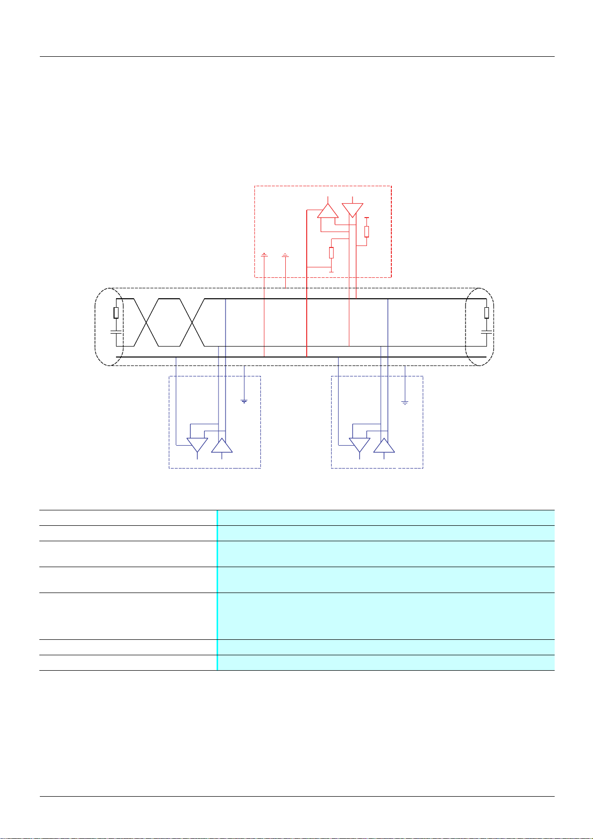
9. 2. Modbus 2-wire standard schematic
The standard schematic corresponds to the Modbus specification published in 2002 on www.modbus.org
(Modbus_over_serial_line_V1.pdf, Nov 2002) and, in particular, to the 2-wire multipoint serial bus schematic.
The Modbus card (VW3 A3 303) conforms to this specification.
Schematic diagram:
Master
G
R
650 Ω
D1
5 V
650 Ω
0 V
120 Ω
1n F
Type of trunk cable
Maximum length of bus
Maximum number of stations (without
repeater)
Maximum length of tap links
Bus polarization
Line termination
Common polarity
120 Ω
1n F
R
Slave 1
G
D0
Common
R
Slave n
G
Shielded cable with 1 twisted pair and at least a 3rd conductor
1000 m at 19200 bps with the Telemecanique TSX CSAp00 cable
32 stations, i.e., 31 slaves
• 20 m for one tap link
• 40 m divided by the number of tap links on a multiple junction box
• One 450 to 650 Ω pull-up resistor to the 5 V (650 Ω or thereabouts recommended)
• One 450 to 650
Ω pull-down resistor to the Common (650 Ω or thereabouts
recommended)
This polarization is recommended for the master.
One 120 Ω 0.25 W resistor in series with a 1nF 10 V capacitor
Yes (Common), connected to the protective ground at one or more points on the bus
40
9. Appendix
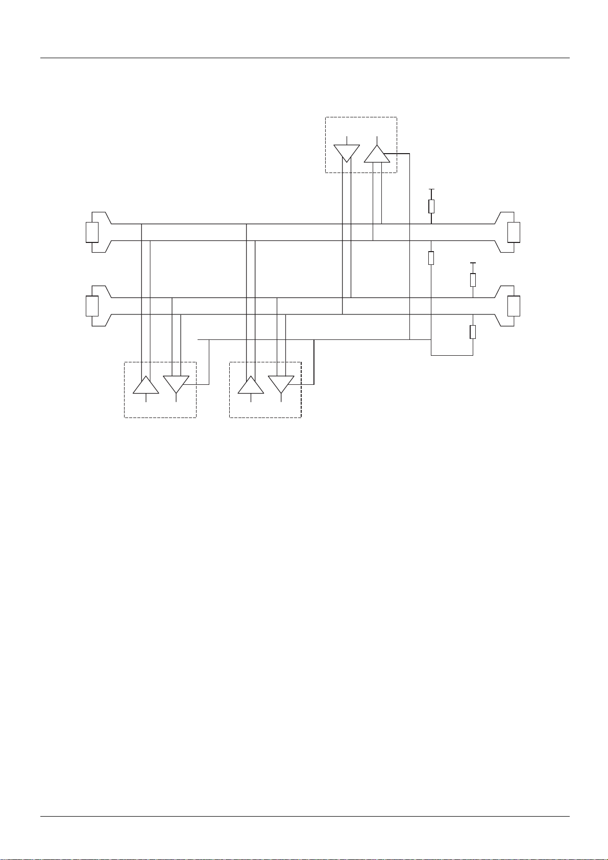
9. 3. Modbus 4-wire standard schematic
Master
G
R
5 V
TXD1
LT
TXD0
RXD1
LT
RXD0
Slave pair
Master pair
Rp
Rp
LT
5 V
Rp
LT
Rp
Common
R
G
R
G
Slave 1 Slave n
41

9. Appendix
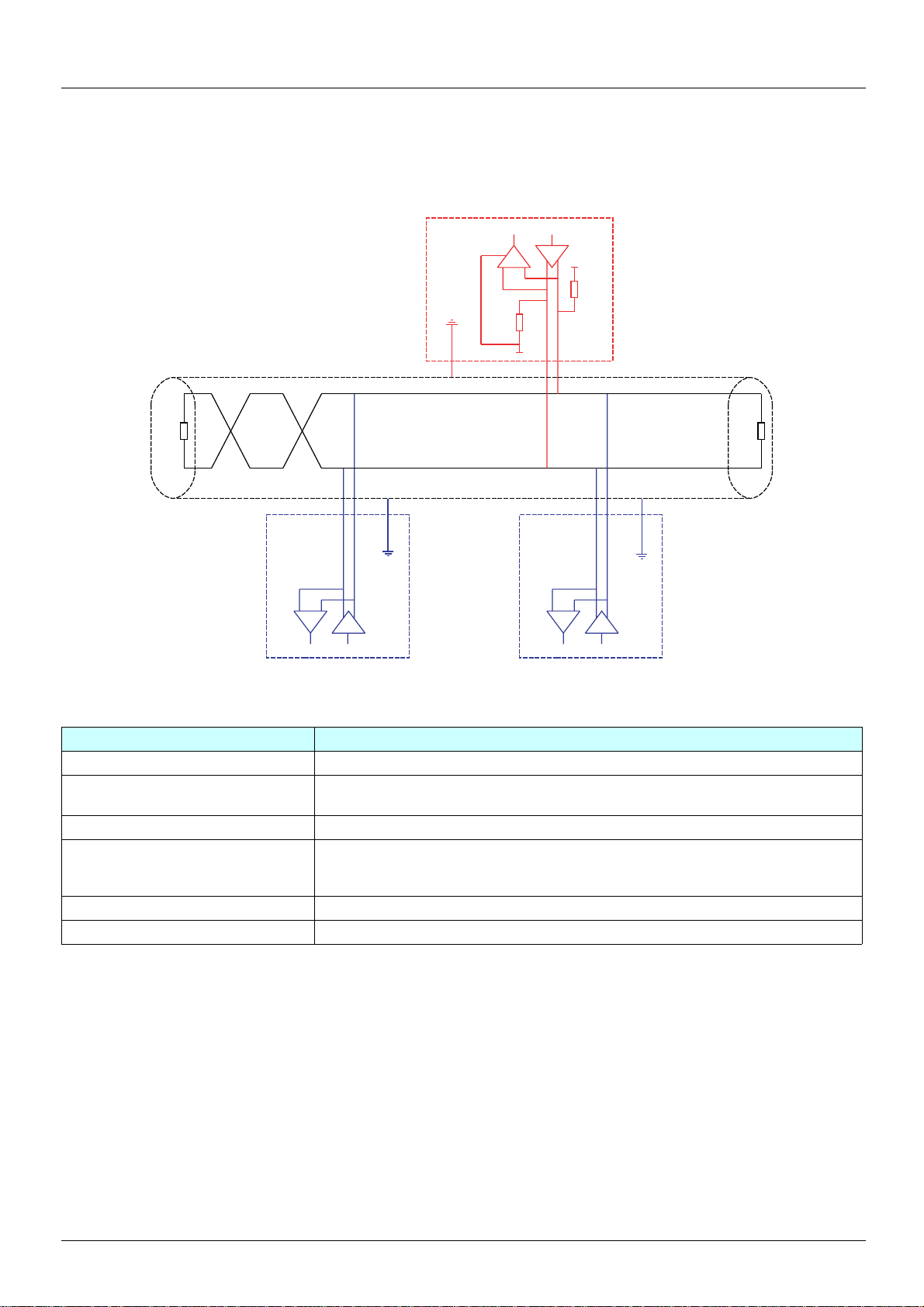
9. 4. Uni-Telway schematic
The Uni-Telway bus schematic was used by Telemecanique for older-generation drives and soft starters (ATV58, ATV28, ATS48, etc.)
marketed before the Modbus specifications were published on www.modbus.org.
Schematic diagram:
Master
G
R
4.7 kΩ
D(B)
5 V
4.7 kΩ
0 V
120 Ω
1 nF
D(A)
0VL
5 V
4.7 kΩ
0 V 0 V
R
4.7 kΩ
G
Slave 1
4.7 kΩ
R
Slave n
5 V
4.7 kΩ
G
120 Ω
1 nF
Type of trunk cable Cable with 2 twisted pairs shielded in pairs
Maximum length of bus 1000 m at 19200 bps
Maximum number of stations (without
29 stations, i.e., 28 slaves
repeater)
Maximum length of tap links
•20 m
• 40 m divided by the number of tap links on a multiple junction box
Bus polarization For the master and each slave:
• One 4.7 kΩ pull-up resistor to the 5 V
• One 4.7 kΩ pull-down resistor to the 0 VL
Line termination One 120 Ω 0.25 W resistor in series with a 1 nF 10 V capacitor
Common polarity Yes (0 VL) and high impedance placed between 0 VL and the ground in each station
42
9. Appendix
9. 5. 2-wire Jbus schematic
Schematic diagram:
150 Ω 150 Ω
L- (B/B')
L+ (A/A')
Master
470 Ω
G
R
5 V
470 Ω
0 V
R
G
Slave 1
Type of trunk cable Cable with 1 shielded twisted pair
Maximum length of bus 1,300 m at 19200 bps
Maximum number of stations (without
32 stations, i.e., 31 slaves
repeater)
Maximum length of tap links 3 m
Bus polarization One 470 Ω pull-up resistor to the 5 V
One 470 Ω pull-down resistor to the 0 V
This polarization is often provided in the master.
Line termination One 150 Ω resistor
Common polarity No
R
Slave n
G
43

9. Appendix
9. 6. Creating a Modbus bus using non-standard equipment
b Different scenarios
M If the Modbus bus is created using the latest-generation Telemecanique devices and Telemecanique Modbus wiring accessories,
installation is simple and no calculation is required (see the section entitled "Connecting to the bus").
M If a new Modbus bus has to be created using devices of different brands or older-generation devices, which do not comply with the
Modbus standard, several checks are required (see "Recommendations" below).
M If, on an existing Modbus bus, a device with 4.7 kΩ polarization is to be replaced by a new-generation device, set the 2 polarization
switches to the lower position to activate the card’s 4.7 kΩ polarization.
Polarization switche s :
Ω RS485 line polarization at drive level
4.7 k
b Recommendations
1. Identify the polarities D0 and D1.
They are labeled in different ways depending on the standard:
Standard
Modbus EIA/TIA-485
(RS 485)
D0 A/A’ D (A) RD +/TD + or L +
Signals
Generator
Receiver
However, certain RS485 electronic components are labeled in the opposite way to the EIA/TIA-485 standard.
It may be necessary to perform a test by connecting a master to a slave, then reversing the connection in the event of failure.
2. Check polarizations
Check the documentation supplied with the devices to determine their polarization.
If there is a polarization, check that the equivalent polarizat ion value is correct (see "Calculating the polarization").
It is not always possible to implement correct polarizat ion (for example, if the 5 V is not available on the master).
In this case, it may be necessary to limit the number of slaves.
3. Choose a line terminator
If there is a polarization, select an RC line terminator (R = 120 Ω, C = 1 nF)
If it is not possible to install a polarization, select an R line terminator (R = 150 Ω).
D1 B/B’ D (B) RD -/TD - or L -
Common C/C’ 0VL
BG
RR
Uni-Telway Jbus
44

9. Appendix
b Calculating the polarization
M Principle
1
1
---------
Rm
Ω and 650 Ω.
1
1
1
----------
Rs
1
---------- …+++=
Rs
1
----------
Rs
Master
R
2
---------- …+++ +=
Rs
1
2
G
5 V
You must ensure that the equivalent bus resistance is between 162
The equivalent bus resistance (Re) depends on the polarization resistance of the slaves (Rs) and the master (Rm):
1
------- -
---------
Re
Rm
If Re is too low, reduce the number of slaves.
If Re is too high, adapt the master’s polarization (if po ssible) or add polarization resistors (Rp).
1
------- -
Rp
1
------- -
Re
Rm
Rm
0 V
D1
120 Ω
1 nF
D0
5 V
Rp
Common
5 V
Rs
1
0 V
R
Slave 1
Rs
1
R
G
G
Slave n
Rp
0 V
Example 1
If the master has 470 Ω polarization and all the slaves have 4.7 kΩ polarization, a maximum of 18 slaves can be connected.
Rm = 470 Ω
Rs = 4.7 kΩ
A/Re = 1/470 + 18 x 1/4700
i.e., Re = 168 Ω
Example 2
If the bus polarization Rp is 470 Ω (installed in the master) and 2 slaves hav e 4.7 Ω polarization, the equivalent polarization is:
1/Re = 1/470 + 1/4700 + 1/4700
i.e., Re = 1/ (1/470 + 1/4700 + 1/4700)
and therefore Re = 390 Ω
390 Ω is between 162
Ω and 650 Ω, and the schematic is correct.
For an ideal equivalent polarization (650 Ω), the master’s polarization can be adapted so that:
1/650 = 1/Rm + 1/4700 + 1/4700
i.e., Rm = 1/(1/650 - 1/4700 - 1/4700)
and therefore Rm = 587 Ω
45

9. Appendix
9. 7. RS485 schematic for the card
The RS485 interface on the Modbus card is electrically isolated from the drive.
Schematic diagram:
5V
Polarization switch
Pull-up polarization resistor
4.7 k
Ω
G
Tx
D1 = B/B' = D(B)
D0 = A/A' = D(A)
Female 9-way
SUB-D
7
3
Pull-down polarization resistor
4.7 k
Enable
Ω
Polarization switch
0V
R
0V
5V
100 k
Ω
R
100 k
Ω
0V
RXD1 = RD(B)
RXD0 = RD(A)
0V
5
6
2
4
Rx
&
The polarization switches are used to connect or disconnect th e pull-up and pull-down resisto rs, which impl ement eithe r Modbus (no sla ve
polarization) or Uni-Telway (4.7 kΩ polarization for each station) type polarization.
9. 8. Card connector pinout
Contact no. Signal
1 Reserved
2RXD0 = RD(A)
3 D0 = A/A’ = D(A)
4 Common = C/C’ = 0VL
5 RxD1 = RD(B)
6 RxD1 = RD(B)
7 D1 = B/B’ = D(B)
8 Not connected
9 Not connected
46

atv71_Modbus_Jbus_EN_V1
2005-05
 Loading...