

Ordering number : ENN6266A
51003AS / D2599TH (OT) No. 6266-1/37
Overview
The LC75804E and LC75804W are 1/3 duty and 1/4 duty
LCD display drivers that can directly drive up to 300
segments and can control up to eight general-purpose
output ports. These products also incorporate a key scan
circuit that accepts input from up to 30 keys to reduce
printed circuit board wiring.
Features
• Key input function for up to 30 keys (A key scan is
performed only when a key is pressed.)
• 1/3 duty and 1/4 duty drive schemes can be controlled
from serial data.
• 1/2 bias and 1/3 bias drive schemes can be controlled
from serial data.
• Capable of driving up to 228 segments using 1/3 duty
and up to 300 segments using 1/4 duty.
• Sleep mode and all segments off functions that are
controlled from serial data.
• Segment output port/general-purpose output port
function switching that is controlled from serial data.
• Serial data I/O supports CCB format communication
with the system controller.
• Direct display of display data without the use of a
decoder provides high generality.
• Independent V
LCD
for the LCD driver block (V
LCD
can
be set to in the range VDD– 0.5 to 6.0 volts.)
• Provision of an on-chip voltage-detection type reset
circuit prevents incorrect displays.
• RES pin provided for forcibly initializing the IC internal
circuits.
• RC oscillator circuit.
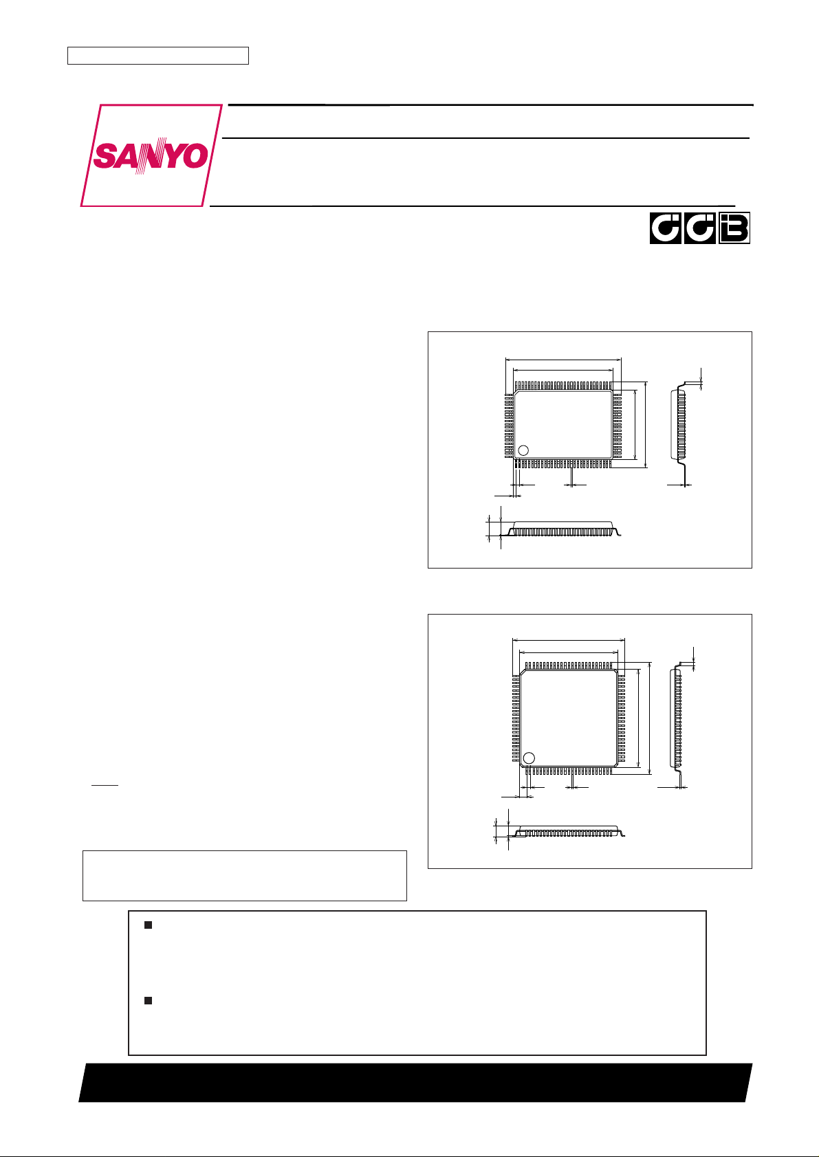
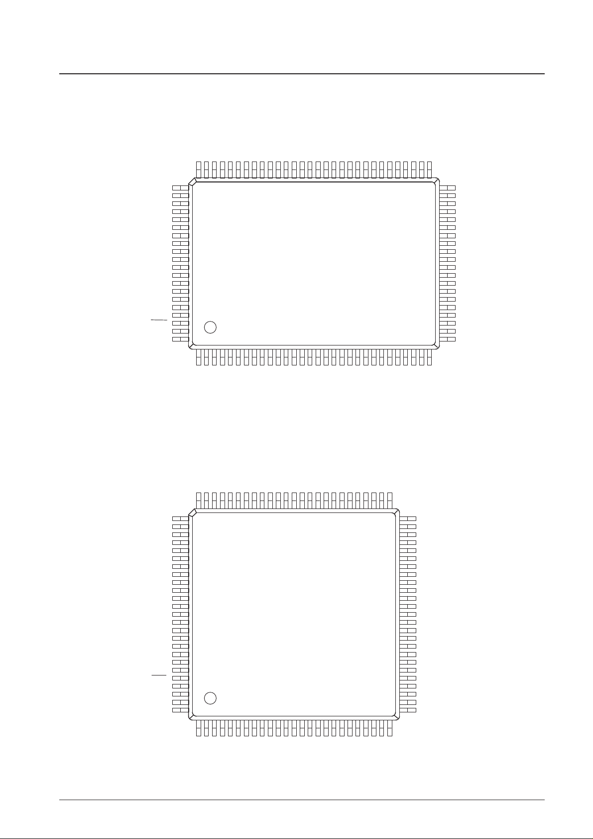
Package Dimensions
unit: mm
3151A-QFP100E
unit: mm
3181C-SQFP100
20.0
23.2
14.0
17.2
0.15
0.8
(2.7)
3.0max
0.1
0.3
0.65
(0.58)
130
80 51
31
50
100
81
SANYO: QFP100E(QIP100E)
[LC75804E]
14.0
16.0
14.0
16.0
0.145
0.2
0.5
(1.0)
(1.4)
1.6max
0.1
0.5
125
26
50
5175
76
100
SANYO: SQFP100
[LC75804W]
LC75804E, LC75804W
SANYO Electric Co.,Ltd. Semiconductor Company
TOKYO OFFICE Tokyo Bldg., 1-10, 1 Chome, Ueno, Taito-ku, TOKYO, 110-8534 JAPAN
1/3, 1/4 Duty LCD Display Drivers
with Key Input Function
CMOS IC
Any and all SANYO products described or contained herein do not have specifications that can handle
applications that require extremely high levels of reliability, such as life-support systems, aircraft’s
control systems, or other applications whose failure can be reasonably expected to result in serious
physical and/or material damage. Consult with your SANYO representative nearest you before using
any SANYO products described or contained herein in such applications.
SANYO assumes no responsibility for equipment failures that result from using products at values that
exceed, even momentarily, rated values (such as maximum ratings, operating condition ranges, or other
parameters) listed in products specifications of any and all SANYO products described or contained
herein.
• CCB is a trademark of SANYO ELECTRIC CO., LTD.
• CCB is SANYO’s original bus format and all the bus
addresses are controlled by SANYO.
No. 6266-2/37
LC75804E, LC75804W
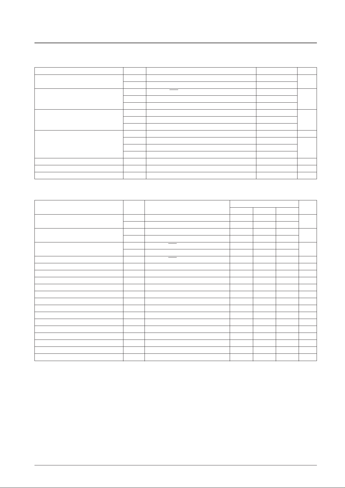
Parameter Symbol Conditions Ratings Unit
Maximum supply voltage
V
DD
max V
DD
–0.3 to +7.0 V
V
LCD
max V
LCD
–0.3 to +7.0
V
IN
1 CE, CL, DI, RES –0.3 to +7.0
Input voltage V
IN
2 OSC,TEST –0.3 to VDD+0.3 V
V
IN
3 V
LCD
1, V
LCD
2, KI1 to KI5 –0.3 to V
LCD
+0.3
V
OUT
1 DO –0.3 to +7.0
Output voltage V
OUT
2 OSC –0.3 to VDD+0.3 V
V
OUT
3 S1 to S76, COM1 to COM4, KS1 to KS6, P1 to P8 –0.3 to V
LCD
+0.3
I
OUT
1 S1 to S76 300 µA
Output current
I
OUT
2 COM1 to COM4 3
I
OUT
3 KS1 to KS6 1 mA
I
OUT
4 P1 to P8 5
Allowable power dissipation Pd max Ta = 85°C 200 mW
Operating temperature Topr –40 to +85 °C
Storage temperature Tstg –55 to +125 °C
Specifications
Absolute Maximum Ratings at Ta=25°C, VSS=0V
Parameter Symbol Conditions
Ratings
Unit
min typ max
Supply voltage
V
DDVDD
4.5 6.0
V
V
LCDVLCD
VDD– 0.5 6.0
Input voltage
V
LCD
1 V
LCD
1 2/3 V
LCD
V
LCD
V
V
LCD
2 V
LCD
2 1/3 V
LCD
V
LCD
Input high level voltage
V
IH
1 CE, CL, DI, RES 0.8 V
DD
6.0
V
V
IH
2 KI1 to KI5 0.6 V
DD
V
LCD
Input low level voltage V
IL
CE, CL, DI, RES, KI1 to KI5 0 0.2 V
DD
V
Recommended external resistance R
OSC
OSC 39 kΩ
Recommended external capacitance C
OSC
OSC 1000 pF
Guaranteed oscillator range f
OSC
OSC 19 38 76 kHz
Data setup time t
ds
CL, DI :Figure 2 160 ns
Data hold time t
dh
CL, DI :Figure 2 160 ns
CE wait time t
cp
CE, CL :Figure 2 160 ns
CE setup time t
cs
CE, CL :Figure 2 160 ns
CE hold time t
ch
CE, CL :Figure 2 160 ns
High level clock pulse width tø
H
CL :Figure 2 160 ns
Low level clock pulse width tø
L
CL :Figure 2 160 ns
Rise time t
r
CE, CL, DI :Figure 2 160 ns
Fall time t
f
CE, CL, DI :Figure 2 160 ns
DO output delay time t
dc
DO RPU=4.7 kΩ, CL=10pF *1:Figure 2 1.5 µs
DO rise time t
dr
DO RPU=4.7 kΩ, CL=10pF *1:Figure 2 1.5 µs
Allowable Operating Ranges at Ta = –40 to +85°C, VSS=0V
Note: *1. Since DO is an open-drain output, these values depend on the resistance of the pull-up resistor RPUand the load capacitance CL.
No. 6266-3/37
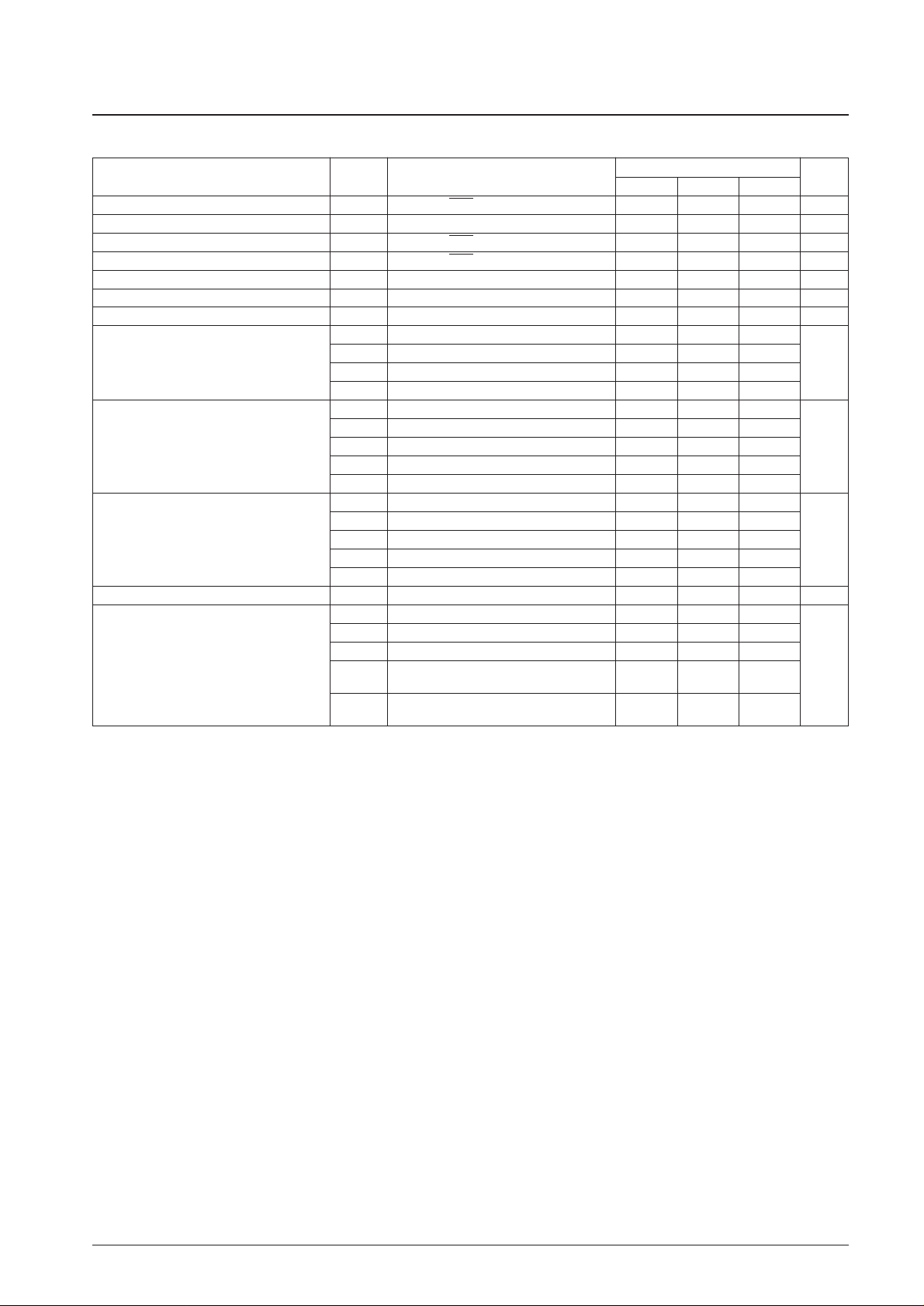
LC75804E, LC75804W
Parameter Symbol Conditions
Ratings
Unit
min typ max
Hysteresis V
H
CE, CL, DI, RES, KI1 to KI5 0.1 V
DD
V
Power-down detection voltage V
DET
2.5 3.0 3.5 V
Input high level current I
IH
CE, CL, DI, RES: VI= 6.0 V 5.0 µA
Input low level current I
IL
CE, CL, DI, RES: VI= 0 V –5.0 µA
Input floating voltage V
IF
KI1 to KI5 0.05 V
DD
V
Pull-down resistance R
PD
KI1 to KI5: VDD= 5.0 V 50 100 250 kΩ
Output off leakage current I
OFFH
DO: VO = 6.0 V 6.0 µA
V
OH
1 KS1 to KS6: IO= –500 µA V
LCD
– 1.0 V
LCD
– 0.5 V
LCD
– 0.2
Output high level voltage
V
OH
2 P1 to P8: IO= –1 mA V
LCD
– 1.0
V
V
OH
3 S1 to S76: IO= –20 µA V
LCD
– 1.0
V
OH
4 COM1 to COM4: IO= –100 µA V
LCD
– 1.0
V
OL
1 KS1 to KS6: IO= 25 µA 0.2 0.5 1.5
V
OL
2 P1 to P8: IO= 1 mA 1.0
Output low level voltage V
OL
3 S1 to S76: IO= 20 µA 1.0 V
V
OL
4 COM1 to COM4: IO= 100 µA 1.0
V
OL
5 DO: IO= 1 mA 0.1 0.5
V
MID
1 COM1 to COM4: 1/2 bias, IO= ±100 µA
1/2 V
LCD
– 1.0 1/2 V
LCD
+ 1.0
V
MID
2 S1 to S76: 1/3 bias,IO= ±20 µA
2/3 V
LCD
– 1.0 2/3 V
LCD
+ 1.0
Output middle level voltage *
2
V
MID
3 S1 to S76: 1/3 bias, IO= ±20 µA
1/3 V
LCD
– 1.0 1/3 V
LCD
+ 1.0
V
V
MID
4 COM1 to COM4: 1/3 bias,IO= ±100 µA
2/3 V
LCD
– 1.0 2/3 V
LCD
+ 1.0
V
MID
5 COM1 to COM4: 1/3 bias,IO= ±100 µA
1/3 V
LCD
– 1.0 1/3 V
LCD
+ 1.0
Oscillator frequency fosc OSC: R
OSC
= 39 kΩ, C
OSC
= 1000 pF 30.4 38 45.6 kHz
I
DD
1 VDD:Sleep mode 100
I
DD
2 VDD: VDD= 6.0 V, output open,fosc = 38 kHz 270 540
Current drain
I
LCD
1 V
LCD
: Sleep mode 5
µA
I
LCD
2
V
LCD
: V
LCD
= 6.0 V, output open, 1/2 bias,
200 400
fosc = 38 kHz
I
LCD
3
V
LCD
: V
LCD
= 6.0 V, output open, 1/3 bias,
120 240
fosc = 38 kHz
Electrical Characteristics for the Allowable Operating Ranges
Nete: *2. Excluding the bias voltage generation divider resistor built into V
LCD
1 and V
LCD
2. (See Figure 1.)
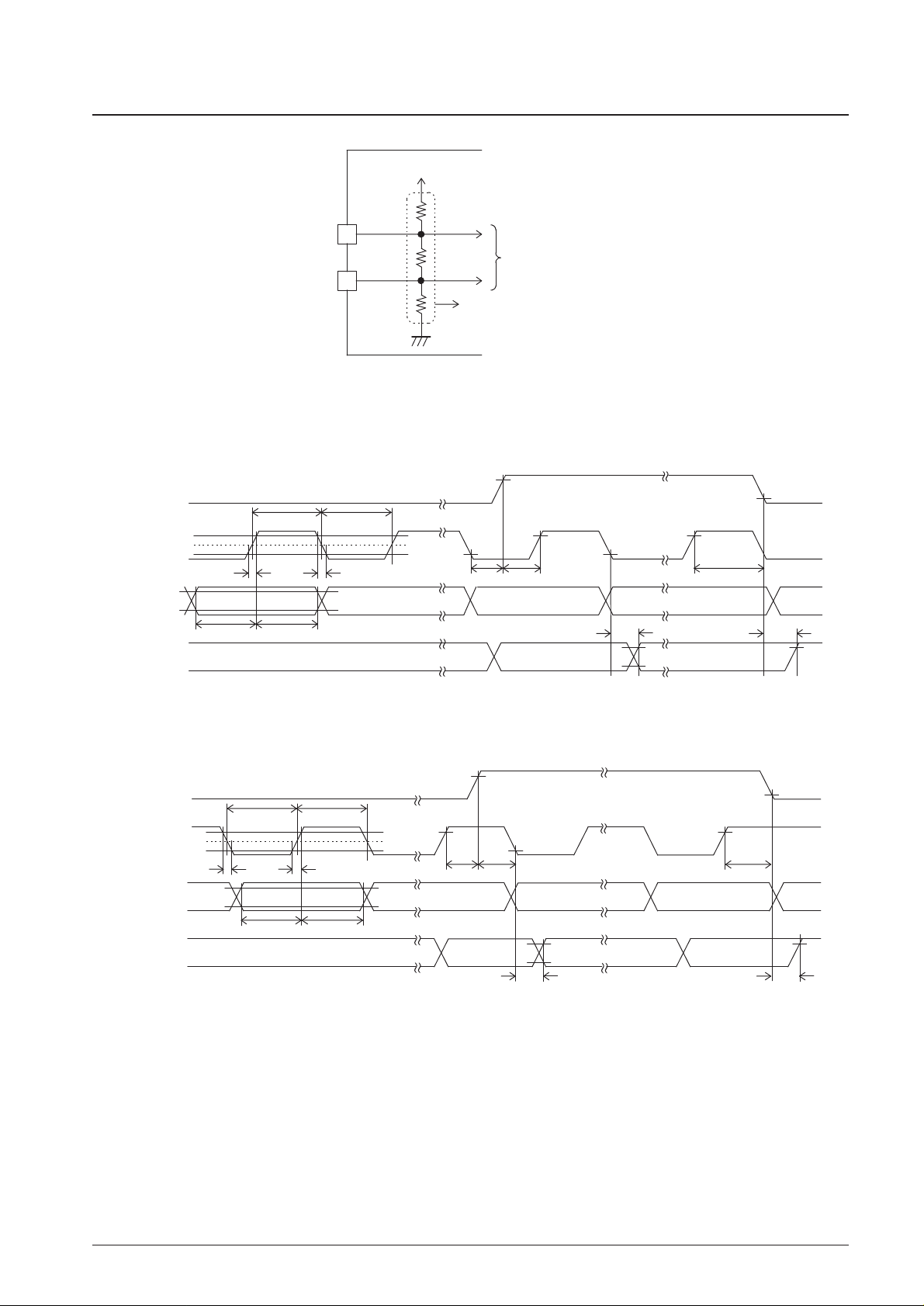
Figure 1
1. When CL is stopped at the low level
Figure 2
No. 6266-4/37
LC75804E, LC75804W
VLCD
VLCD2
V
LCD1
tdh
50%
VIH1
VIH1
VIL
VIL
VIH1
VIL
tdrtdc
tchtcstcp
tds
tr
CL
t Lt ø H
tf
DO
DI
D1D0
CE
ø
2. When CL is stopped at the high level
50%
VIH1
VIL
tdh
VIH1
VIL
VIH1
VIL
tdrtdc
tchtcstcp
tds
tf
CL
tø Htø L
tr
DO
DI
D1D0
CE
To the common segment driver
Excluding these registors.
Pin Assignments
No. 6266-5/37
LC75804E, LC75804W
KI1
VDD
VLCD2
P4/S4
S10
S16
S21
S15
S34
S39
S44
S59
S58
S49
S50
S51
S52
S53
S54
S55
S56
S57
S60
S61
S62
S63
S64
S65
S66
S67
S68
S69
S70
S71
S72
S73
COM4/S74
COM3
COM2
COM1
KS1/S75
P3/S3
S9
P2/S2
P1/S1
DI
CL
LC75804E
(QFP100E)
S76/KS2
KS6
KS3
KS4
KS5
KI2
KI3
KI5
KI4
VLCD
VLCD1
VSS
TEST
RES
OSC
DO
S33
S32
S31
S30
S29CE
5180
5081
31100
30
(Top view)
(Top view)
1
P8/S8
P7/S7
P6/S6
P5/S5
S14
S20
S13
S12
S11
S19
S18
S17
S25
S24
S23
S22
S28
S27
S26
S38
S37
S36
S35
S43
S42
S41
S40
S48
S47
S46
S45
S55
S51
S52
S53
S54
S56
S57
S58
S59
S60
S61
S62
S63
S64
S65
S66
S67
S68
S69
S70
S71
S72
S73
COM4/S74
COM3
P5/S5
S11
P4/S4
P3/S3
P2/S2
P1/S1
LC75804W
(SQFP100)
COM1
S76/KS2
S75/KS1
KS3
COM2
KS4
KS5
KS6
KI2
KI1
KI4
KI3
S35
S34
S33
S32
S31
S29
S30
S27
S28
S26DI
5175
5076
26100
251
KI5
VLCD
VDD
VLCD2
VLCD1
VSS
OSC
TEST
RES
CE
DO
CL
S10
S9
P8/S8
P7/S7
P6/S6
S16
S22
S15
S14
S13
S12
S21
S20
S19
S18
S17
S25
S24
S23
S40
S39
S38
S37
S36
S45
S44
S43
S42
S41
S50
S49
S48
S47
S46
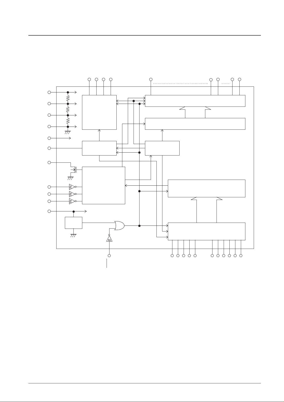
Block Diagram
No. 6266-6/37
LC75804E, LC75804W
VDET
CCB
INTERFACE
COM4/S74
COM3
COM2
COM1
COMMON
DRIVER
CLOCK
GENERATOR
VSS
VLCD2
VLCD1
VLCD
CE
VDD
DI
TEST
CL
DO
OSC
RES
KI5
KI4
KI3
KI2
KI1
KS6
KS5
KS4
KS3
S76/KS2
S75/KS1
KEY SCAN
KEY BUFFER
CONTROL
REGISTER
SHIFT REGISTER
SEGMENT DRIVER & LATCH
S1/P1
S2/P2
S8/P8
S9
S73

No. 6266-7/37
LC75804E, LC75804W
Pin
Pin No.
Function Active I/O
Handling
LC75804E LC75804W
when unused
—
●● OPEN
COM1
COM2
— ●● OPEN
COM3
COM4/S74
KS1/S75 80 78
KS2/S76 81 79 — O OPEN
KS3 to KS6 82 to 85 80 to 83
KI1 to KI5 86 to 90 84 to 88 H I GND
OSC 97 95 — I/O V
DD
CE 100 98 H I
CL 1 99 I GND
DI 2 100 — I
DO 99 97 — O OPEN
RES 98 96 L I V
DD
TEST 96 94 This pin must be connected to ground. — I —
V
LCD
1 93 91 — I OPEN
V
LCD
2 94 92 — I OPEN
V
DD
91 89 — — —
V
LCD
92 90 — — —
V
SS
95 93 Power supply connection. Connect to ground. — — —
Pin Functions
Segment outputs for displaying the display data transferred by serial
data input.
The S1/P1 to S8/P8 pins can be used as general-purpose output ports
under serial data control.
Common driver outputs
The frame frequency fo is given by : fo = (f
OSC
/384)Hz.
The COM4/S74 pin can be used as a segment output in 1/3 duty.
Key scan outputs
Although normal key scan timing lines require diodes to be inserted in
the timing lines to prevent shorts, since these outputs are unbalanced
CMOS transistor outputs, these outputs will not be damaged by shorting
when these outputs are used to form a key matrix. The KS1/S75 and
KS2/S76 pins can be used as segment outputs when so specified by
the control data.
Key scan inputs
These pins have built-in pull-down resistors.
Oscillator connection
An oscillator circuit is formed by connecting an external resistor and
capacitor at this pin.
Serial data interface connections to the controller. Note that DO, being
an open-drain output, requires a pull-up resistor.
CE :Chip enable
CL :Synchronization clock
DI :Transfer data
DO :Output data
▲
Reset signal input
RES = low
.....
Display off
Key scan disabled
All key data is reset to low
RES = high
....
Display on
Key scan enabled
However, serial data can be transferred when RES is low.
Used for applying the LCD drive 2/3 bias voltage externally. Must be
connected to V
LCD
2 when a 1/2 bias drive scheme is used.
Used for applying the LCD drive 1/3 bias voltage externally. Must be
connected to V
LCD
1 when a 1/2 bias drive scheme is used.
Logic block power supply connection. Provide a voltage of between 4.5
and 6.0V.
LCD driver block power supply connection. Provide a voltage of
between V
DD
– 0.5 and 6.0V.
S1/P1 to
S8/P8
S9 to S73
3 to 10
11 to 75
1 to 8
9 to 73
79
78
77
76
77
76
75
74
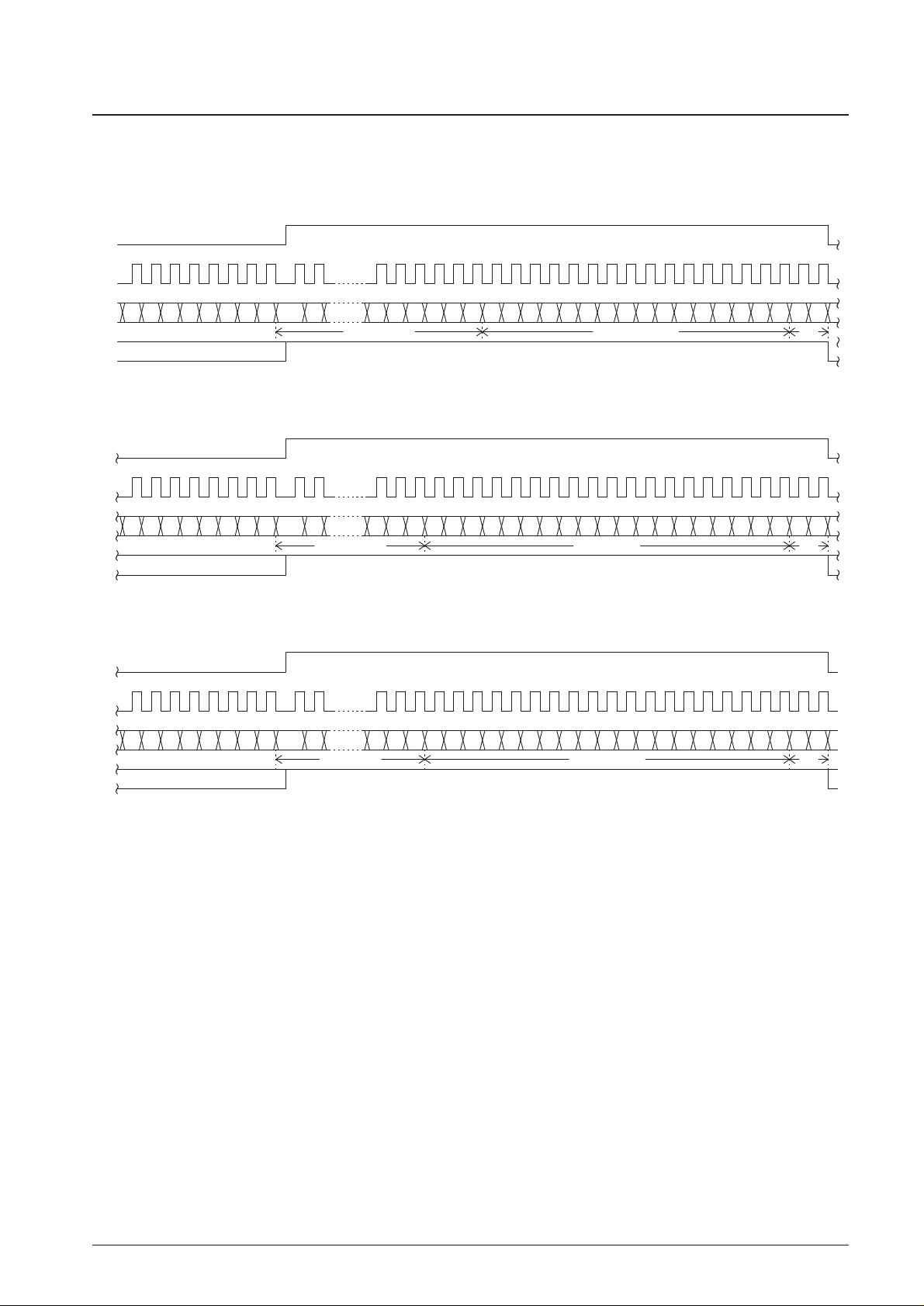
Serial Data Input
1. 1/3 duty
① When CL is stopped at the low level
Note: B0 to B3, A0 to A3
......
CCB address
DD
................................
Direction data
No. 6266-8/37
LC75804E, LC75804W
A3A2A1A0B3B2B1B0
00
DRSC
P3P2P1P0K1K0S1S0 DT000
D78D77D76D75D74D73D2D1
01000010
DD
DO
DI
CL
CE
00
A3A2A1A0B3B2B1B0
1000000000000000
D153D152D151D80D79
01000010
DD
00000
A3A2A1A0B3B2B1B0
0100000000000000
D228D227D226D155D154
01000010
DD
00000
Display data Control data
Fixed data
Display data
Fixed data
Display data

No. 6266-9/37
LC75804E, LC75804W
② When CL is stopped at the high level
Note: B0 to B3, A0 to A3
......
CCB address
DD
................................
Direction data
CCB address
............
42H
D1 to D228
..............
Display data
S0, S1
......................
Sleep control data
K0, K1
......................
Key scan output/segment output selection data
P0 to P3
..................
Segment output port/general-purpose output port selection data
SC
............................
Segment on/off control data
DR
............................
1/2 bias or 1/3 bias drive selection data
DT
............................
1/3 duty or 1/4 duty drive selection data
A3A2A1A0B3B2B1B0
00
DT
DRSCP3P2P1P0K1K0S1S0000
D78D77D76D75D74D73D2D1
01000010
DD
DO
DI
CL
CE
00
A3A2A1A0B3B2B1B0
1000000000000000
D153D152D151D80D79
01000010
DD
00000
A3A2A1A0B3B2B1B0
0100000000000000
D228D227D226D155D154
01000010
DD
00000
Display data
Control data
Fixed data
Display data
Display data
Fixed data

No. 6266-10/37
LC75804E, LC75804W
2. 1/4duty
① When CL is stopped at the low level
Note: B0 to B3, A0 to A3
......
CCB address
DD
................................
Direction data
A3A2A1A0B3B2B1B0
00DRSCP3P2P1P0K1K0S1S0 DT000
D76D75D74D72 D73D1
01000010
DD
DO
DI
CL
CE
0000
A3A2A1A0B3B2B1B0
1000000000000000
D152D151D150D148 D149 D77
01000010
DD
0000
A3A2A1A0B3B2B1B0
0100000000000000
D228D227D226D224 D225D153
01000010
DD
0000
A3A2A1A0B3B2B1B0
110000000000000001000010
DD
00000
D300
D229
000
Display data
Control data
Fixed data
Display data
Display data
Display data
Fixed data
Fixed data

No. 6266-11/37
LC75804E, LC75804W
② When CL is stopped at the high level
Note: B0 to B3, A0 to A3
......
CCB address
DD
................................
Direction data
CCB address
............
42H
D1 to D300
..............
Display data
S0, S1
......................
Sleep control data
K0, K1
......................
Key scan output/segment output selection data
P0 to P3
..................
Segment output port/general-purpose output port selection data
SC
............................
Segment on/off control data
DR
............................
1/2 bias or 1/3 bias drive selection data
DT
............................
1/3 duty or 1/4 duty drive selection data
A3A2A1A0B3B2B1B0
00DTDRSCP3P2P1P0K1K0S1S0
000
D76D75D74D72 D73
D1
01000010
DD
DO
DI
CL
CE
0000
A3A2A1A0B3B2B1B0
1000000000000000
D152D151D150D148 D149
D77
01000010
DD
0000
A3A2A1A0B3B2B1B0
0100000000000000
D228D227D226D224 D225
D153
01000010
DD
0000
A3A2A1A0B3B2B1B0
1100000000000000
D300D229
01000010
DD
00000000
Display data
Control data
Fixed data
Display data
Display data
Display data
Fixed data
Fixed data
Control Data Functions
1. S0, S1 : Sleep control data
These control data bits switch between normal mode and sleep mode and set the states of the KS1 to KS6 key scan
outputs during key scan standby.
Note: This assumes that the KS1/S75 and KS2/S76 output pins are selected for key scan output.
No. 6266-12/37
LC75804E, LC75804W
Control data
Mode OSC oscillator
Segment outputs
Output pin states during key scan standby
S0 S1
Common outputs
KS1 KS2 KS3 KS4 KS5 KS6
0 0 Normal Operating Operating H H H H H H
0 1 Sleep Stopped L L L L L L H
1 0 Sleep Stopped L L L L L H H
1 1 Sleep Stopped L H H H H H H
2. K0, K1 : Key scan output /segment output selection data
These control data bits switch the functions of the KS1/S75 and KS2/S76 output pins between key scan output and
segment output.
X: don’t care
Note: KSn(n = 1 or 2) : Key scan output
Sn (n = 75 or 76): Segment output
Control data Output pin state
Maximum number of
K0 K1 KS1/S75 KS2/S76
input keys
0 0 KS1 KS2 30
0 1 S75 KS2 25
1 X S75 S76 20
3. P0 to P3 : Segment output port/general-purpose output port selection data
These control data bits switch the functions of the S1/P1 to S8/P8 output pins between the segment output port and
the general-purpose output port.
Note: Sn(n=1 to 8): Segment output port
Pn(n=1 to 8): General-purpose output port
The table below lists the correspondence between the display data and the output pins when these pins are selected to
be general-purpose output ports.
For example, if the circuit is operated in 1/4 duty and the S4/P4 output pin is selected to be a general-purpose output
port, the S4/P4 output pin will output a high level (V
LCD
) when the display data D13 is 1, and will output a low level
(Vss) when D13 is 0.
Control data Output pin state
P0 P1 P2 P3 S1/P1 S2/P2 S3/P3 S4/P4 S5/P5 S6/P6 S7/P7 S8/P8
0 0 0 0 S1 S2 S3 S4 S5 S6 S7 S8
0 0 0 1 P1 S2 S3 S4 S5 S6 S7 S8
0 0 1 0 P1 P2 S3 S4 S5 S6 S7 S8
0 0 1 1 P1 P2 P3 S4 S5 S6 S7 S8
0 1 0 0 P1 P2 P3 P4 S5 S6 S7 S8
0 1 0 1 P1 P2 P3 P4 P5 S6 S7 S8
0 1 1 0 P1 P2 P3 P4 P5 P6 S7 S8
0 1 1 1 P1 P2 P3 P4 P5 P6 P7 S8
1 0 0 0 P1 P2 P3 P4 P5 P6 P7 P8
Output pin
Corresponding display data
1/3 duty 1/4 duty
S1/P1 D1 D1
S2/P2 D4 D5
S3/P3 D7 D9
S4/P4 D10 D13
S5/P5 D13 D17
S6/P6 D16 D21
S7/P7 D19 D25
S8/P8 D22 D29
 Loading...