

SANYO LC7574NW, LC7574NE Datasheet
Ordering number : EN3586A
SANYO Electric Co.,Ltd. Semiconductor Bussiness Headquarters
TOKYO OFFICE Tokyo Bldg., 1-10, 1 Chome, Ueno, Taito-ku, TOKYO, 110-8534 JAPAN
CMOS LSI
O2095HA (OT)/4032JN No. 3586-1/10
Overview
The LC7574NE and LC7574NW are 1/2 duty VFD
drivers that can be used for electronic tuning frequency
display and other applications under the control of a
controller. These products can directly drive VFDs with
up to 74 segments.
Features
• 74 segment outputs
• Noise reduction circuits are built into the output drivers.
• Serial data input supports CCB* format
communications with the system controller.
• Switching between digital and analog dimmers under
serial data control
• High generality since display data is displayed without
the intervention of a decoder
• All segments can be turned off with the BLK pin
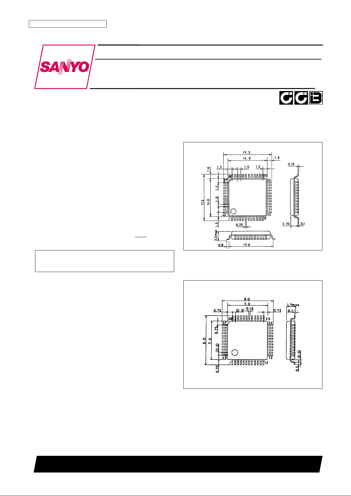
Package Dimensions
unit: mm
3156-QFP48E
SANYO: QFP48E
[LC7574NE]
unit: mm
3163A-SQFP48
SANYO: SQFP48
[LC7574NW]
• CCB is a trademark of SANYO ELECTRIC CO., LTD.
• CCB is SANYO’s original bus format and all the bus
addresses are controlled by SANYO.
1/2 Duty VFD Driver for Frequency Display
LC7574NE, 7574NW

Specifications
Absolute Maximum Ratings at Ta = 25°C, VSS= 0 V
Allowable Operating Ranges at Ta = –40 to +85°C, VDD= 4.5 to 5.5 V, VSS= 0 V
Electrical Characteristics in the Allowable Operating Ranges
No. 3586-2/10
LC7574NE, 7574NW
Parameter Symbol Conditions Ratings Unit
Maximum supply voltage
V
DD
max V
DD
–0.3 to +6.5 V
V
FL
max V
FL
–0.3 to +21.0 V
Input voltage
V
IN
1 DI, CL, CE, BLK, DIM –0.3 to +6.5 V
V
IN
2 OSC –0.3 to VDD+ 0.3 V
Output voltage
V
OUT
1 S1 to S37, G1, G2 –0.3 to VFL+ 0.3 V
V
OUT
2 OSC –0.3 to VDD+ 0.3 V
Output current
I
OUT
1 S1 to S37 5 mA
I
OUT
2 G1, G2 67 mA
Allowable power dissipation Pd max
Ta = 85°C (LC7574NE) 250 mW
Ta = 85°C (LC7574NW) 150 mW
Operating temperature Topr –40 to +85 °C
Storage temperature Tstg –50 to +125 °C
Parameter Symbol Conditions min typ max Unit
Supply voltage
V
DD
V
DD
4.5 5.0 5.5 V
V
FL
V
FL
8 12 18 V
Input high level voltage V
IH
DI, CL, CE, BLK 0.8 V
DD
5.5 V
Input low level voltage V
IL
DI, CL, CE, BLK 0 0.2 V
DD
V
Guaranteed oscillator range f
OSC
OSC 0.4 1.6 3.0 MHz
Recommended external
R
OSC
OSC 12 kΩ
resistance
Recommended external
C
OSC
OSC 50 pF
capacitance
Low level clock pulse width t
øL
CL: Figure 1 0.5 µs
High level clock pulse width t
øH
CL: Figure 1 0.5 µs
Data setup time t
ds
DI, CL: Figure 1 0.5 µs
Data hold time t
dh
DI, CL: Figure 1 0.5 µs
CE wait time t
cp
CE, CL: Figure 1 0.5 µs
CE setup time t
cs
CE, CL: Figure 1 0.5 µs
CE hold time t
ch
CE, CL: Figure 1 0.5 µs
BLK switching time t
c
BLK, CE: Figure 3 10 µs
Input voltage range V
IN
DIM 0 +5.5 V
Parameter Symbol Conditions min typ max Unit
Input high level current I
IH
DI, CL, CE, BLK, DIM: VI= 5.5 V 5 µA
Input low level current I
IL
DI, CL, CE, BLK, DIM: VI= 0 V –5 µA
V
OH
1 S1 to S37: IO= 2 mA VFL– 0.6 V
Output high level voltage V
OH
2 G1, G2: IO= 25 mA VFL– 0.6 V
V
OH
3 G1, G2: IO= 50 mA VFL– 1.3 V
Output low level voltage V
OL
S1 to S37, G1, G2: IO= –5 µA, Ta = 25°C 0.125 0.25 0.5 V
Oscillator frequency f
OSC
R
OSC
= 12 kΩ, C
OSC
= 50 pF 1.6 MHz
Hysteresis voltage V
H
DI, CL, CE, BLK 0.5 V
A/D converter linearity error Err DIM –1/2 +1/2 LSB
Current drain I
DD
Outputs open: f
OSC
= 1.6 MHz 10 mA

Pin Assignment
1. When CL is stopped at the low level
2. When CL is stopped at the high level
Figure 1
No. 3586-3/10
LC7574NE, 7574NW
 Loading...