


CMOS LSI
Ordering number : EN4922C
73096HA (OT)/11095TH (OT) No. 4922-1/21
SANYO Electric Co.,Ltd. Semiconductor Bussiness Headquarters
TOKYO OFFICE Tokyo Bldg., 1-10, 1 Chome, Ueno, Taito-ku, TOKYO, 110 JAPAN
PLL Frequency Synthesizer
for Electronic Tuning
LC72146, 72146M
Overview
The LC72146 is a PLL frequency synthesizer LSI circuit
for electronic tuning in car stereo systems. The LC72146
supports the construction of high-performance, multifunctional electronic tuning systems for the VHF MW,
and LW bands.
Features
• High-speed programmable dividers for
— 10 to 160 MHz on FMIN using pulse swallower
— 0.5 to 40.0 MHz on AMIN using pulse swallower
and direct division
• General-purpose counters
— HCTR for 0.4 to 25.0 MHz frequency measurement
— LCTR for 10 to 500 kHz frequency measurement
and 1.0 Hz to 20 × 103kHz period measurement
• Reference frequencies: Twelve selectable reference
frequencies (4.5 or 7.2 MHz crystal) 1, 3, 5, 9, 10,
3.125, 6.25, 12.5, 25, 30, 50 and 100 kHz
• Phase comparator
— Insensitive band control
— Unlock detection
— Sub-charge pump for high-speed locking
— Deadlock clear circuit
• CCB input/output data interface
• Power-on reset circuit
• Built-in MOS transistor for a low-pass filter
• Inputs/outputs (using five general-purpose input/output
ports)
— Maximum of seven inputs (max)
— Maximum of seven outputs (max/four n-channel
open-drain and three CMOS outputs)
— Time-base output for clock (8 Hz)
• Operating ranges
— Supply voltage ..................................4.5 to 5.5 V
— Opetating temperature ......................–40 to 85°C
• Package
— DIP24S, MFP24S
Package Dimensions
unit: mm
3067-DIP24S
unit: mm
3112-MFP24S
SANYO: DIP24S
[LC72146]
SANYO: MFP24S
[LC72146M]
• CCB is a trademark of SANYO ELECTRIC CO., LTD.
• CCB is SANYO’s original bus format and all the bus
addresses are controlled by SANYO.
Specifications
Absolute Maximum Ratings at Ta = 25°C, VSS= 0 V
Allowable Operating Ranges at Ta = –40 to 85°C, VSS= 0 V
No. 4922-2/21
LC72146, 72146M
Parameter Symbol Conditions min typ max Unit
Supply voltage
V
DD
1 V
DD
4.5 5.5 V
V
DD
2 VDD: Serial data retain voltage 2.0 V
Input high-level voltage
V
IH
1 CE, CL, DI, I/O-1 to I/O-3 2.2 6.5 V
V
IH
2 I/O-4, I/O-5, HCTR/I-6 and LCTR/I-7 2.2 V
DD
V
Input low-level voltage V
IL
1 CE, CL, DI and I/O-1 to I/O-5, HCTR/I-6, LCTR/I-7 0 0.8 V
Input high-leve lvoltage V
IH
3 LCTR/I-7, Pulse wave
*1
2.2 V
DD
V
Input low-level voltage V
IL
2 LCTR/I-7, Pulse wave
*1
0 0.8 V
Output voltage
V
O
1 DO 0 6.5 V
V
O
2 I/O-1 to I/O-3, AOUT, O-7 0 13 V
f
IN
1 XIN; Sine wave, capacitive coupling 1.0 8.0 MHz
f
IN
2 FMIN; Sine wave, capacitive coupling 10 160 MHz
Input frequency
f
IN
3 AMIN; Sine wave, capacitive coupling 0.5 40 MHz
f
IN
4 HCTR/I-6; Sine wave, capacitive coupling 0.4 25 MHz
f
IN
5 LCTR/I-7; Sine wave, capacitive coupling 10 500 kHz
f
IN
6 LCTR/I-7; Pulse wave, DC coupling
*1
1.0 20 × 10
3
Hz
Guaranteed oscillator
Xtal XIN, XOUT; CI ≤ 120 Ω 4.0 8.0 MHz
element frequencies
V
IN
1 XIN 200 1500 mVrms
V
IN
2-1 FMIN; 50 ≤ f < 130 MHz
*2
40 1500 mVrms
V
IN
2-2 FMIN; 10 ≤ f < 50 MHz*2, 130 ≤ f 160 MHz 70 1500 mVrms
V
IN
3-1 AMIN; 2 ≤ f < 25 MHz
*2
40 1500 mVrms
V
IN
3-2 AMIN; 25 ≤ f < 40 MHz
*2
70 1500 mVrms
V
IN
3-3 AMIN; 0.5 ≤ f < 2.5 MHz
*2
40 1500 mVrms
Input amplitude
V
IN
3-4 AMIN; 2.5 ≤ f < 10 MHz
*2
70 1500 mVrms
V
IN
4-1 HCTR/I-6; 0.4 ≤ f < 25 MHz
*3
40 1500 mVrms
V
IN
4-2 HCTR/I-6; 8 ≤ f < 12 MHz
*4
70 1500 mVrms
V
IN
5-1 LCTR/I-7; 10 ≤ f < 400 kHz
*3
40 1500 mVrms
V
IN
5-2 LCTR/I-7; 400 ≤ f < 500 kHz
*3
20 1500 mVrms
V
IN
5-3 LCTR/I-7; 400 ≤ f < 500 kHz
*4
70 1500 mVrms
Data set up time t
SU
DI, CL
*5
0.45 µS
Data hold time t
HD
DI, CL
*5
0.45 µS
Parameter Symbol Conditions Ratings Unit
Maximum supply voltage V
DD
max V
DD
–0.3 to +7.0 V
V
IN
1 max CE, CL, DI –0.3 to +7.0 V
Maximum input voltage V
IN
2 max XIN, FMIN, AIN, AMIN, HCTR/I-6, LCTR/I-7, I/O-4, I/O-5 –0.3 to VDD+ 0.3 V
V
IN
3 max I/O-1 to I/O-3 –0.3 to +15 V
V
O
1 max DO –0.3 to +7.0 V
Maximum output voltage V
O
2 max XOUT, I/O-4, I/O-5, O-6, PD0, PF1, AIN –0.3 to VDD+ 0.3 V
V
O
3 max I/O-1 to I/O-3, AOUT, O-7 –0.3 to +15 V
I
O
1 max I/O-4, I/O-5, O-6, O-7 0 to 3.0 mA
Maximum output current I
O
2 max DO, AOUT 0 to 6.0 mA
I
O
3 max I/O-1 to I/O-3 0 to 10 mA
Allowable power dissipation Pd max
DIP24S:Ta ≤ 85°C 350 mW
MFP24S:Ta ≤ 85°C 220 mW
Operating temperature Topr –40 to +85 °C
Storage temperature Tstg –55 to +125 °C
Continued on next page.
Continued from preceding page.
Note: 1. Period measurement
2. See the description of the structure of the programmable divider.
3. With the CTC bit in the serial data set to 0
4. With the CTC bit in the serial data set to 1
5. See the description of the serial data timing.
Electrical Characteristics at Ta = –40 to +85°C, VSS= 0 V
No. 4922-3/21
LC72146, 72146M
Parameter Symbol Conditions min typ max Unit
Clock low-level time t
CL
CL
*5
0.45 µs
Clock high-level time t
CH
CL
*5
0.45 µs
CE wait time t
EL
CE, CL
*5
0.45 µs
CE setup time t
ES
CL, CE
*5
0.45 µs
CE hold time t
EH
CE, CL
*5
0.45 µs
Chip enable to data latch time t
LC
*5
0.45 µs
Data output time t
DC
DO, CL; Depends on pull-up resistor 0.2 µs
Parameter Symbol Conditions min typ max Unit
Rf1 XIN 1.0 mΩ
Rf2 FMIN 500 kΩ
Internal feedback resistance Rf3 AMIN 500 kΩ
Rf4 HCTR/I-6 250 kΩ
Rf5 LCTR/I-7 250 kΩ
Sub charge pump
R1S AIN 100 Ω
internal resistance
Hysteresis V
HIS
CE, CL, DI, LCTR/I-7 0.1 V
DD
V
I
O
= 0.5 mA VDD– 0.5 V
Output high-level voltage
V
OH
1 PD0, PD1, I/O-4, I/O-5, O-6 IO= 1 mA VDD– 1.0 V
I
O
= 2 mA VDD– 2.0 V
V
OH
2 AIN: IO= 1 mA VDD– 0.6 VDD– 0.3 V
I
O
= 0.5 mA 0.5 V
V
OL
1
PD0, PD1, I/O-4,
IO= 1 mA 1.0 V
I/O-5, O-6, O-7
I
O
= 2 mA 2.0 V
V
OL
2 AIN: IO= 1 mA 0.3 0.6 V
Output low-level voltage
I
O
= 1 mA 0.2 V
V
OL
3 I/O-1 to I/O-3
I
O
= 2.5 mA 0.5 V
I
O
= 5 mA 1.0 V
I
O
= 9 mA 1.8 V
V
OL
4 DO; IO= 5 mA 1.0 V
V
OL
5 AOUT; IO= 1 mA, AIN = 1.3 V 0.5 V
I
IH
1 CE, CL, DI; VI= 6.5 V 5.0 µA
I
IH
2 I/O-1 to I/O-3; VI= 13 V 5.0 µA
Input high-level current
I
IH
3 I/O-4, I/O-5, HCTR/I-6, LCTR/I-7; VI= V
DD
5.0 µA
I
IH
4 XIN; VI= V
DD
2.0 11 µA
I
IH
5 FMIN, AMIN; VI= V
DD
4.0 22 µA
I
IH
6 HCTR/I-6, LCTR/I-7; VI= V
DD
8.0 44 µA
I
IL
1 CE, CL, DI; VI= 0 V 5.0 µA
I
IL
2 I/O-1 to I/O5; VI= 0 V 5.0 µA
Input low-level current
I
IL
3 HCTR/I-6, LCTR/I-7; VI= 0 V 5.0 µA
I
IL
4 XIN; VI= 0 V 2.0 11 µA
I
IL
5 FMIN, AMIN; VI= 0 V 4.0 22 µA
I
IL
6 HCTR/I-6, LCTR/I-7; VI= 0 V 8.0 44 µA
Continued on next page.

Continued from preceding page.
Pin Assignment
Block Diagram
No. 4922-4/21
LC72146, 72146M
Parameter Symbol Conditions min typ max Unit
Output off leakage current
I
OFF
1 I/O-1 to I/O3, AOUT, O-7; VO= 13 V 5.0 µA
I
OFF
2 DO; VO= 6.5 V 5.0 µA
High-level three state
I
OFFH
PD0, PD1, AIN; VO= V
DD
0.01 200 nA
off leakage current
Lowh-level three state
I
OFFL
PD0, PD1, AIN; VO= 0 V 0.01 200 nA
off leakage current
Input cacitance C
IN
FMIN 6 pF
Pull-down transistor
R
pd
1 FMIN 80 200 600 kΩ
on resistance
R
pd
2 AMIN 80 200 600 kΩ
V
DD
; Xtal = 7.2 MHz, fIN2 = 160 MHz,
I
DD
1 VIN2 = 70 mVrms, fIN4 = 25 MHz 10 15 mA
Supply current
V
IN
4 = 40 mVrms
I
DD
2
V
DD
; PLL inhibited,
0.5 1.5 mA
crystal oscillator running (Xtal = 7.2 MHz)
I
DD
3 VDD;PLL inhibited, crystal oscillator stoped 10 µA
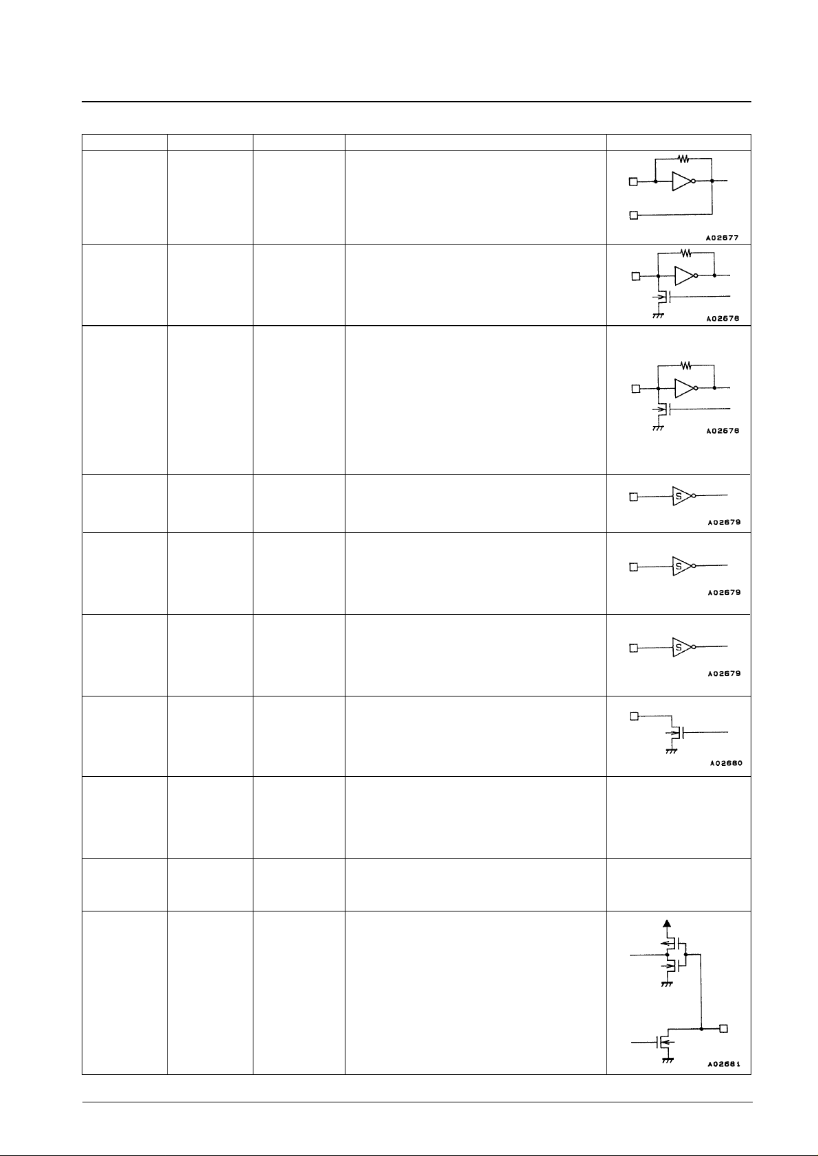
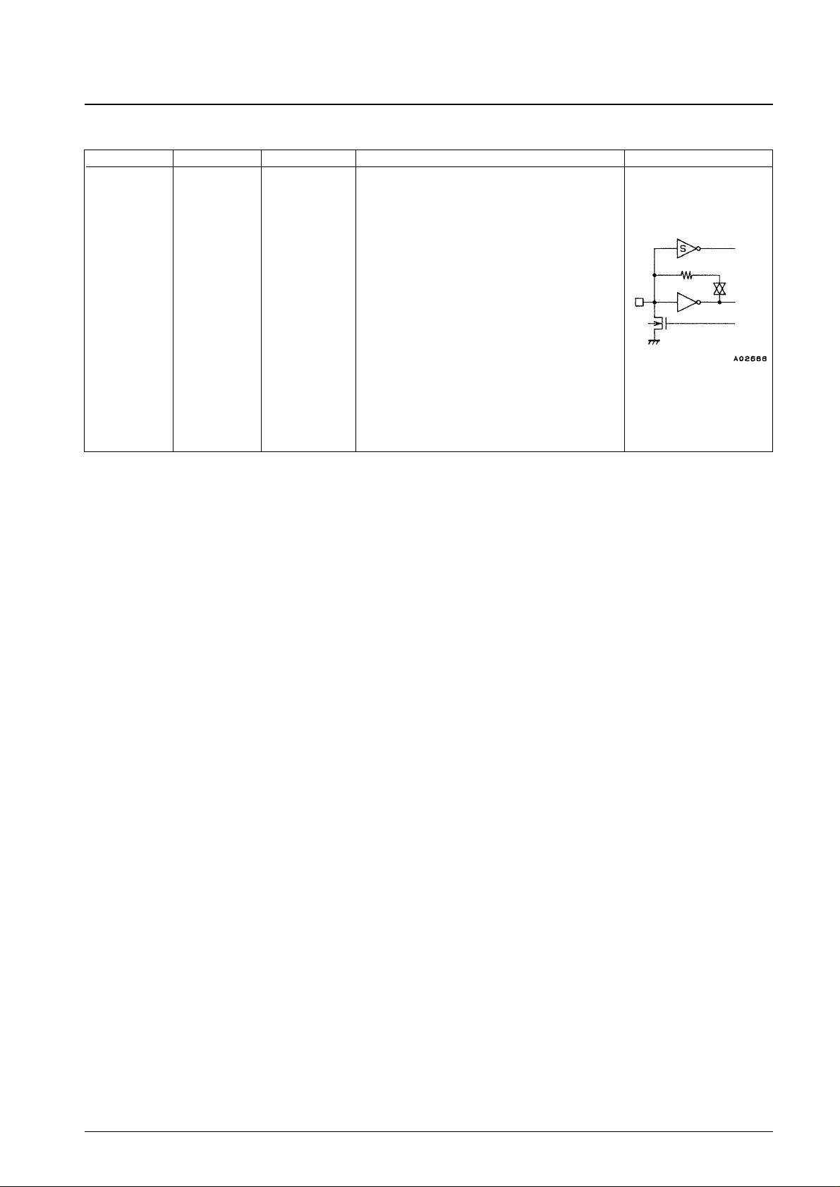
Pin Functions
No. 4922-5/21
LC72146, 72146M
Number Symbol Type Function Equivalent circuit
24
1
17
16
2
4
18
23
XIN
XOUT
Xtal OSC
FMIN
Local oscillator
signal input
AMIN
Local oscillator
signal input
CE
Chip enable
CL Clock
DI
Input data
DO Output data
V
DD
Power supply
V
DD
Ground
Connection for crystal oscillator element (7.2 or 4.5 MHz)
• Serial data input: FMIN is selected when DVS is set to 1.
Input frequency range: 10 to 160 MHz
• The signal is transmitted directly to the swallow counter
• Divisor value range: 272 to 65535
• Serial data input: AMIN is selected when DVS is set to 0.
• Serial data input: when SNS is set to 1.
• Input frequency range: 2 to 40 MHz
• The signal is transmitted directly to the swallow counter.
• Divisor value range: 272 to 65535
• Serial data input: when SNS is set to 0.
• Input frequency range: 0.5 to 10 MHz
• The signal is transmitted directly to the 12-bit
programmable divider.
• Divisor value range: 4 to 4095
12
11
10
I/O-1
I/O-2
I/O-3
General-purpose
I/O port
• General-purpose I/O ports
• Output mode circuit type: open drain
• Function after a power on reset: input port
• Can be set up to function as output ports by bits I/O-1 to
I/O-3 in the serial data sent from the controller.
• IThis pin must be set high to input serial data to the
LC72146 DI pin or to output serial data from the DO pin.
• Inputs the clock used for data synchronization when
inputting serial data to the LC72146 DI pin or outputting
serial data from the DO pin.
• Input pin for serial data transmitted to the LC72146 from
a controller.
• Output pin for serial data transmitted from the LC72146 to
a controller.
• The LC72146 power supply connection. A voltage
between 4.5 and 5.5 volts must be supplied when the
PLL circuit is used.
• The power on reset circuit operates when power is first
applied.
Continued on next page.
• The LC72146 ground connection.
3
15
5
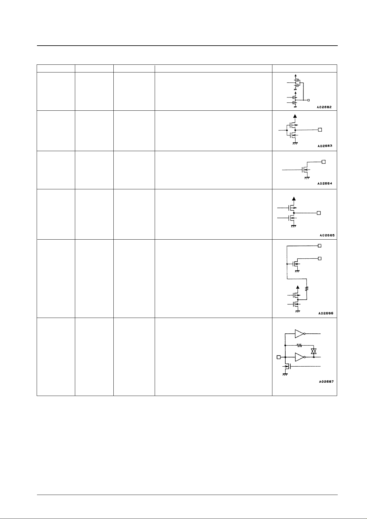
Continued from preceding page.
Number Symbol Type Function Equivalent circuit
No. 4922-6/21
LC72146, 72146M
7 O-6
Output port
• The LC72146 latches the OUT6 bit in the serial data and
outputs it from pin O-6.
6 O-7
Output port
• The LC72146 latches the OUT7 bit in the serial data and
outputs it from pin O-7.
• Outputs a time base signal (8 Hz) when TBC is set to 1.
• Function after a power on reset: open circuit
9
8
I/O-4
I/O-5
General-purpose
I/O port
• General-purpose I/O ports
• Output mode circuit type: complementary
• Function after a power on reset: input port
• Can be set up to function as output ports by bits I/O-4
and I/O-5 in the serial data sent from the controller.
20
19
PD0
PD1
Charge pump
output
• PLL charge pump output pin
If the frequency generated by dividing the local oscillator
frequency by N is higher than the reference frequency, a
high level will be output from PD0, and if it is lower, a low
level will be output. PD0 goes to the high-impedance
state when the frequencies match.
• PD1 operates identically.
21
22
AIN
AOUT
Connections for the
low-pass filter
transistor
• Connections to the n-channel MOS transistor used for
the PLL active low-pass filter.
• A high-speed locking circuit can be formed by using
these pins with the built-in sub charge pump.
• See the item on the structure of the charge pump for
details.
Continued on next page.
14 HCTR/I-6
General-purpose
counter
• HCTR is selected when CTS1 is set to 1.
• Input frequency range: 0.4 to 25 MHz
• The signal is passed through a divide-by-two circuit and
then input to a general-purpose counter. This input also
supports an integrating count function.
• The result is output from the DO output pin starting with
the MSB of the general-purpose counter.
• See the item on the structure of the general-purpose
counter for details.
• When the H/I-6 bit in the serial data is set to 0:
• This pin functions as an input port, and the value input is
output from the DO pin.
No. 4922-7/21
LC72146, 72146M
Continued from preceding page.
Number Symbol Type Function Equivalent circuit
13 LCTR/I-7
General-purpose
counter
• LCTR is selected when CTS1 is set to 0.
• If the CTS0 bit in the serial data is set to 1:
• The circuit operates in frequency measurement mode.
• nput frequency range: 10 to 500 kHz
• The signal is directly transmitted to the general-purpose
counter without passing through the divide-by-two circuit.
• If the CTS0 bit in the serial data is set to 0:
• The circuit operates in period measurement mode.
• nput frequency range: 1 Hz to 20 kHz
• The measurement period can be set to be either one or
two periods of the input signal, and if two period
measurement is selected, the input frequency range
becomes 2 Hz to 40 kHz.
• The result is output from the DO output pin starting with
the MSB of the general-purpose counter.
• See the item on the structure of the general-purpose
counter for details.
• When the L/I-7 bit in the serial data is set to 0:
• This pin functions as an input port. The value input is
output from the DO pin.
 Loading...