

SANYO LC72144M Datasheet
Ordering number : EN5377B
82097HA (OT)/N3096HA (OT)/73096HA (OT) No. 5377-1/22
LC72144M
SANYO Electric Co.,Ltd. Semiconductor Bussiness Headquarters
TOKYO OFFICE Tokyo Bldg., 1-10, 1 Chome, Ueno, Taito-ku, TOKYO, 110 JAPAN
PLL Frequency Synthesizer
CMOS LSI
Overview
The LC72144M is an electronic tuning PLL frequency
synthesizer for use in car and home products, and allows
high-performance multifunction tuners to be implemented
easily, since it includes an A/D converter, a high-speed
lockup circuit, and a crystal oscillator circuit that support
AM up-conversion.
Features
• High-speed programmable dividers for
— 10 to 160 MHz on FMIN using pulse swallower
— 0.5 to 40.0 MHz on AMIN using pulse swallower
and direct division
• General-purpose counters
— HCTR for 0.4 to 25.0 MHz frequency measurement
— LCTR for 10 to 500 kHz frequency measurement
and 4.0 Hz to 20 × 103 Hz period measurement
• 4.5, 7.2, 10.25 or 10.35 MHz crystal
• Twelve selectable reference frequencies (1, 3*2, 5, 9*2,
10, 3.125, 6.25, 12.5, 25, 30*2, 50 and 100*1kHz)
Note: 1. Not supported when a 10.35 or 10.25 MHz
crystal oscillator is used.
2. Not supported when a 10.25 MHz crystal
oscillator is used.
• Phase comparator
— Insensitive band control
— Unlock detection
— Sub-charge pump for high-speed locking
— Deadlock clear circuit
• A/D converter: 6 bits, 2 inputs
• Serial data input and output
Supports control and communication in the CCB format
• Power-on reset circuit
• On-chip crystal oscillator output buffer
• Inputs/outputs (using six general-purpose input/output
ports)
• Operating ranges
— Power-supply voltage: 4.5 to 5.5 V
— Operating temperature: –40 to 85°C
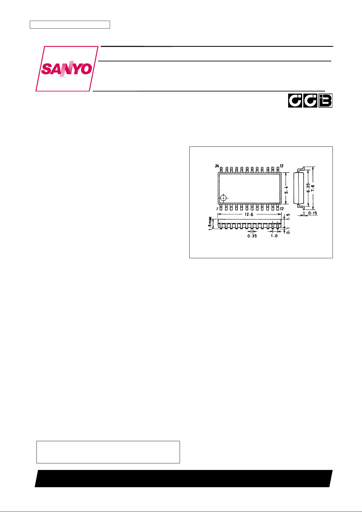
• Package: MFP24S
Package Dimensions
unit: mm
3112-MFP24S
SANYO: MFP24S
[LC72144M]
• CCB is a trademark of SANYO ELECTRIC CO., LTD.
• CCB is SANYO’s original bus format and all the bus
addresses are controlled by SANYO.
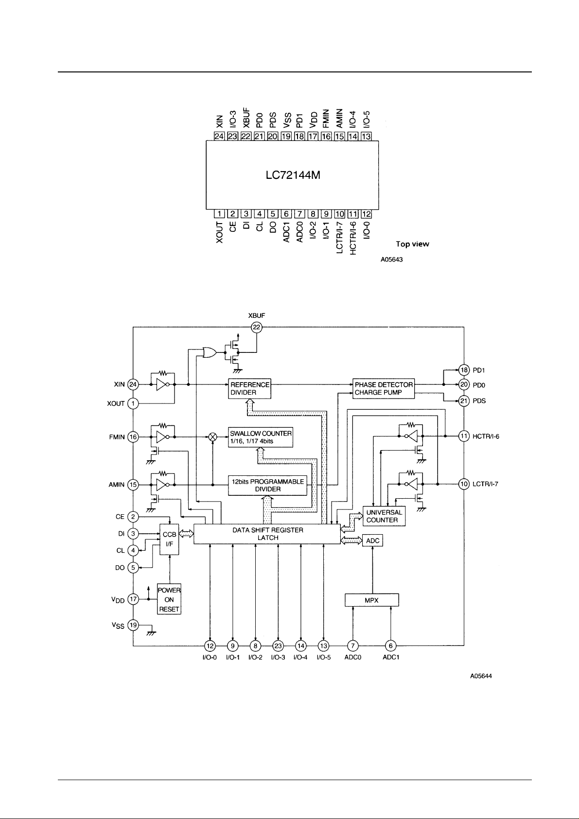
Pin Assignment
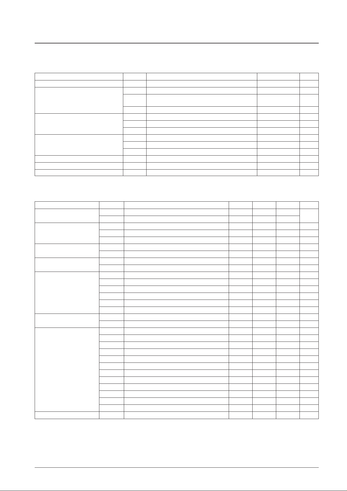
Block Diagram
No. 5377-2/22
LC72144M
Specifications
Absolute Maximum Ratings at Ta = 25°C, VSS= 0 V
Note: A capacitor of at least 2000 pF must be inserted between the power supply, VDD, and VSS.
Allowable Operating Ranges at Ta = –40 to 85°C, VSS= 0 V
Note: 1. Period measurement
2. Refer to the item on the structure of the programmable divider.
3. Serial data: CTC = 0
4. Serial data: CTC = 1
No. 5377-3/22
LC72144M
Parameter Symbol Conditions Ratings Unit
Supply voltage V
DD
max V
DD
–0.3 to +7.0 V
V
IN
1 max CE, CL, DI –0.3 to +7.0 V
Maximum input voltage V
IN
2 max
XIN, FMIN, AMIN, HCTR/I-6, LCTR/I-7, I/O-0, I/O-4, I/O-5,
–0.3 to VDD+ 0.3 V
ADC0, ADC1
V
IN
3 max I/O-1 to I/O-3 –0.3 to +15 V
V
O
1 max DO –0.3 to +7.0 V
Maximum output voltage V
O
2 max XOUT, I/O-0, I/O-4, I/O-5, PD0, PD1, PDS, XBUF –0.3 to VDD+ 0.3 V
V
O
3 max I/O-1 to I/O-3 –0.3 to +15 V
I
O
1 max I/O-0, I/O-4, I/O-5, XBUF 0 to 3.0 mA
Maximum output current I
O
2 max DO 0 to 6.0 mA
I
O
3 max I/O-1 to I/O-3 0 to 10 mA
Allowable power dissipation Pd max Ta ≤85°C 220 mW
Operating temperature Topr –40 to +85 °C
Storage temperature Tstg –55 to +125 °C
Parameter Symbol Conditions min typ max Unit
Supply voltage
V
DD
1 V
DD
4.5 5.5
V
V
DD
2 VDD: Serial data hold voltage 2.0
V
IH
1 CE, CL, DI, I/O-1 to I/O-3 2.2 6.5 V
Input high-level voltage V
IH
2 I/O-0, I/O-4, I/O-5, HCTR/I-6, LCTR/I-7 2.2 V
DD
V
V
IH
3 LCTR/I-7: Pulse waveform, *1 2.2 V
DD
V
Input low-level voltage
V
IL
1 CE, CL, DI, I/O-0 to I/O-5, HCTR/I-6, LCTR/I-7 0 0.8 V
V
IL
2 LCTR/I-7: Pulse waveform, *1 0 0.8 V
Output voltage
V
O
1 DO 0 6.5 V
V
O
2 I/O-1 to I/O-3 0 13 V
f
IN
1 XIN: Sine wave, capacitor coupled 1.0 8.0 MHz
f
IN
2 FMIN: Sine wave, capacitor coupled 10 160 MHz
Input frequency
f
IN
3 AMIN: Sine wave, capacitor coupled 0.5 40 MHz
f
IN
4 HCTR/I-6: Sine wave, capacitor coupled 0.4 25 MHz
f
IN
5 LCTR/I-7: Sine wave, capacitor coupled 10 500 kHz
f
IN
6 LCTR/I-7: Pulse waveform, DC coupled, *1 4.0 20 × 10
3
Hz
Guaranteed crystal
Xtal1 XIN, XOUT: CI ≤ 120 Ω 4.0 7.0 MHz
oscillator ranges
Xtal2 XIN, XOUT: CI ≤ 50 Ω 7.1 10.5 MHz
V
IN
1 XIN 200 1500 mVrms
V
IN
2-1 FMIN: 10 ≤ f < 130 MHz, *2 40 1500 mVrms
V
IN
2-2 FMIN: 130 ≤ f < 160 MHz, *2 70 1500 mVrms
V
IN
3-1 AMIN: 2 ≤ f < 25 MHz, *2 40 1500 mVrms
V
IN
3-2 AMIN: 25 ≤ f < 40 MHz, *2 70 1500 mVrms
Input amplitudes
V
IN
3-3 AMIN: 0.5 ≤ f < 2.5 MHz, *2 40 1500 mVrms
V
IN
3-4 AMIN: 2.5 ≤ f ≤ 10 MHz, *2 70 1500 mVrms
V
IN
4-1 HCTR/I-6: 0.4 ≤ f ≤ 25 MHz, *3 40 1500 mVrms
V
IN
4-2 HCTR/I-6: 8 ≤ f ≤ 12 MHz, *4 70 1500 mVrms
V
IN
5-1 LCTR/I-7: 10 ≤ f < 400 kHz, *3 40 1500 mVrms
V
IN
5-2 LCTR/I-7: 400 ≤ f < 500 kHz, *3 20 1500 mVrms
V
IN
5-3 LCTR/I-7: 400 ≤ f < 500 kHz, *4 70 1500 mVrms
Input voltage range V
IN
6 ADC0, ADC1 0 V
DD
V
Continued on next page.
Continued from preceding page.
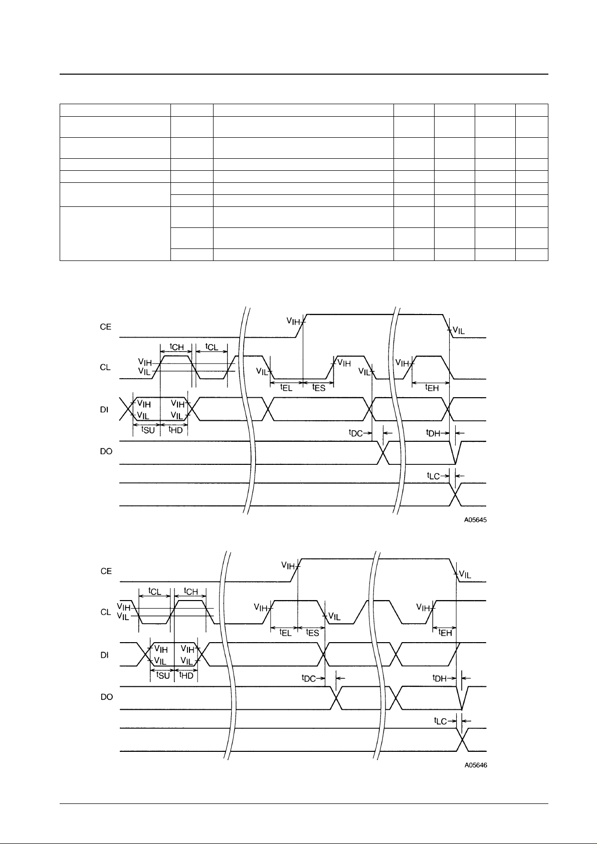
Note: Refer to the serial data timing.
Electrical Characteristics for the Allowable Operating Ranges
No. 5377-4/22
LC72144M
Parameter Symbol Conditions min typ max Unit
Data setup time t
SU
DI, CL: *1 0.45 µs
Data hold time t
HD
DI, CL: *1 0.45 µs
Clock low-level time t
CL
CL: *1 0.45 µs
Clock high-level time t
CH
CL: *1 0.45 µs
CE wait time t
EL
CE, CL: *1 0.45 µs
CE setup time t
ES
CE, CL: *1 0.45 µs
CE hold time t
EH
CE, CL: *1 0.45 µs
Data latch change time t
LC
*1 0.45 µs
t
DC
DO, CL
Differs depending on the values of
0.2 µs
Data output time the pull-up resistor and the printed circuit
t
DH
DO, CE
board capacitances. *1
0.2 µs
Parameter Symbol Conditions min typ max Unit
R
f
1 XIN 1.0 MΩ
R
f
2 FMIN 500 kΩ
Built-in feedback resistors R
f
3 AMIN 500 kΩ
R
f
4 HCTR/I-6 250 kΩ
R
f
5 LCTR/I-7 250 kΩ
Hysteresis V
HIS
CE, CL, DI, LCTR/I-7 0.1 V
DD
V
I
O
= –0.5 mA VDD– 0.5 V
High-level output voltage
V
OH
1 PD0, PD1, PDS, I/O-0, I/O-4, I/O-5 IO= –1 mA VDD– 1.0 V
I
O
= –2 mA VDD– 2.0 V
V
OH
2 XBUF IO= –0.5 mA VDD– 1.5 V
I
O
= 0.5 mA 0.5 V
V
OL
1 PD0, PD1, PDS, I/O-0, I/O-4, I/O-5 IO= 1 mA 1.0 V
I
O
= 2 mA 2.0 V
V
OL
2 XBUF IO= 0.5 mA 1.5 V
Low-level output voltage I
O
= 1 mA 0.2 V
V
OL
3 I/O-1 to I/O-3
I
O
= 2.5 mA 0.5 V
I
O
= 5 mA 1.0 V
I
O
= 9 mA 1.8 V
V
OL
4 DO: IO= 5 mA 1.0 V
I
IH
1 CE, CL, DI: VI= 6.5 V 5.0 µA
I
IH
2 I/O-1 to I/O-3: VI= 13 V 5.0 µA
I
IH
3
I/O-0, I/O-4, I/O-5, ADC0, ADC1, HCTR/I-6, LCTR/I-7:
5.0 µA
High-level input current V
I
= V
DD
IIH4 XIN: VI= V
DD
2.0 11 µA
I
IH
5 FMIN, AMIN: VI= V
DD
4.0 22 µA
I
IH
6 HCTR/I-6, LCTR/I-7: VI= V
DD
8.0 44 µA
I
IL
1 CE, CL, DI: VI= 0 V 5.0 µA
I
IL
2 I/O-0, to I/O-3: VI= 0 V 5.0 µA
I
IL
3
I/O-0, I/O-4, I/O-5, ADC0, ADC1, HCTR/I-6, LCTR/I-7:
5.0 µA
Low-level input current V
I
= 0 V
I
IL
4 XIN: VI= 0 V 2.0 11 µA
I
IL
5 FMIN, AMIN: VI= 0 V 4.0 22 µA
I
IL
6 HCTR/I-6, LCTR/I-7: VI= 0 V 8.0 44 µA
Output off leakage current
I
OFF
1 I/O-1 to I/O-3: VO= 13 V 5.0 µA
I
OFF
2 DO: VO= 6.5 V 5.0 µA
Continued on next page.
Continued from preceding page.
Serial Data Timing
When CL is stopped at the low level
When CL is stopped at the high level
No. 5377-5/22
LC72144M
Parameter Symbol Conditions min typ max Unit
High-level 3-state off
I
OFFH
PD0, PD1, PDS: VO= V
DD
0.01 200 nA
leakage current
Low-level 3-state off
I
OFFL
PD0, PD1, PDS: VO= 0 V 0.01 200 nA
leakage current
Input capacitance C
IN
FMIN 6 pF
A/D converter linearity error Err ADC0, ADC1 –0.5 +0.5 LSB
Pull-down transistor on resistance
Rpd1 FMIN 80 200 600 kΩ
Rpd2 AMIN 80 200 600 kΩ
I
DD
1
V
DD
: Xtal = 10.35 MHz, fIN2 = 160 MHz,
10 15 mA
V
IN
2 = 70 mVrms, fIN4 = 25 MHz, VIN4 = 40 mVrms
Current drain
I
DD
2
V
DD
: PLL block stopped (PLL INHIBIT),
0.5 1.5 mA
Xtal oscillator operating (Xtal = 10.35 MHz)
I
DD
3 VDD: PLL block stopped, Xtal oscillator stopped 10 µA
Internal
data
latching
Old
Internal
data
latching
Old
New
New
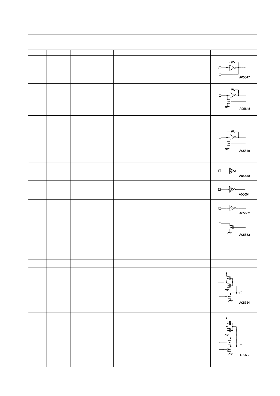
Pin Functions
No. 5377-6/22
LC72144M
Pin No. Symbol Type Function Pin circuit
24
1
16
15
2
4
3
5
17
19
9
8
23
12
14
13
XIN
XOUT
FMIN
AMIN
CE
CL
DI
DO
V
DD
V
SS
I/O-1
I/O-2
I/O-3
I/O-0
I/O-4
I/O-5
Xtal oscillator
Local oscillator
signal input
Local oscillator
signal input
Chip enable
Clock
Input data
Output data
Power supply
Ground
General-purpose
I/O ports
General-purpose
I/O ports
Crystal oscillator connection
(4.5, 7.2, 10.25, or 10.35 MHz)
FMIN is selected when DVS in the serial data input is set to 1.
The input frequency range is 10 to 160 MHz.
The signal is transmitted to the swallow counter.
The divisor can be set to a value in the range 272 to 65,535.
AMIN is selected when DVS in the serial data input is set to 0.
When SNS in the serial data input is set to 1:
• The input frequency range is 2 to 40 MHz.
• The signal is transmitted to the swallow counter.
• The divisor can be set to a value in the range 272 to 65,535.
When SNS in the serial data input is set to 0:
• The input frequency range is 0.5 to 10 MHz.
• The signal is transmitted to the 12-bit programmable divider.
• The divisor can be set to a value in the range 4 to 4,095.
This pin must be set high during serial data input (DI) to the
LC72144M, or during serial data output (DO).
Used for data synchronization during serial data input (DI) to
the LC72144M, or during serial data output (DO).
Used to input serial data transferred to the LC72144M from the
controller.
Used to output serial data transferred the controller from the
LC72144M.
The LC72144M power supply connection. Provide a voltage
between 4.5 and 5.5 V when the PLL circuit is in operation.
The power on reset circuit operates when power is first applied.
—
The LC72144M ground connection. —
General-purpose I/O ports
The output circuits are open-drain circuits.
I/O-1 and I/O-2 are set to be input ports after the power on
reset. I/O-3 becomes an output port fixed at the low level.
These pins are switched between input and output by the I/O-1
to I/O-3 bits in the serial data transferred from the controller.
General-purpose I/O ports
The output circuits are complementary circuits.
These ports are set to be input ports after the power on reset.
These pins are switched between input and output by the I/O-0,
I/O-4, and I/O-5 bits in the serial data transferred from the
controller.
Continued on next page.
Continued from preceding page.
No. 5377-7/22
LC72144M
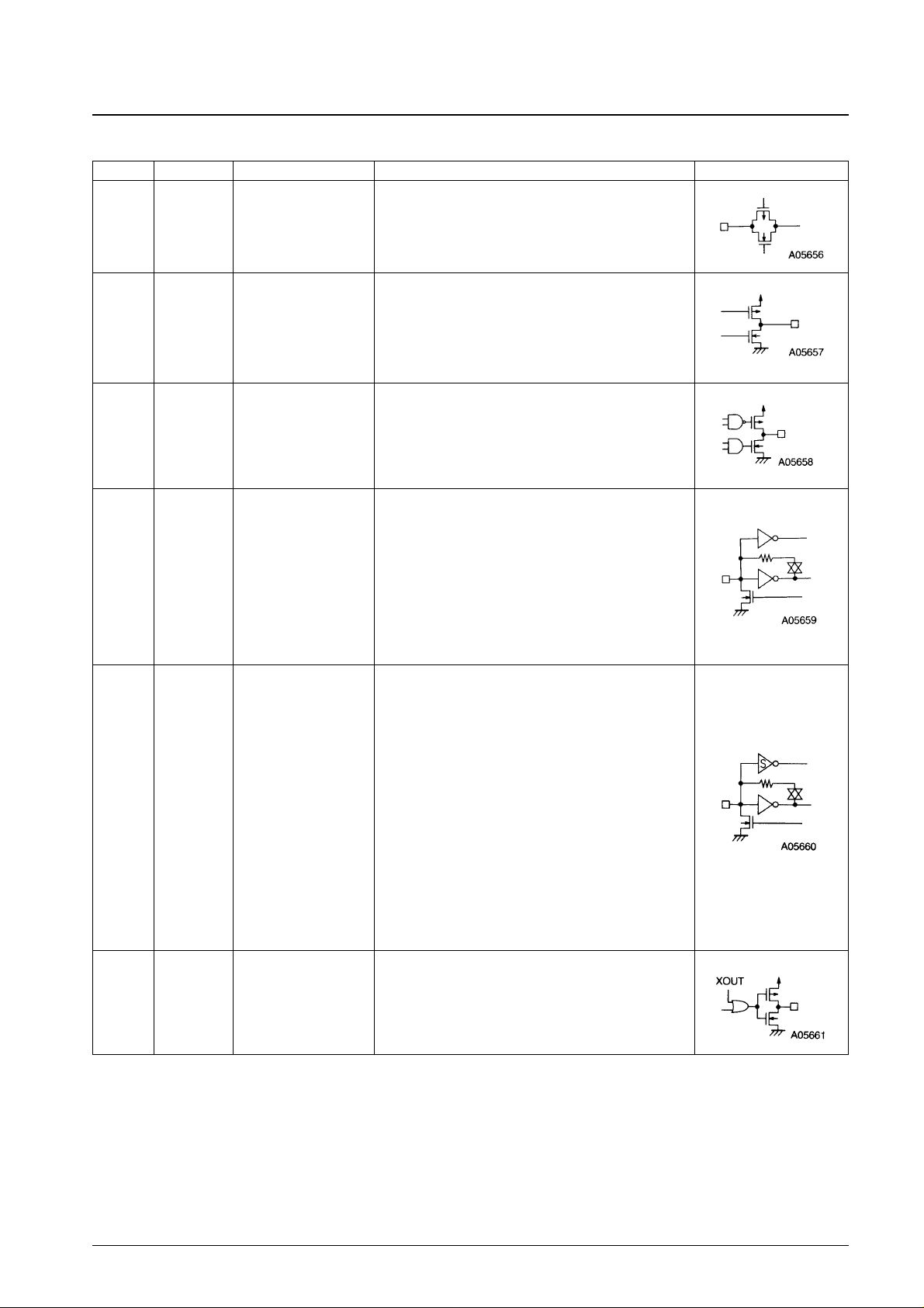
Pin No. Symbol Type Function Pin circuit
7
6
21
18
20
11
10
22
ADC0
ADC1
PD0
PD1
PDS
HCTR/I-6
LCTR/I-7
XBUF
A/D converter input
Main charge pump output
Sub-charge pump output
General-purpose counter
General-purpose counter
Xtal oscillator buffer
A/D converter inputs
6-bit successive-approximation A/D converter
See the item on the structure of the A/D converter for details.
PLL charge pump output
A high level is output from the PD0 pin when the frequency
created by dividing the local oscillator frequency by N is higher
than the reference frequency. A low level is output when the
frequency is lower. The pin goes to the high-impedance state
when the frequencies agree.
The PD1 pin operates in the same manner.
A high-speed lockup circuit can be formed by using this pin in
combination with the main charge pump.
See the item on the structure of the charge pump for details.
HCTR is selected when the CTS1 bit in the serial data is set to 1.
• The input frequency range is 0.4 to 25 MHz.
• The signal passes through a divide-by-2 circuit and then is
input to a general-purpose counter. An integrating count can
also be performed.
• The result of the count is output from the MSB of the generalpurpose counter through the DO output pin.
• See the item on the structure of the general-purpose counter
for details.
When the serial data H/I-6 bit is set to 0:
• This pin functions as an input port, and its state is output from
the DO output pin.
LCTR is selected when the CTS1 bit in the serial data is set to 0.
When the CTS0 bit in the serial data is set to 1:
• The circuit switches to frequency measurement mode.
• The input frequency range is 10 to 500 kHz.
• The signal is input directly to the general-purpose counter
without passing through the divide-by-2 counter.
• The result of the count is output from the MSB of the generalpurpose counter through the DO output pin.
When the CTS0 bit in the serial data is set to 0:
• The circuit switches to period measurement mode.
• The input frequency range is 4 Hz to 20 kHz.
• The measurement period can be set to be 1 or 2 periods.
• The result of the count is output from the MSB of the generalpurpose counter through the DO output pin.
• See the item on the structure of the general-purpose counter
for details.
When the L/I-7 bit in the serial data is set to 0.
• This pin functions as an input port, and its state is output from
the DO output pin.
Output buffer for the crystal oscillator circuit.
If the XB bit in the serial data is set to 1, the output buffer
operates and the crystal oscillator signal (a pulse waveform) is
output.
If XB is 0, this pin outputs a low level. (Since XB is set to 0 after
the power on reset, the output will be fixed at the low level.)
 Loading...