


Any and all SANYO products described or contained herein do not have specifications that can handle
applications that require extremely high levels of reliability, such as life-support systems, aircraft’s
control systems, or other applications whose failure can be reasonably expected to result in serious
physical and/or material damage. Consult with your SANYO representative nearest you before using
any SANYO products described or contained herein in such applications.
SANYO assumes no responsibility for equipment failures that result from using products at values that
exceed, even momentarily, rated values (such as maximum ratings, operating condition ranges, or other
parameters) listed in products specifications of any and all SANYO products described or contained
herein.
Overview
The LC5822, LC5823, and LC5824 are CMOS
microcontrollers that feature the low-voltage operation
required for battery-power applications and that provide
4 KB, 6 KB, or 8 KB of ROM, 1 kilobit of RAM, and an
LCD driver.
These microcontrollers support an instruction set based on
that of the earlier LC5800, LC5812, and LC5814 for
excellent efficiency in software development.
Applications
• LCD display in multi-function watches, timers, and
other products
• Control and LCD display in timers
• Control and LCD display in miniature test equipment,
health maintenance equipment, and other products
• These microcontrollers are optimal for products that
include an LCD display, especially battery powered
products.
Wide Allowable Operating Ranges
Note*: When the backup flag is set, the BAK pin is connected to VDD.
Features
• These microcontrollers are high-end versions of the
LC5800 and provide the following features.
Low Current Drain * In halt mode (typical)
• Ceramic oscillator 400 kHz (3.0 V) 200 µA
• Crystal oscillator 32 kHz (1.5 V, Ag specifications)
3.0 µA (LCD biases other than 1/3) 4.5 µA (LCD drive:
1/3 bias)
• Crystal oscillator 32 kHz (3.0 V, Li specifications)
2.0 µA (LCD biases other than 1/3) 6.0 µA (LCD drive:
1/3 bias)
Timer and Counter Functions
• One 8-bit programmable timer (May be used as an event
counter)
• One 8-bit programmable reload timer
• Time base timer (for clocks)
• Watchdog timer
• 8-bit serial I/O (3-pin synchronous system)
Standby Functions
• Clock standby function (halt mode)
Only the oscillator circuits, the divider circuit, and the
LCD driver operate. All other internal operations are
stopped. This provides a power-saving function in which
current drain is minimized, and allows a clock function
to be implemented easily with low power dissipation.
Furthermore, low-speed and high-speed modes can be
implemented by setting the operating modes of the two
oscillator circuits.
• Full standby function (hold mode)
• Halt mode can be cleared by any of two external and
two internal interrupts.
CMOS IC
82198RM (OT) No. 5944-1/24
SANYO Electric Co.,Ltd. Semiconductor Bussiness Headquarters
TOKYO OFFICE Tokyo Bldg., 1-10, 1 Chome, Ueno, Taito-ku, TOKYO, 110-8534 JAPAN
4-Bit Single-Chip Microcontrollers Featuring 4 KB to 8 KB of ROM, 1 Kbit of RAM,
and an LCD Driver for Medium Speed Small-Scale Control Applications
LC5824, LC5823, LC5822
Ordering number : EN5944
Power Cycle Supply
options times voltage Notes
supply range
EXT-V 10 µs V
DD
= 2.3 to 3.6 V
When an 800-kHz ceramic
oscillator is used
EXT-V 20 µs V
DD
= 2.3 to 3.6 V
When an 400-kHz ceramic
oscillator is used
EXT-V 61 µs V
DD
= 2.3 to 3.6 V
When an 65-kHz crystal oscillator
is used
EXT-V 122 µs V
DD
= 2.0 to 3.6 V
When an 32-kHz crystal oscillator
is used
Li 122 µs V
DD
= 2.6 to 3.6 V*
When an 32-kHz crystal oscillator
is used
Ag 122 µs V
DD
= 1.3 to 1.65 V
When an 32-kHz crystal oscillator
is used
Improved I/O Functions
• External interrupt pins
• Input pins that can clear halt mode:
10 pins (maximum)
• Input ports with input resistors that can be controlled
from software: 8 pins (maximum)
• Pins with a function that prevents the input port floating
state: 8 pins (maximum)
• LCD drive pins: 4 pins (common), 42 pins (segment outputs)
• General-purpose I/O ports:
16 pins (when all 4 P port pins are used)
• General-purpose inputs: 8 pins
• General-purpose outputs (1):1 pin (the ALM pin)
• General-purpose outputs (2):
42 pins (when all 42 of the
LCD segment outputs are
switched over to function as
general-purpose outputs)
• 8-bit serial output port: 1 set (3 pins: output, input,
and clock)
Functional Overview
• Program ROM: 4096 × 16 bits LC5824
3072 × 16 bits LC5823
2048 × 16 bits LC5822
• Internal RAM: 256 × 4 bits
• All instructions execute in a single cycle.
• Extensive set of interrupt functions for clearing halt and
hold mode
— 8 halt mode clearing functions
— 5 hold mode clearing functions
— 6 interrupt functions
— Subroutines can be nested up to 8 levels (Special-
purpose registers that are shared with the interrupt
function are built in.)
• Powerful hardware to increase system processing capacity
— Segment port related hardware
Built-in segment PLA circuit
Built-in segment decoder
Support for six different LCD drive specifications
Outputs can be switched to CMOS levels
— Built-in 8-bit synchronous serial I/O circuit
— 8-bit read/write timer (plus a separate 8-bit
prescaler; can be used as and event counter)
— 8-bit reload timer (plus built-in 8-bit prescaler)
— Built-in 8-bit prescaler (for use with timer 1, timer 2,
and the serial counter)
— All of RAM can be used a working area (RAM bank
system)
— Dedicated data pointer register for RAM access
— 15-stage divider circuit for clocks (also used as the
LCD voltage alternation frequency generator)
— 8-bit table reference function (reads 8-bit ROM data)
— Chattering prevention circuit (on two ports)
— Alarm signal generation circuit
• LCD panel drive output pins with high flexibility
(42 pins)
— The LCD output pins can be switched to function as
general-purpose outputs.
CMOS/p-channel/n-channel type combinations: Up
to 42 pins
— An alternation frequency appropriate for the LCD
panel used can be selected.
• An oscillator appropriate for your system’s specifications
can be selected.
— A 32- or 65-kHz crystal oscillator can be selected
(Used when a clock function is required or for low
current drain operation.)
— A ceramic oscillator with a frequency from 400 kHz
to 2 MHz can be selected (when high-speed
operation is required.)
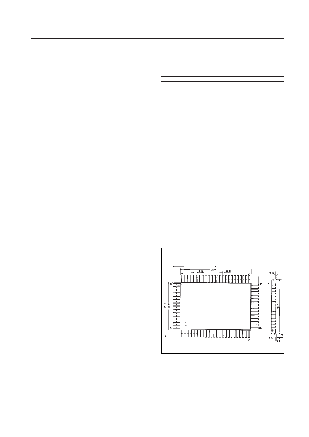
Available delivery formats: QIP-80 and chip
Package Dimensions
unit: mm
3174-QFP80E
No. 5944-2/24
LC5824, LC5823, LC5822
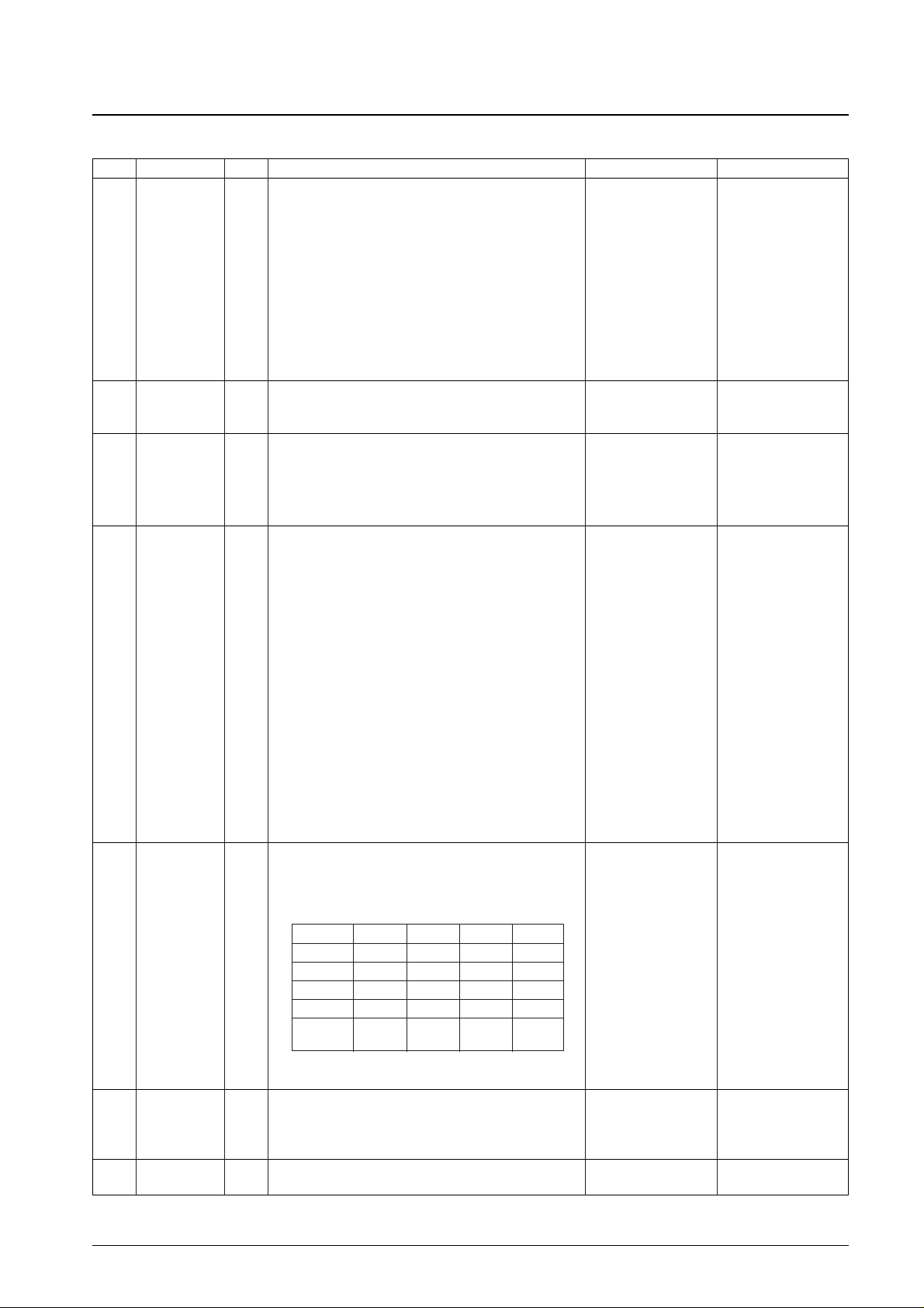
Drive system Number of driven segments
Required number of common pins
bias · duty 168 segments 4 pins
bias · duty 126 segments 3 pins
bias · duty 168 segments 4 pins
bias · duty 126 segments 3 pins
bias · duty 84 segments 2 pins
Static drive 42 segments 1 pin
[LC5824, 5823, 5822]
SANYO: QIP80E
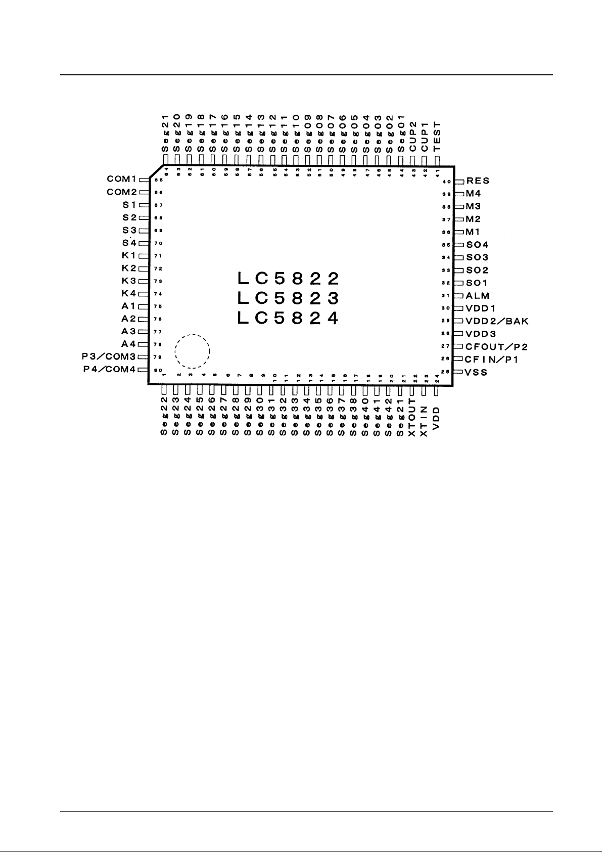
Pin Assignment
No. 5944-3/24
LC5824, LC5823, LC5822
Top view
No. 5944-4/24
LC5824, LC5823, LC5822
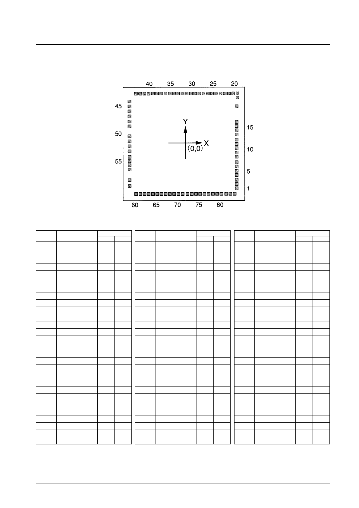
Pad Arrangement
Chip size: 4.92 mm × 5.15 mm
Pad size: 120 µm × 120 µm
Chip thickness 480 µm (chip specifications)
Pad Coordinates
PAD No. Pin
Coordinates
X
µmY µm
60 Seg 22 –2030 –2178
61 Seg 23 –1850 –2178
62 Seg 24 –1670 –2178
63 Seg 25 –1490 –2178
64 Seg 26 –1310 –2178
65 Seg 27 –1130 –2178
66 Seg 28 –950 –2178
67 Seg 29 –770 –2178
68 Seg 30 –590 –2178
69 Seg 31 –410 –2178
70 Seg 32 –230 –2178
71 Seg 33 –50 –2178
72 Seg 34 122 –2178
73 Seg 35 302 –2178
74 Seg 36 482 –2178
75 Seg 37 662 –2178
76 Seg 38 842 –2178
77 Seg 39 1022 –2178
78 Seg 40 1202 –2178
79 Seg 41 1382 –2178
80 Seg 42 1562 –2178
81 XC 1774 –2178
82 XTOUT 1954 –2178
83 XTIN 2134 –2178
1 V
DD
2257 –1959
2 V
SS
2257 –1779
3 CFIN/P1 2257 –1599
4 CFOUT/P2 2257 –1402
PAD No. Pin
Coordinates
X
µmY µm
5 VDD3 2257 –1212
6 V
DD
2/BAK 2257 –1032
7 V
DD
1 2257 –852
8 ALM 2257 –601
9 SO1 2257 –419
10 SO2 I/O port 2257 –236
11 SO3 I/O port 2257 56
12 SO4 I/O port 2257 132
13 M1 2257 364
14 M2 I/O port 2257 544
15 M3 I/O port 2257 724
16 M4 I/O port 2257 904
17 RES I/O port 2257 1636
18 Test 2330 1998
19 Test 2330 2178
20 TST 2150 2178
21 CUP1 1970 2178
22 CUP2 1790 2178
23 Seg 1 1606 2178
24 Seg 2 1426 2178
25 Seg 3 1246 2178
26 Seg 4 1066 2178
27 Seg 5 886 2178
28 Seg 6 706 2178
29 Seg 7 526 2178
30 Seg 8 346 2178
31 Seg 9 166 2178
32 Seg 10 –14 2178
PAD No. Pin
Coordinates
X
µmY µm
33 Seg 11 –194 2178
34 Seg 12 –374 2178
35 Seg 13 –546 2178
36 Seg 14 –726 2178
37 Seg 15 –906 2178
38 Seg 16 –1086 2178
39 Seg 17 –1266 2178
40 Seg 18 –1446 2178
41 Seg 19 –1626 2178
42 Seg 20 –1806 2178
43 Seg 21 –1986 2178
44 COM1 –2270 1871
45 COM2 –2270 1628
46 S1 –2270 1367
47 S2 Input port –2270 1140
48 S3 Input port –2270 960
49 S4 Input port –2270 734
50 K1 –2270 328
51 K2 Input port –2270 88
52 K3 Input port –2270 –140
53 K4 Input port –2270 –380
54 A1 –2270 –593
55 A2 I/O ports –2270 –773
56 A3 I/O ports –2270 –953
57 A4 I/O ports –2270 –1133
58 COM3/P3 –2270 –1602
59 COM4/P4 –2270 –1846
Note: • The pin numbers are the QIP-80E mass-production package pin numbers.
• The test pin (TST) must be connected to V
SS
.
• Pads number 42 and 43 in the chip version must be left open.
• Do not use solder dip techniques to mount the QIP-80E package version.
• In the chip version, the substrate must be either connected to V
SS
or left open.
System Block Diagram
No. 5944-5/24
LC5824, LC5823, LC5822
RAM: Data memory
ROM: Program memory
DP: Data pointer register
BNK: Bank register
APG: RAM page flag
AC: Accumulator
ALU: Arithmetic and logic unit
B: B register
OPG: ROM page flag
PC: Program counter
IR: Instruction register
STS1: Status register 1
STS2: Status register 2
STS3: Status register 3
STS4: Status register 4
PLA: Programmed logic array used for segment data and strobe functions
WAIT.C:Wait time counter
Address
Buffer
Accumulator
(AC) (4 bits)
Data I/O - D bus
Timer 1
Timer 2
Carrier control circuit
Interrupt control
Watchdog timer
LCD driver
Reset
circuit
Chronograph
circuit
Chronograph
control circuit
Switch-
ing
circuit
System clock
generator
Voltage step-
Serial I/O
B register
(4 bits)
OPG
(2 bits)
Program
counter
(13 bits)
Clock timer
(15 bits)
Alarm tone
generator
Segment decoder
strobe decoder
Table
reference
Crystal
oscillator
circuit
(32 kHz/65 kHz)
CF/RC oscillator
circuit
(400 kHz to
4 MHz)
No. 5944-6/24
LC5824, LC5823, LC5822
Pin Functions
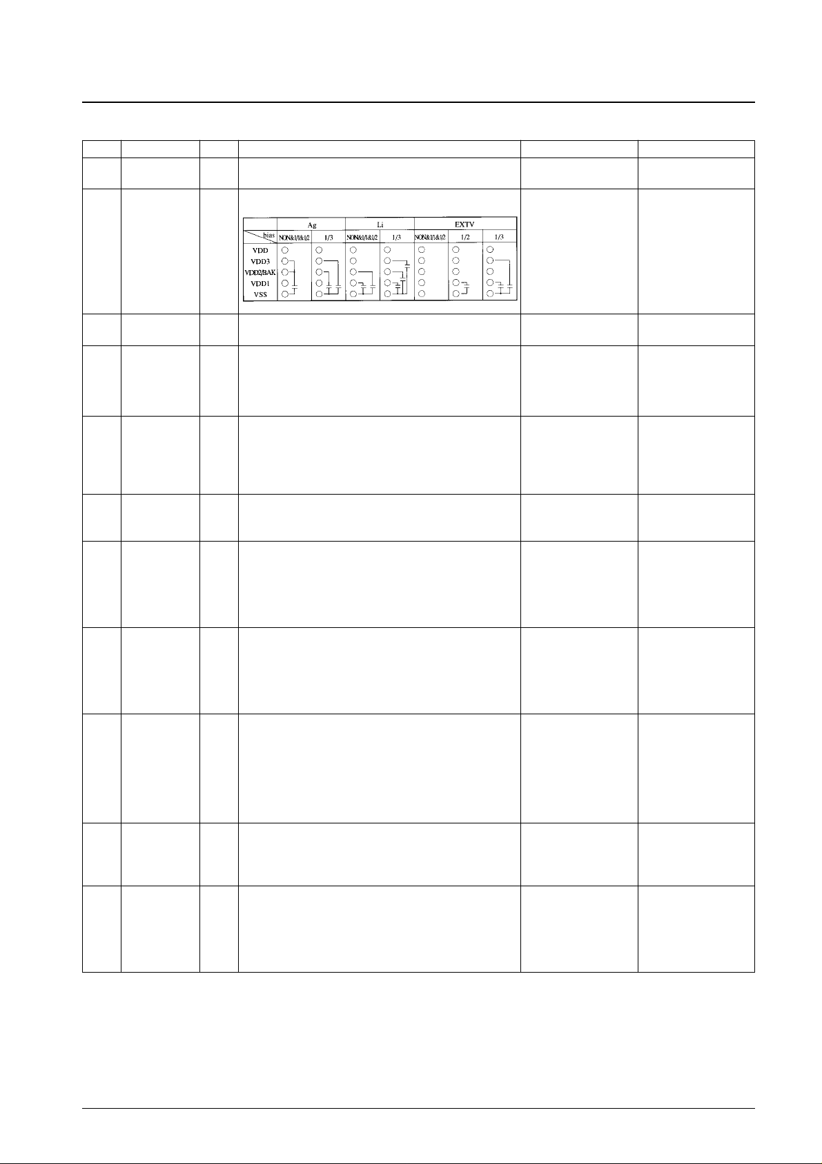
Pin No. Pin I/O Function Options Status at reset
24
25
V
DD
V
SS
—
—
30
29
28
V
DD
1
V
DD
2/BAK
V
DD
3
—
—
—
LCD drive power supply
Power supply
Pin
• Ag specifications
• Li specifications
• EXT-V specifications
42
43
CUP1
CUP2
——Connections of the LCD power supply step-up (step-down)
capacitors
26
27
CFIN
CFOUT
Input
Output
System clock oscillator connections
• Ceramic element connections (CF specifications)
• RC component connections (RC specifications)
*: This oscillator circuit is stopped when a STOP or SLOW
instruction is executed.
• CF specifications
• RC specifications
• Unused
23
22
XTIN
XTOUT
Input
Output
Used for reference counting (clock specifications, LCD
alternation frequency) and as the system clock.
• 32-kHz crystal oscillator
• 65-kHz crystal oscillator
*: This oscillator circuit is stopped when a STOP instruction is
executed.
• 32-kHz specifications
• 65-kHz specifications
• 38-kHz specifications
• Unused
— XC —
Used for the phase compensation capacitor connected between
this pin and XTOUT and XTIN. This pin is only used in the chip
product.
67
68
69
70
S1
S2
S3
S4
Input
Input-only port
• Input pins used to acquire input data to RAM
• 1.95-ms and 7.8-ms chattering exclusion circuits included.
• Pull-down resistors are built in.
Note: the 1.95 ms and 7.8 ms values are for a ø0 of
32.768 kHz.
• Presence or absence of
low-level hold
transistors
• Pull-down resistors
enabled
Note: After a reset is
cleared, these pins go to
the floating state.
71
72
73
74
K1
K2
K3
K4
Input
Input-only port
• Input pins used to acquire input data to RAM
• 1.95-ms and 7.8-ms chattering exclusion circuits included.
• Pull-down resistors are built in.
Note: the 1.95 ms and 7.8 ms values are for a ø0 of
32.768 kHz.
• Presence or absence of
low-level hold
transistors
• Pull-down resistors
enabled
Note: After a reset is
cleared, these pins go to
the floating state.
36
37
38
39
M1
M2
M3
M4
I/O
I/O port
• Input pins used to acquire input data to RAM.
• Output pins used to output RAM data.
• M4 is also used as the TM1 external clock input in TM1 mode 3.
• M3 is also used for HEF8 halt mode clear control.
*: The minimum period for clock signal inputs is twice the cycle
time
• Pull-down resistors are built in.
• Presence or absence of
low-level hold
transistors
• Output type: CMOS or
p-channel
• Pull-down resistors
enabled
Note: After a reset is
cleared, these pins go to
the floating state.
• Input mode
• The output latch data is
set to 1.
26
27
79
80
P1
P2
P3
P4
I/O
I/O port
• Input pins used to acquire input data to RAM.
• Output pins used to output RAM data.
• Pull-down resistors are built in.
The same as those for
M1 to M4. However, only
for valid ports.
The same as those for
M1 to M4. However, only
for valid ports.
76
77
78
79
A1
A2
A3
A4
I/O
I/O port
• Input pins used to acquire input data to RAM.
• Output pins used to output RAM data.
• Pull-down resistors are built in.
• A1 is also used as the external interrupt request control input
signal (INT).
The same as those for
M1 to M4.
The same as those for
M1 to M4.
Continued on next page.
Power supply
specifications
No. 5944-7/24
LC5824, LC5823, LC5822
Continued from preceding page.
Pin No. Pin I/O Function Options Status at reset
32
33
34
35
SO1
SO2
SO3
SO4
I/O
I/O port
• Input pins used to acquire input data to RAM.
• Output pins used to output RAM data.
• Pull-down resistors are built in.
SO1 to SO3 are also used as the serial interface pins.
• The serial interface function can be selected under program
control.
• Pin functions:
SO1: Serial input
SO2: Serial output
SO3: Serial clock
The serial clock can be taken from either internal or external
sources, and can be set up to detect either rising or falling
edges under program control.
Identical to M1 throughM4Identical to M1 through
M4
31 ALM Output
Output-only pin
• A signal modulated by ø0, ø3, or ø4 can be output under
program control.
Low-level output
40 RES Input
IC internal reset input
• The program counter is set to point to location 00H.
• The reset input level can be set to be either high or low.
• Either a pull-up or a pull-down resistor is built in.
Note: Applications must apply the reset signal level for at least
500 µs to effect a reset.
• Selection of a pull-up or
pull-down resistor
• Selection of active-low
or active-high reset
logic
44
64
1
21
Seg 22
Seg 21
Seg 22
Seg 42
Output
LCD panel drive outputs/general-purpose outputs
• LCD panel drive
(1) Static
(2) 1/2 bias 1/2 duty
(3) 1/2 bias 1/3 duty
(4) 1/2 bias 1/4 duty
(5) 1/3 bias 1/3 duty
(6) 1/3 bias 1/4 duty
One of items (1) through (5) is selected as a mask option.
• General-purpose output ports
(1) CMOS output
(2) p-channel open-drain output
(3) n-channel open-drain output
One of items (1) through (3) is selected as a mask option.
• The adoption of the segment PLA in these microcontrollers
means that there is no need for programs to control the
LCD/general-purpose output states of these pins.
• Output latch control is supported in the oscillator stopped
standby states and during a reset.
• Any combination of LCD and general-purpose output functions
may be used.
• Switching between LCD
drive output and
general-purpose output
• Switching between the
LCD drive type options
—Static
—1/2 bias 1/2 duty
—1/2 bias 1/3 duty
—1/2 bias 1/4 duty
—1/3 bias 1/3 duty
—1/3 bias 1/4 duty
• General-purpose output
type switching
—CMOS
—p-channel open-drain
—n-channel open-drain
• Standby mode output
latch control
• When used for LCD
drive:
—All lit
—All off
*Determined by the
master options
• When used as generalpurpose outputs:
—High level
—Low level
*Determined by the
master options
Note: When a
combination of LCD drive
and general-purpose
outputs is selected, these
pins will be either:
All lit/high-level output, or
All off/low-level output.
• During the reset period,
the LCD drive functions
as static drive.
65
66
79
80
COM1
COM2
COM3
COM4
Output
Common drive outputs for the LCD panel
The table below lists which pins are used in each of the drive
types.
However, note that the listed alternation frequencies are the
typical specifications when ø0 is 32.768 kHz.
41 TST Input
Test input
• In the QIP-80 version, this pin must be connected to V
SS
.
• In the chip version, this pin must be left open or connected to
V
SS
.
—
—
TEST
TEST
—
—
Test pins.
(These are not used in the device user interface.)
Note: Note that the “
✕” symbol indicates that the corresponding
common pin cannot be used in that drive type.
*In products with the CF
specifications, the
alternation frequency
signal stops briefly.
Static 1/2 duty 1/3 duty 1/4/duty
COM1
●● ●● ●● ●●
COM2 ✕ ●● ●● ●●
COM3 ✕ ✕ ●● ●●
COM4 ✕ ✕ ✕ ●●
Alternation
32 Hz 32 Hz 42.7 Hz 64 Hz
frequency
No. 5944-8/24
LC5824, LC5823, LC5822
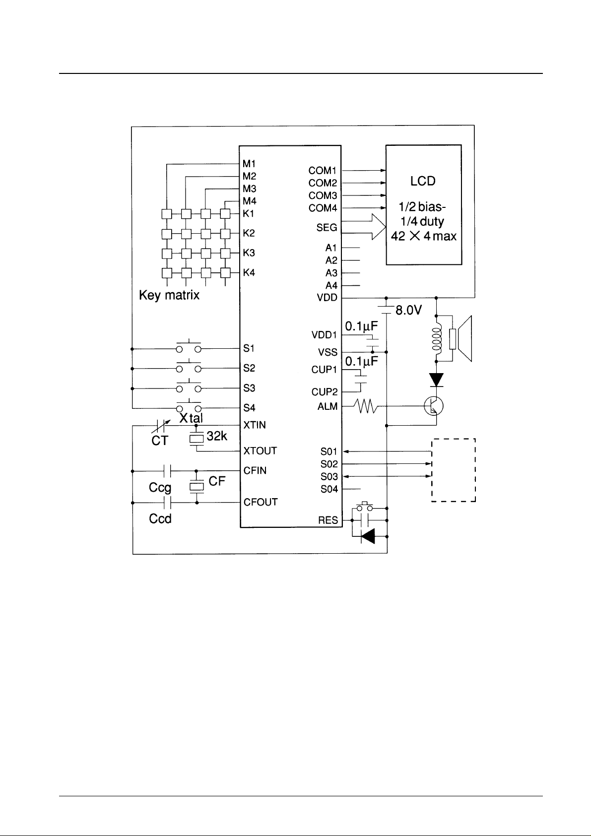
Sample Application Circuit
LCD : 1/2 bias — 1/4 duty
 Loading...