Page 1

Any and all SANYO products described or contained herein do not have specifications that can handle
applications that require extremely high levels of reliability, such as life-support systems, aircraft’s
control systems, or other applications whose failure can be reasonably expected to result in serious
physical and/or material damage. Consult with your SANYO representative nearest you before using
any SANYO products described or contained herein in such applications.
SANYO assumes no responsibility for equipment failures that result from using products at values that
exceed, even momentarily, rated values (such as maximum ratings, operating condition ranges,or other
parameters) listed in products specifications of any and all SANYO products described or contained
herein.
Monolithic Linear IC
VCO Non-Adjusting PLL FM MPX
Stereo Demodulator with FM Accessories
Ordering number:ENN1868C
LA3401
SANYO Electric Co.,Ltd. Semiconductor Company
TOKYO OFFICE Tokyo Bldg., 1-10, 1 Chome, Ueno, Taito-ku, TOKYO, 110-8534 JAPAN
Overview
The LA3401 is a multifunctional MPX demodulator IC
designed for FM stereo electronic tuning. It features the
VCO non-adjusting function that eliminates the need to
adjust free-running frequency of VCO and the accessory
functions such as FM/AM input, FM/AM input changeover ,
muting.
Applications
• Home stereos, portable hi-fi sets.
Functions
• VCO non-adjusting function.
• PLL MPX stereo demodulator.
• Gain variable type post amplifier.
• FM-AM changeover.
• Muting at the FM-AM changeover mode (changeover
mute)
• Muting function.
• Drive pin for external muting.
• VCO stop function.
• Separation adjust function.
• Muting at the VCC-ON mode.
Features
• Non-adjusting VCO : Eliminates the need to adjust freerunning frequency.
• Good temperature characteristic of VCO : ±0.1% typ. for
±50°C change.
• Less high frequency distortion of stereo main signal
(0.07% typ. at f=10kHz) (Non-adjusting PLL makes it
possible to make the capture range narrower, providing
less high frequency beat distortion of stereo main signal.)
• Low distortion : Mono 0.01% typ.
Main 0.025% typ.
• High S/N : 91dB typ./mono 300mV input, LPF
94dB typ./mono 400mV input, LPF
• High voltage gain : Approximately 13dB (Commonto FM,
AM at standard constants) This gain can be varied by
external constants.
• Wide dynamic range : Distortion 1.0%/mono 800mV,
1kHz input (Post amplifier gain :
Approximately 13dB)
• The semifixed resistor (pin 4) for separation adjust can be
changed to a fixed resistor or can be removed.
• High ripple rejection : 34dB typ.
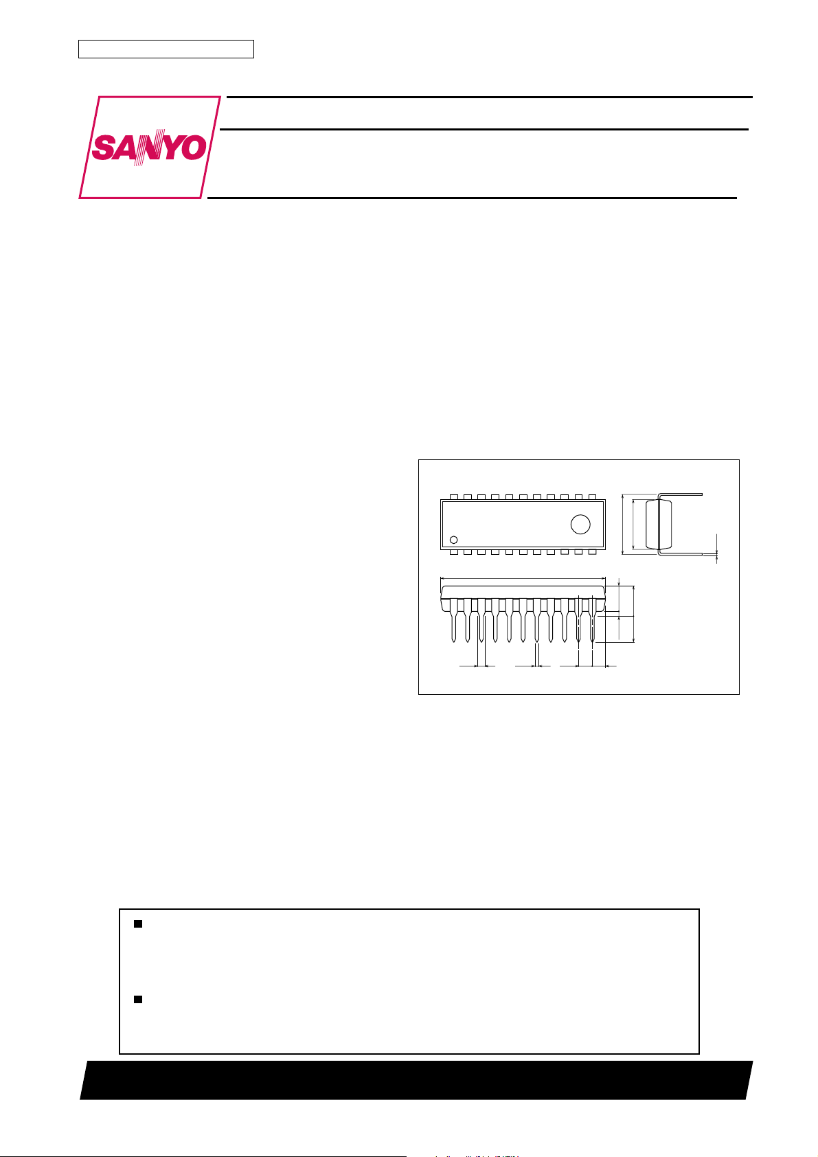
Package Dimensions
unit:mm
3059-DIP22S
[LA3401]
22 12
6.4
7.62
111
21.2
3.25
3.9max
3.3
0.51min
0.95 0.48
1.71.78
SANYO : DIP22S
0.25
12800TH (KT)/41594HK/O077KI/6066KI/6195KI, TS No.1868–1/15
Page 2

LA3401
Specifications
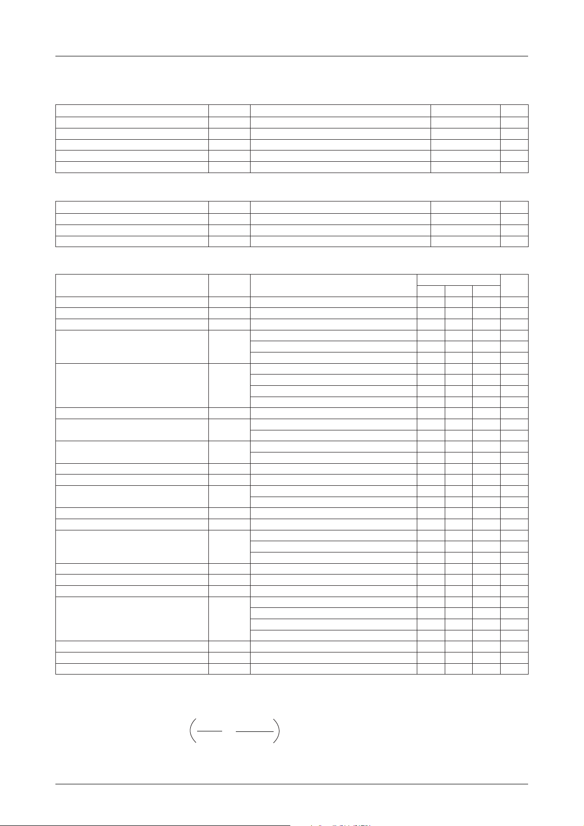
Absolute Maximum Ratings at Ta = 25˚C
retemaraPlobmySsnoitidnoCsgnitaRtinU
egatloVylppuSmumixaMV
tnerruCgnivirDpmaLI
noitapissiDrewoPelbawollAxamdP 026Wm
erutarepmeTgnitarepOrpoT 07+ot02–
erutarepmeTegarotSgtsT 521+ot04–
Operating Conditions at Ta = 25˚C
retemaraPlobmySsnoitidnoCsgnitaRtinU
egatloVylppuSdednemmoceRV
egatloVlangiStupnIdednemmoceRiV 004ot003Vm
egnaRegatloVgnitarepOV
Operating Characteristics at Ta = 25˚C, VCC=13V, f=1kHz, input 400mV, L+R=90%, pilot=10%
retemaraPlobmySsnoitidnoC
tnerruCtnecseiuQoccItnecseiuQ5253Am
ecnatsiseRtupnIirtupniMA,MF4102k
ylppuSrewoPfonoitcejeRelppiR 43Bd
noitarapeSlennahCpeS
noitrotsiDcinomraHlatoTDHT
leveLtupnIelbawollAxamniV)MA,onomMF(%1=DHT008Vm
N/S
)1*(egatloVtuptuOoV
ecnalaBlennahCBCMA,onoM 1Bd
noitaunettAgnituMetumttAFFOetumlanretxE0797Bd
klatssorCTC
egatloVNO-etuMnotmVegatlov51niP5.3V
egatloVFFO-etuMffotmVegatlov51niP 3.0V
egatloVrevoegnahCMA/MFV
egatloVpotSOCV egatlov71niP0.5V
kaeLreirraCzHk9191LCsisahpme-eD33Bd
kaeLreirraCzHk8383LCsisahpme-eD64Bd
etumlanretxE(egatloVtuptuOCDninoitairaV
FFO
leveLgnithgiLpmaLtoliP 4871Vm
siseretsyHpmaL 3Bd
egnaRerutpaCVm03toliP2.1±%
(Note) *1 : The signal voltage after separation adjust is measured.
*2 : The maximum voltage applied to pin 10 (FM/AM changeov er v oltage) is set to VCC–2V (not exceeding 10V).
*3 : Capture range is defined by :
xam 0.61V
CC
xam 0.03Am
L
Ta≤45˚C
CC
po 0.41ot5.6V
CC
nimpytxam
zH001=f54Bd
zHk1=f0455Bd
zHk01=f05Bd
onoM10.080.0%
niamoeretS520.01.0%
busoeretS20.01.0%
MA10.080.0%
k1.5=gR,Vm003,onoM Ω FPL,19Bd
k1.5=gR,Vm004,onoM Ω FPL,0849Bd
Vm003tupnI,MA,onoM20826115451Vm
Vm004tupnI,MA,onoM070105510602Vm
MA → MF5627Bd
MF → MA5627Bd
MA,egatlov01niP → MF5.0V
MA-MF
MF,egatlov01niP → MA3.401V
oerets-onoM53041Vm
etum-onoM51011Vm
etum-oeretS53041Vm
etum-MA51011Vm
0.31V
sgnitaR
3–V
CC
VCC2–V
2–V
CC
˚C
˚C
tinU
Ω
Capture range = – × 100 [%]
F0–F1F1F0–456
456
Where F0 : Free-running frequncy
F1 : Capture frequency when input frequency is changed.
No.1868–2/15
Page 3

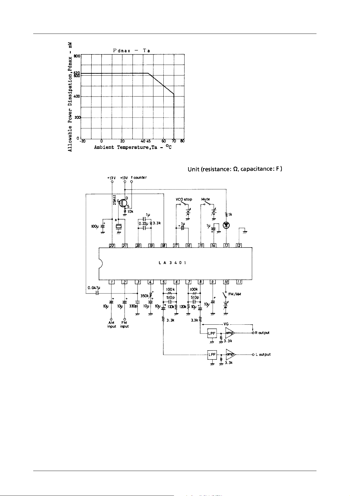
Test Circuit
LA3401
* : CSB456F 11typ (Murata)
LPF : BL-13 (Korin Giken)
amp : THE=0.005% max, VNI=1µV max, band width : 100kHz min, ri=330kΩ max.
VG : S/N, muting attenuation, crosstalk measurement=50dBmin, Other measurements than above=0dB
No.1868–3/15
Page 4

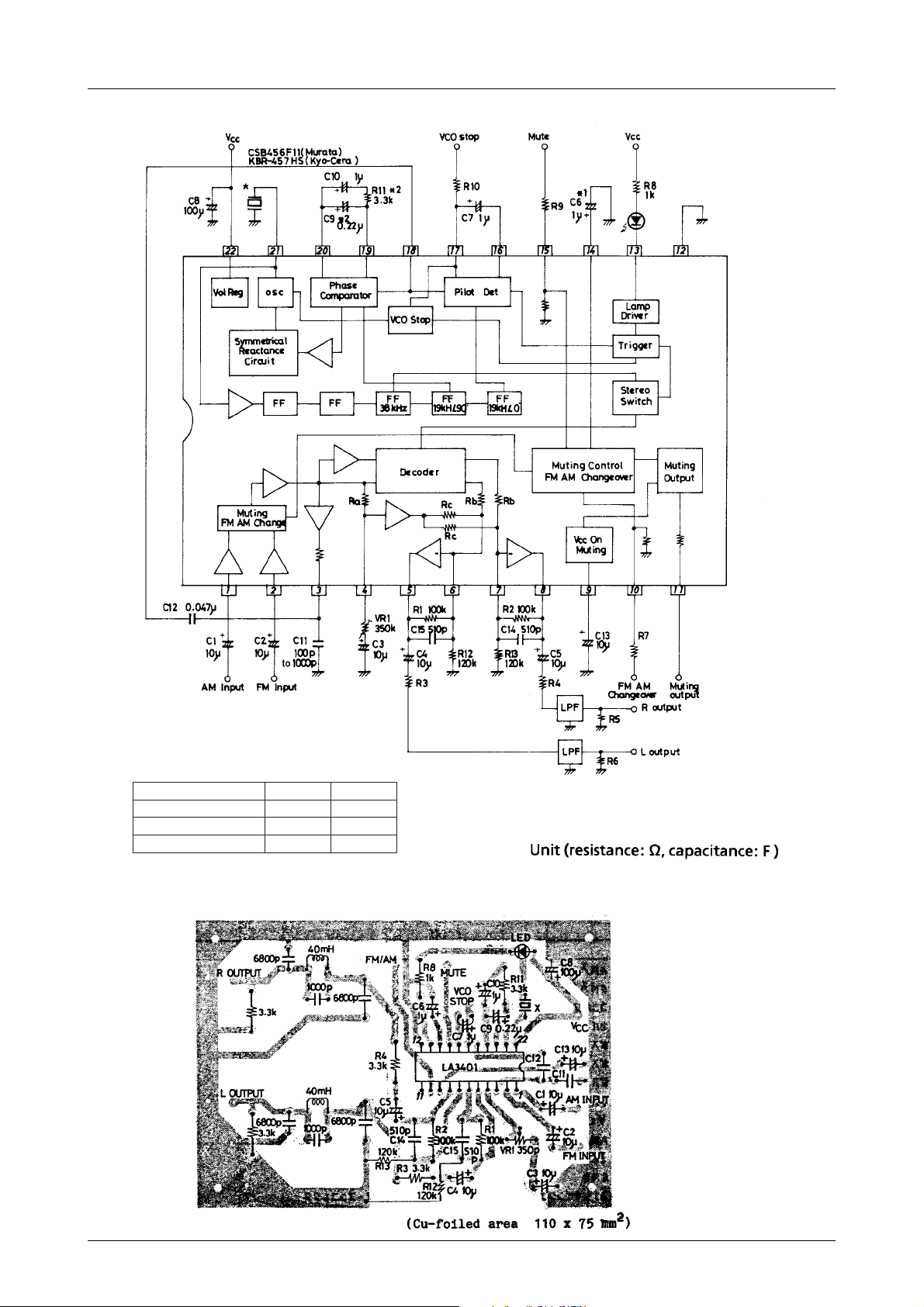
Sample Application Circuit
LA3401
(Note 1) Connect pin 14 to GND through a capacitor of
0.01µF or greater.
(Note 2) For R11, C9, it is recommended to use the
following values according to an IF IC to be
used.
CIFI11R9C
5321ALk3.3µ22.0
N1321,0321,5621ALk6.5µ22.0
0621ALk01µ1.0
* : CBS456F11 (Murata)
KBR-457HS (Kyocera)
Sample Printed Circuit Pattern
No.1868–4/15
Page 5

LA3401
External Parts
.oNtraPnoitpircsiD skrameR
1CtucCD
2CtucCD .seicneuqerfwoltanoitarapessnesroweulavehtgnisaerceD
3CtucCD .seicneuqerfwoltanoitarapessnesroweulavehtgnisaerceD
5,4CtucCD
6CedomrevoegnahctagnitumroftnatsnocemiT roFµ10.0foroticapaca,dedivorpsignitumrevoegnahcMA/MFonnehwnevE
7CretliftcetedecnyS
8CretlifelppirylppusrewoP
9CretlifpoolLLP tuptuonoitaludomedotgnidroccadetcelessiFµ22.0ot1.0morfeulavroticapacA
01CretlifpoolLLP oeretssyaledeulavehtgnisaercni;egnarerutapacsnediweulavehtgnisaerceD
11CnoitrotsidoeretsycneuqerfwolnitnemevorpmI aybrehtohcaehtiwdesahperalangisgnihctiwszHk83redoceddnalangis)R–L(
21CtucCD
31CVtagnitumroftnatsnocemiT
51,41Ctnatsnocsisahpme-eD si)sµ57(sµ05=41C·2R=51C·1Rtahtosdenimretedera51C,41CfoseulavehT
2,1Rtnatsnocsisahpme-edrotsiserkcabdeefreifilpmatsoP )sµ57(sµ05=41C·2R=51C·1R
4R,3RrotsisertupniFPLk3.3 Ω ebtonnacegatalovtuptuomumixameht,sihtnahtsselfI(retaergro
6,5RrotsisertuptuoFPL
7RrotsisergnitimiL eulavasemoceb01nipotdeilppaegatlovtahtosdenimretedsi7RfoeulavehT
8RrotsisergnitimiL .Am03deecxetontsum31nipotnigniwolftnerruC
9RrotsisergnitimiL eulavasemoceb51nipotdeilppaegatlovtahtosdenimretedsi9RfoeulavehT
01RrotsisergnitimiL eulavasemoceb71nipotdeilppaegatlovtahtosdenimretedsi01RfoeulavehT
11RretlifpooL k01ot3.3morfeulavrotsiserA Ω fotuptuonoitaludomedotgnidroccadetcelessi
31,21RgnittesegatlovCDtuptuO .egatlovCDtuptuoreifilpmatsoP
1RVtsujdanoitarapeS .1RVhtiwlevellangis)R+L(gnignahcybdetsujdasinoitarapeS
Xgnittesycneuqerfgninnur-eerF )arecoyK(SH754-RBK,)ataruM(11F654BSC
CC
edomNO- .rewopfonoitacilpparetfaemitniatrecarofdetumsilangistuptuO
.dedleiy
).deniatbo
Note 1 : For C9, R11 setting, refer to Sample Application Circuit (Note 2) and Note 2 for Using IC.
Note 2 : To advance stereo operation start timing, the value of C10 is decreased. Decreasing the value of C10 narrows
capature range. This narrowing also depends on the value of C9. It is recommended to use C10 of 0.47µF or
greater.
.detcennocsiretaerg
)1etoN(.FIMFfo
.potsOCVfoesaelerretfagnimittratsnoitarepo
.detcennoc)tesoiduahcaehtiwsreffid(Fp0001ot001foroticapac
.elbissopsa
VotV3.4morf
CC
VotV5.3morf
.V3–
CC
VotV5morf
.V2–
CC
.)V01gnideecxeton(V2–
.retaldenoitnemnoitacilppapotsOCVotrefer,01RniatbootwohroF
.)2etoN(potsOCVfoesaelerretfagnimittratsnoitarepo
.egnarcimanydtuptuoninoisnetxe,)31R/2R+1(3.3ro)21R/1R+1(3.3
trohssaedamebtsum4Rdna8nipneewtebdna3Rdna5nipneewtebgniriW
oeretssyaledtub,egnarerutapacsnediweulavehtgnisaercnI.)1etoN(FIMF
Pin Voltage, Name Remarks
.oNtraP]V[egatloVemaNniPskrameR
1
2
3
4
5
6
7
8
9
01
11
21
31
41
51
3.3
3.3
3.3
3.3
3.3
3.3
3.3
3.3
3.3
–
–
0
–
–
V
9.4ro0
tupniMA
tupniMF
tuptuoreifilpmaetisopmoC
tsujdanoitarapeS
tuptuoreifilpmatsoP
tupnireifilpmatsoP
tupnireifilpmatsoP
tuptuoreifilpmatsoP
CC
DNG
gnituM
gnitumNO–
revoegnahcMA/MF
tuptuognituM
rotacidnioeretS
etumrevoegnahC
k02rotsisertupnI Ω
k02rotsisertupnI Ω
k1rotsisertuptuO Ω
tuptuoL
tupnisuniM
tupnisuniM
tuptuoR
k08rotsisertupnI Ω
rotcellocnepO
retaergroFµ10.0foroticapacahguorhtdnG
k08rotsisertupnI Ω
Continued on next page.
No.1868–5/15
Page 6

LA3401
Continued from preceding page.
.oNtraP]V[egatloVemaNniPskrameR
61
71
81
91
02
12
22
Note for Using IC
1. Ceramic resonator
(1) Shown below are ceramic resonators recommended for use in the LA3401.
Type No. Supplier
CSB456F11 Murata
KBR-457HS Kyocera
(2) By externally connecting a capacitor in parallel with a ceramic resonator, ceramic resonators shown below can be
also used.
Ceramic resonator Parallec external capacitor
CSB456F10 (Murata) 20pF
KBR-457HS1 (Kyocera) 15pF
2. Capture range and PLL loop filter constants
(1) It is desirable that the capture range, which is related to the stereo distortion, should be set in the range where the
capture range does not depend on the pilot level. For example, when the PLL loop filter constants are C9=0.22µF,
C10=1µF, R11=3.3kΩ, the capture range characteristic becomes as shown in Fig. 1. For these loop filter constants,
it is desirable that the input pilot level should be approximately 20mV or greater where the capture range does not
depend on the pilot level. Figs. 2, 3 shows how the capture range characteristic changes with the loop filter constants.
7.2
7.2
7.2
7.2
7.2
–
V
CC
tupniLLP
r0etlifpooL
retlifpooL
CSO
retliftcetedcnystoliP
potsOCV,retliftcetedcnystoliP
V2.4–
ulppusrewoP
V5.2–
No.1868–6/15
Page 7

LA3401
(2) Fig. 5 shows how the capture range changes with
loop filter constant R11.
(3) Fig. 6 shows how the distortion of stereo main (L +
R) changes with loop filter C9.
3. VCO stop method
The relation between VCO stop supply VS and limiting
resistor RS is shown in Fig. 7. RS must be set so that the
voltage on pin 17 is within the specified range when V
is applied. For example, it is seen from Fig. 7 that the
value of RS is approximately 33kΩ when the voltage on
pin 17 is set to 7V at VS=12V. The relation between R
and the voltage on pin 17 at the VCO stop mode is shown
in Fig. 8. The voltage on pin 17 at the VCO stop mode
increases with increasing RS. The lower v alue on pin 17
is set by adding an increase in the voltage to the minimum value specified.
S
S
No.1868–7/15
Page 8

4. Forced monaural mode
To provide the forced monaural mode, pin 16 is connected to GND through a resistor of 10kΩ. In this case,
VCO oscillation does not stop.
FM/AM mode changeover
(1) How to change over
Changeover is performed by externally applying voltage to pin 10.
FM → AM changeover : Apply a voltage of 4.3V to
VCC–2 (not exceeding 10V) to pin.
AM → FM changeover : Apply a voltage of 0.5V or less
to pin 10.
Fig. 9 shows the relation between the voltage on pin 10
and the flow-in current.
LA3401
(2) Muting in the changeover mode
Muting is turned ON for a certain period of time fixed
by external capacitor C6 in the FM → AM or AM →
FM changeover mode (muting in the changeover mode).
Fig. 10 shows the relation between the muting time in
the chageover mode and C6.
(3) VCO oscillation stop in the AM mode
By externally applying a specified voltage to pin 10 to select the AM mode, VCO oscillation stops automatically and
the monaural mode is forced to be entered.
Muting function
(1) How to turn ON/OFF muting
Muting is turned ON/OFF by externally applying voltage to pin 15.
Muting ON : Apply a voltage of 3.5V to VCC–3V to pin 15.
Muting OFF : Apply a voltage of 0.3V or less to pin 15.
Fig. 9 shows the relation between the voltage on pin 15 and the flow-in current.
(2) Hysteresis characteristic
Muting ON/OFF is allowed a hysteresis of approximately 6dB to prevent malfunction attributable to ripple included in the IF meter output, muting drive output.
(3) Forced monaural in the muting mode
By externally applying a specified voltage to pin 15 to select the muting mode, the forced monaural mode is
automatically entered.
No.1868–8/15
Page 9

LA3401
Muting output
Since the muting signal is delivered at the muting output (pin 11) in the following mode, e xternal transistors can be
used to provide external muting.
¡ AM → FM changeover mode (muting in the changeover mode)
™ Muting mode
£ VCC–ON/OFF mode
Fig. 11 shows a sample application of external muting.
Muting in the VCC-ON mode
1. Muting time
Muting is turned ON for a certain period of time fixed
by external capacitor C13. Fig. 12 shows the relation
between the muting time and C13.
2. Values of AM/FM input coupling capacitors (C1, C2) and value of C13
If muting is released before the DC voltage on the AM input (pin 1) or FM input (pin 2) is stabilized after VCC is
turned ON, pop noise is generated. Therefore, the value of C13 must be determined by the input coupling capacitor
value. The adequate value of C13 for C1, C2 of 10µF is 10µF or thereabouts. If the value of C1, C2 is increased, the
value of C13 is also increased accordingly.
Feedback resistance of post amplifier and total gain, de-emphasis constant values
Table 1 shows the feedback resistance of post amplifier and total gain, de-emphasis
Table 1. Feedback resistance of post amplifier and total gain, de-emphasis
)2R(1RlatoTsµ05)41C(31Csm05)41C(31C
k33 Ω
k93 Ω
k15 Ω
k26 Ω
k28 Ω
k001 Ω
k031 Ω
k051 Ω
k081 Ω
Bd0.3
Bd5.4
Bd5.6
Bd5.8
Bd0.11
Bd0.31
Bd0.51
Bd0.61
Bd5.71
Fp0051
Fp0021
Fp0001
Fp057
Fp026
Fp015
Fp093
Fp033
Fp072
Fp0022
Fp0002
Fp0051
Fp0021
Fp019
Fp057
Fp065
Fp015
Fp093
Total gain : Value in monaural mode
R1 · C15=R2 · C14=50µs, 75µs
No.1868–9/15
Page 10

LA3401
How to externd the dynamic range of the post amplifier
In the Sample Application Circuit of the LA3401 the dynamic range of the post amplifier is extended by connecting
resistors R12, R13 across the virtual GND points (pins 6, 7) of the post amplifier and GND as shown in Fig. 13 to set
the output (pins 5, 8) DC voltages to an adequate value.
The DC voltages on pins 5, 8 are obtained as follows :
3.3
3.3
RB + R1
R
B
RB + R2
R
B
=3.3 1+
=3.3 1+
R1
R
R2
R
B
B
The upper and lower loss voltages of the post amplifier output
are approximately 2V and 0.5V respectively as shown in Fig.
14. With these loss voltages considered, the voltages on pins
5, 8 are set.
In the Sample Application Circuit the voltages on pins 5, 8 are
set to 6V and the maximum output voltage is obtained at
VCC=13V.
The Sample Application Circuit provides the reduced
voltage characteristic at approximately 9V. If the reduced
voltage characteristic at approximately 6V is required,
remove R12, R13 shown in the Sample Application
Circuit. Then, the output (pins 5, 8) DC voltages becomes
approximately 3.3V and the reduced voltage characteristic
becomes as shown in Fig. 15. Fig. 15 shows the THD vs.
VCC characteristic, but other characteristics such as
separation are also available at VCC=6V by removing
R12, R13.
Low-pass filter
Fig. 16 shows a sample circuit configuration where an
LC filter is used as the low-pass filter and Fig. 17 shows
a sample characteristic of this filter. As compared with the LPF (BL-13) in the Sample Applicatin Circuit, the use of
this filter makes the attenuation less at 19kHz, 38kHz : therefore, carrier leak at the LPF output causes the stereo
distortion and separation characteristic to get worse than specified in the Operating Characteristics. For the stereo
distortion, the BL-13 provides approximately 0.02%, while the LC filter provides approximately 0.5%.
No.1868–10/15
Page 11

LA3401
Decorder circuit (Refer to the Block Diagram in the Sample Application Circuit.)
The LA3401 adopts a decoder circuit of chopper type. The sub signal syncdetected by this decoder is applied to the post
amplifier minus input through Rb as shown in the Sample Application Circuit. This signal is matrixed with the main
signal coming out of amplifier A5 and passing through RC.
The gain for the sub signal is :
R1Rb2
VS · or VS ·
The gain for the main signal is : VR1 : Semifixed resistor for separation adjust
VR1
VM · or VM ·
Ra + VR1R1Rc
In the LA3401, the gain of the main signal is varied with VR1 to adjust the separation. Since the IF output is generally
such that the sub signal level is lower than the main signal level, the separation can be adjusted by attenuating the main
signal level with VR1. The use of an antibirdie filter across the IF output and the FM input of the LA3401 may cause the
sub signal level to be raised, and when the sub signal level is higher than the main signal level the separation cannot be
adjusted with VR1. In this case, the sub signal level is attenuated to be less than the main signal level and applied to the
LA3401 and the separation is adjusted with VR1.
π
R2Rb2
π
VR1
Ra + VR1R2Rc
R1, R2 : Post amplifier feedback resistor
VS : Peak value of input sub signal
VM : Peak value of input main signal
No.1868–11/15
Page 12

LA3401
No.1868–12/15
Page 13

LA3401
No.1868–13/15
Page 14

LA3401
No.1868–14/15
Page 15

LA3401
Specifications of any and all SANYO products described or contained herein stipulate the performance,
characteristics, and functions of the described products in the independent state, and are not guarantees
of the performance, characteristics, and functions of the described products as mounted in the customer's
products or equipment. To verify symptoms and states that cannot be evaluated in an independent device,
the customer should always evaluate and test devices mounted in the customer's products or equipment.
SANYO Electric Co., Ltd. strives to supply high-quality high-reliability products. However, any and all
semiconductor products fail with some probability. It is possible that these probabilistic failures could
give rise to accidents or events that could endanger human lives, that could give rise to smoke or fire,
or that could cause damage to other property. When designing equipment, adopt safety measures so
that these kinds of accidents or events cannot occur. Such measures include but are not limited to protective
circuits and error prevention circuits for safe design, redundant design, and structural design.
In the event that any or all SANYO products(including technical data,services) described or
contained herein are controlled under any of applicable local export control laws and regulations,
such products must not be exported without obtaining the export license from the authorities
concerned in accordance with the above law.
No part of this publication may be reproduced or transmitted in any form or by any means, electronic or
mechanical, including photocopying and recording, or any information storage or retrieval system,
or otherwise, without the prior written permission of SANYO Electric Co. , Ltd.
Any and all information described or contained herein are subject to change without notice due to
product/technology improvement, etc. When designing equipment, refer to the "Delivery Specification"
for the SANYO product that you intend to use.
Information (including circuit diagrams and circuit parameters) herein is for example only ; it is not
guaranteed for volume production. SANYO believes information herein is accurate and reliable, but
no guarantees are made or implied regarding its use or any infringements of intellectual property rights
or other rights of third parties.
This catalog provides information as of January, 2000. Specifications and information herein are subject
to change without notice.
PS No.1868–15/15
 Loading...