

Page 1
Ordering number : ENN2564B
22502TN (OT)/10700TH (KT)/O147TA, TS No. 2564-1/15
Overview
The LA3241 is a preamp IC for compact cassette player
recording-only use. The distinctive feature of the LA3241
is that it contains mechanical switches which have been so
far connected externally as peripheral parts.
Applications
• Radio-cassette tape recorder/tape deck-use stereo
compact cassette player.
Features
• Wide ALC : ALCW=60dB typ.
• 2-step ALC level : ALCVo=0.42V, 0.65V.
• On-chip electronic select switches permitting selection
of normal/metal tape and normal/higher speed mode
recording equalizer.
• On-chip mike amp : Gain 25dB typ fixed.
• Low-voltage operaton because the Schottky barrier
diode is used for ALC rectifier diode.
• Wide operating voltage : VCC=4.5 to 14.0V.
Functions
• Recording preamp ×2
• Mike amp ×1
• ALC ×1
• Electronic switch ×6
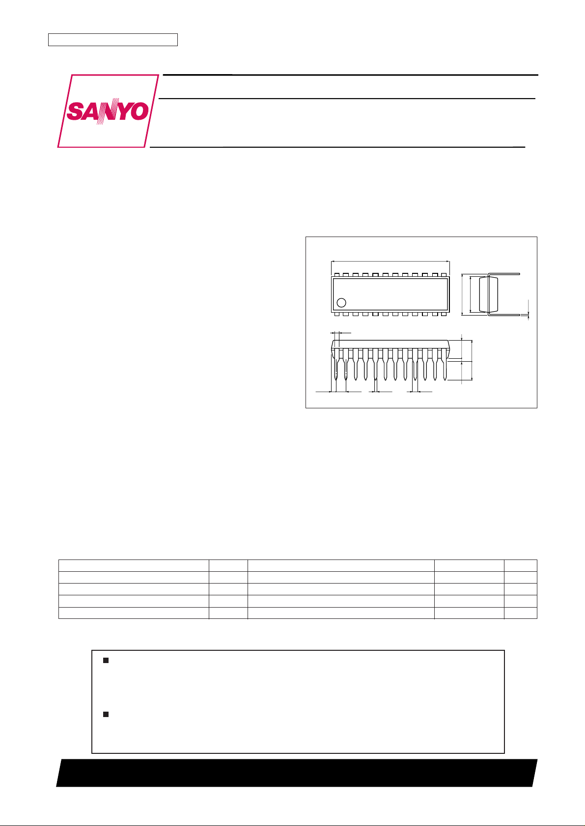
Package Dimensions
unit: mm
3067A-DIP24S
0.48
(3.25)
3.3
3.9max
0.51min
21.0
(0.71)
1.78
0.25
7.62
6.4
1
12
24
13
0.95
0.9
SANYO: DIP24S (300 mil)
[LA3241]
LA3241
SANYO Electric Co.,Ltd. Semiconductor Company
TOKYO OFFICE Tokyo Bldg., 1-10, 1 Chome, Ueno, Taito-ku, TOKYO, 110-8534 JAPAN
Preamplifier for
Compact Cassette Recording-Only Use
Monolithic Linear IC
Any and all SANYO products described or contained herein do not have specifications that can handle
applications that require extremely high levels of reliability, such as life-support systems, aircraft’s
control systems, or other applications whose failure can be reasonably expected to result in serious
physical and/or material damage. Consult with your SANYO representative nearest you before using
any SANYO products described or contained herein in such applications.
SANYO assumes no responsibility for equipment failures that result from using products at values that
exceed, even momentarily, rated values (such as maximum ratings, operating condition ranges, or other
parameters) listed in products specifications of any and all SANYO products described or contained
herein.
Parameter Symbol Conditions Ratings Unit
Maximum Supply Voltage V
CC
max 16 V
Allowable Power Dissipation Pd max 720 mW
Operating Temperature Topr –20 to +75 °C
Storage Temperature Tstg –40 to +125 °C
Specifications
Maximum Ratings at Ta = 25°C
Page 2
No. 2564-2/15
LA3241
Parameter Symbol Conditions
Ratings
Unit
min typ max
Quiescent Current I
CCO
Me/Nor, Nor/High SW off 5 7.5 12 mA
Quiescent Current I
CCS
Me/Nor, Nor/High SW on 10 15 20 mA
[REC Amp]
Voltage Gain (Open) VG
O1
75 85 dB
Voltage Gain (Closed) VG1 VO=0dBm 41.5 43.5 46.0 dB
Total Harmonic Distortion THD1 VO=0.4V 0.1 0.7 %
Maximum Output Voltage V
O
max THD=1% 0.7 1.0 V
Equivalent Input Noise Voltage V
NI1
Rg=2.2kW, BPF : 20Hz to 20kHz 1.2 1.8 µV
Input Resistance Ri1 40 50 60 kΩ
Crosstalk
CT1 Between REC amps 50 70 dB
CT2 REC amp → Mike amp 60 80 dB
Channel Balance CB Vi=–50dBm 0 2 dB
[Mike Amp]
Voltage Gain VG
O2
40 50 dB
Voltage Gain VG2 VO=0dBm 23 25 27 dB
Total Harmonic Distortion THD2 VO=0.4V 0.1 0.7 V
Maximum Output Voltage VO2 THD=1% 0.8 1.1 V
Equivalent Input Noise Voltage VNI2 Rg=2.2kΩ, BPF : 20Hz to 20kHz 1.2 1.7 µV
Input Resistance Ri2 40 50 60 kΩ
Crosstalk CT3 Mike amp → REC amp 45 60 dB
[ALC]
ALC Range ALC
W
Input range when output distortion becomes
45 55 dB
1% aftrer ALC begins to be applied.
ALC Balance ALC
B
Output difference between CH1 and CH2. 0 2 dB
ALC Distortion ALC
THD
Vi=–40dBm 0.15 0.80 %
ALC Output Voltage ALC
Vo
Vi=–40dBm, pin 17 Gnd 0.37 0.46 0.57 V
Vi=–40dBm, pin 17 open 0.6 0.7 0.85 V
Crosstalk CT4 Between REC amps 45 60 dB
CT5 REC amp → Mike amp 50 70 dB
[Switch]
On-State Resistance R
ON
30 70 Ω
DC Feedback Resistance R
F1
40 50 60 kΩ
Operating Characteristics at Ta = 25°C, VCC= 6 V, RL= 10kΩ, f = 1 kHz, 0dB = 0.775 V
Parameter Symbol Conditions Ratings Unit
Recommended Supply Voltage V
CC
6 V
Operating Voltage range V
CC
op 4.5 to 14.0 V
Recommended Operating Conditions at Ta = 25°C
Page 3
No. 2564-3/15
LA3241
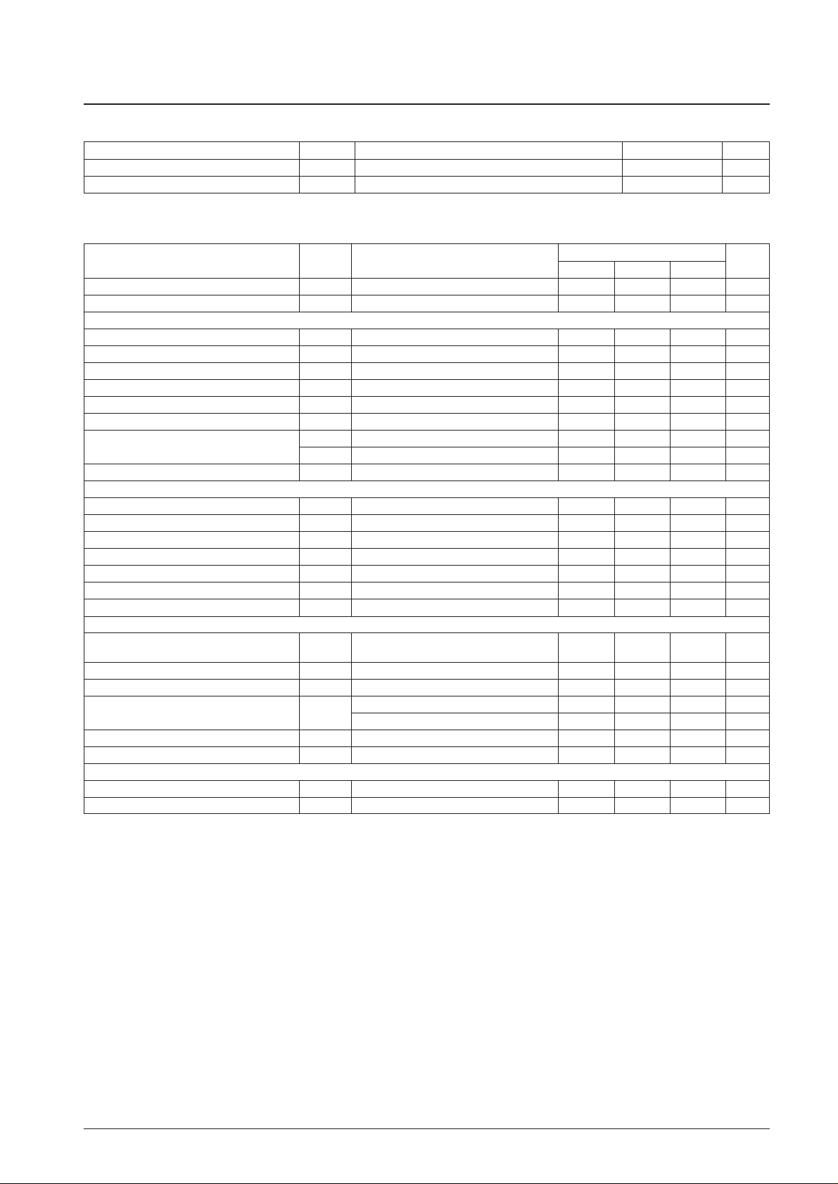
Equivalent Circuit Block Diagram
24 23 22 21
20
19
18
17
16
15
14
13
1 2 3 4 5 6 7 8 9 10 11 12
3.6kΩ3.6kΩ
50kΩ
50kΩ
50kΩ
50kΩ
10kΩ
50kΩ
IN2 NF2 OUT2 RFC V
CC
Nor / High
OUT2
Me / Nor
OUT2-1
Me / Nor
OUT2-2
ALC
IN2
ALC
CONT
Nor / HighSWMIC
OUT
IN1 NF1 OUT1 MICINGNDNor / High
OUT1
Me / Nor
OUT1-1
Me / Nor
OUT1-2
ALC
IN1
ALC Me / NorSWMIC
NF
+
--
--
--
+
+
preamp1
preamp2
ALC
MIC
SBD
Me / Nor SW
SBD
Nor / High
Speed
ILA00602
R
F
Top view
Equivalent Circuit
1
24 23
2 3 4 5 6 7 8 9 10 11 12
TR18
High
Speed
Charge
TR12
TR11
TR10TR9
TR8
TR1
TR7
TR5
TR2
TR3 TR4
TR6
TR14
TR13
TR15TR16
TR17
VR2
3.6kΩ
50kΩ
VR1
D1D2
D4 D5
TR9
50kΩ
10kΩ
100µA
100Ω
50Ω
50kΩ
50kΩ
50kΩ
3.6kΩ
50Ω
10kΩ
10kΩ
100Ω
22 21
20 19 18 17 16 15 14 13
ILA00603
--
~
Page 4
No. 2564-4/15
LA3241
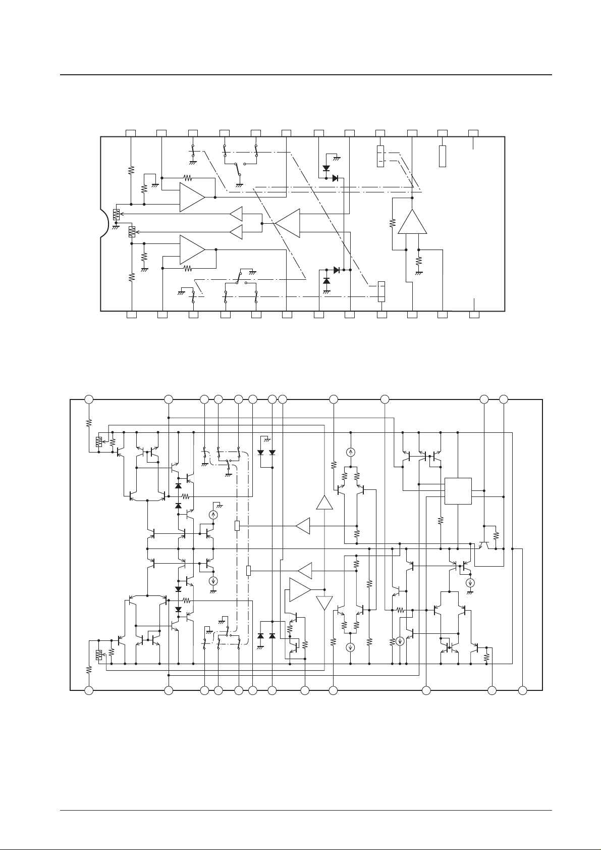
Test Circuit Diagram
24123222321420519
6
1781691510141113
12
S14
S13
S4 1/2
SW4
VNF2V
NFS
2 VO2 MIC OUT
2
21
S9
S1
S11
S10
I
CC
V
CC
GND
1 2
2 1
2
1
2
1
+
+
+
+
+
+
+
+ + +
+
+
+ +
+
+
+
1µF
1µF
47µF
47µF
220µF
4.7µF
4.7µF
4.7µF
100µF
100µF
8.2kΩ
100kΩ
1µF
300Ω
300Ω
300Ω
300Ω
8.2kΩ
100kΩ
1µF
470kΩ
220µF
4.7µF
100µF
16kΩ
2.2kΩ
680Ω
10µF
10kΩ
300Ω
300Ω
300Ω
300Ω
10kΩ
10kΩ
10kΩ
2
S3
1
1
VIN1
VNF1V
NFS
1 VO1
2
2
1
1 2
2
S5
S6
MIC IN
S7
S8
1
1 2
2 1 2 1
1
2/2
1/2
2/2
A
7
18
LA3241
ILA00604
Top view
Page 5
No. 2564-5/15
LA3241
Sample Application Circuit
23
100kΩ
22 21
20
19
18
17 15 14
13
1 2 3 4 5 6 7 8 10 12
+
+ +
+ +
+
+
bias
Z3
Z2
Z1
ILA00605
SW(10)
Level select
V
CC
V
CC
V
CC
100µF
4.7µF
4.7µF
47µF
0.7V
OFF
0.46V
ON
100µF
PB Amp IN
8.2kΩ
300Ω
radio
OUT
radio
OUT
100kΩ
10kΩ
1µF
bias
Z3
Z2
Z1
V
CC
47µF
PB Amp IN
8.2kΩ
470kΩ
10kΩ
680Ω
300Ω
1µF
V
CC
4.7µF
4.7µF
10µF
100µF
MIC
SW(9)
+
+
+
+ +
++
9
16
3.6kΩ
3.6kΩ
50kΩ
50kΩ
50kΩ
50kΩ
10kΩ
50kΩ
+
+
--
--
preamp1
preamp2
ALC
RF
SBD
SBD
Me / Not SW
SBD
SBD
Nor / High
Speed
MIC
24
11
Top view
(Notes)
1. The electronic select switch level is approximately (VCC–0.9)/2.
2. REC amplifier NF parameters Z1 through Z3 should be selected to accommodate the recording level and frequency
response that will be required in metal/normal tape and normal/higher speed modes.
3. Z1 through Z3 may be configured with coil “L”, capacitor “C”, and resistor “R”.
4. The electronic select switch mode illustrated above shown no VCCbeing impressed on Me/Nor SW⑨ or Nor/High
SW⑩.
5. The ALC level on pin 7 should not be changed over while VCCis impressed.
Page 6

Usage Notes
No. 2564-6/15
LA3241
(1) Input pins 1 and 24 have internal resistors of 3.6 kΩ (typical) inserted.
50kΩ
3.6kΩC
ILA00607
24
1
When applying external voltages to input pins 1 and 24, insert
capacitors in the input. We recommend capacitances in the range
0.1 to 10 µF. The DC voltage V
IN DC
when pins 1 or 24 is left
open will be 50 mV or lower.
(V
IN DC
= 20 mV typical)
See the VCC– V
IN DC
Characteristics for the supply voltage V
CC
and V
IN DC
characteristics.
(2) Output waveform starting time
ILA00608
SW
200Ω
3kΩ
Cr
V
CC
+
ILA00609
VCC on
t
s
When the supply voltage VCCis applied, the amplifier outputs (pins 6 and 19) start up. The output waveform turn-on
time, ts, can be modified by adding the capacitor Cr to pin 12. The minimum value for Cr is 33 µF. Values smaller
than this will aggravate the power-on impulse noise and degrade the ripple rejection ratio. At Cr = 100 µF, ts will be
0.7 s, typical.
(3) Electronic switch control circuit
ILA00610
V
CC
4µAmin
300µA
1kΩ
1kΩ
100Ω
200Ω
R1=R2
R2
3kΩ
0.9V
R1
+
--
~
--
~
--
~
14
13
9
16
The control pin (pins 9 and 16) switching circuit has the
structure shown in the figure. The control circuit switching
level, V
CONT
, is given by the following formula.
V
CONT
= 1/2 × (VCC– 0.9) [V]
Page 7

No. 2564-7/15
LA3241
(4) Relationship between the electronic switch on and off control voltage levels and the power supply voltage
(See VCC– V
CONT
for the data.)
Pin9,16(V)
VCC(V)
V
CONT
ILA00611
When the supply voltage VCCis determined, the corresponding
electronic switch control pin (pins 9 and 16) control levels will be
determined. There is a threshold area of about 1 V. The center
point of the threshold area for a given supply voltage VCCwill be
roughly:
1/2 × (VCC– 0.9) [V]
Therefore, the electronic switches can be turned on and off
reliably by applying voltages that are at least ±0.5 V of this center
point voltage to the electronic switch control pins (pins 9 and 16).
(5) Add a 470 pF capacitor between pin 15 and ground to prevent oscillation at low temperature in the microphone
amplifier output.
ILA00612
input
50kΩ
10kΩ
output
470pF
+
+
--
11
10
15
(6) The ALC switching level can be implemented with pin 7. The IC supply voltage VCCmust be turned off temporarily
when switching to prevent ALC failure.
50Ω
SBD × 4
ALC Drive
50Ω
TR2
TR1
ILA00613
18
7
8 17
(7) Although the ALC level is converted by opening (0.7 V) or shorting (0.46 V) pin 17, basically, the ALC start DC
threshold level is switched by turning transistor TR2 on (pin 17 open) or off (pin 17 shorted).
Rectifier Block Equivalent Circuit
Page 8

No. 2564-8/15
LA3241
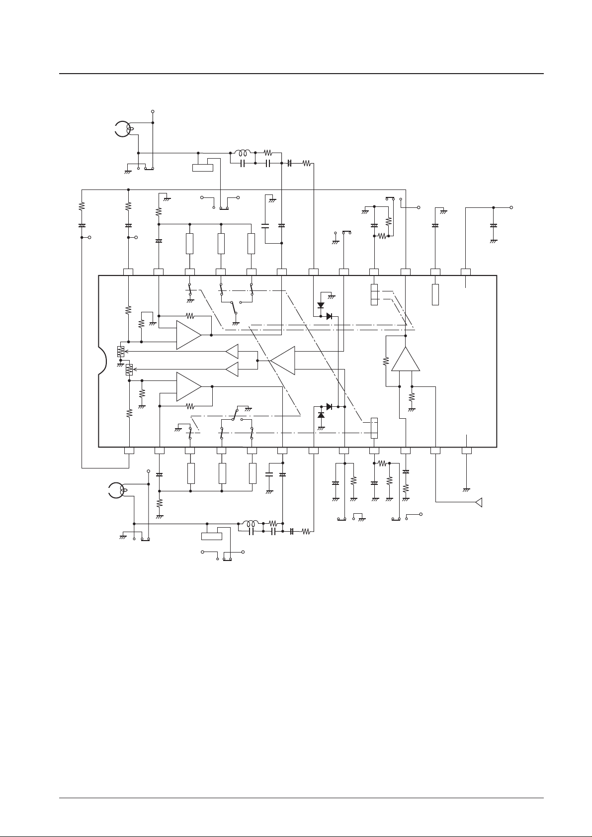
LA3241 and LA3246 Cassette Dubbing System Circuit Example
Radio
10k
Ω
10
µ
F
100
µ
F
100
µ
F
100k
Ω
47
µ
F
47
µ
F
Pre a
2
Mix
0dB
Pre a
1
R2
F2
P
P
F1
R1
180
Ω
100k
Ω
4.7
µ
F
0.01µF
2k
Ω
300k
Ω
Tape A
Tape A
300k
Ω
Tape
PB
1
µ
F
8.2k
Ω
4.7
µ
F
4.7µF
RF
10k
Ω
100k
Ω
10k
Ω
50k
Ω
10k
Ω
100
µ
F
0.46V
0.7V
on
300
Ω
47
µ
F
50k
Ω
50k
Ω
8.2k
Ω
470k
Ω
50k
Ω
47
µ
F
PB REC
PB REC
V
CC
4.7
µ
F
10
µ
F
4.7
µ
F
1
µ
F
ALC Met
ECM
ILA00614
Nor
off on
100
µ
F
100k
Ω
680
Ω
1µF
300
Ω
3.6k
Ω
1µF
50k
Ω
ALC
off
ALC
REC
V
CC
Bias
PB
R / P
R / P
TapeB
TapeB
PB
3.6k
Ω
Pre a 2
Pre a 1
REC
REC
Radio
Dubbing
High / Nor
LA2000
Level
Sensor
Nor High
180
Ω
0.01µF
12k
Ω
2.7k
Ω
0.047µF
47
µ
F
4.7
µ
F
4.7
µ
F
18k
Ω
12k
Ω
10k
Ω
4.7
µ
F
10k
Ω
100k
Ω
2.7k
Ω
0.047µF
PB
Tape
Radio
Dubbing
LA3246
F / R
F
R
Met / Nor
Nor / High
Speed
Nor / High
Speed
LA3241
MIC
Met / Nor
on
18k
Ω
12k
Ω
off
Nor Met
V
CC
IFout=10mA max
VO=V
CC
--1(V
)
V
CC
REC
LA4505
SP
L
R
SP
20 19 18 17 16 15 14 13 12 11
10
1
24 23 22 21 20 19 18 17 15 1314
1 2 3 4 5 6 8 9 10 1211
2 3 4 5 6 7 8 9
1/2
1/2
--
--
+
+
+
+
+
+
+
+
+
+
+
+
+
+
+
+
+
+
+
V
O
+
+
+
+
+ +
+
+
×
+
+
--
--
7
Bias
16
Page 9

No. 2564-9/15
LA3241
VO ALC — Ta
VO max — Ta
ILA00619
ILA00621
VGO, VG — f
i
ILA00622
0
3.0
2.0
1.0
5.0
4.0
0
0.6
0.4
0.2
1.0
0.8
VO max — Ta
ILA00617
--20 0 20 40 60 80 100
--20 0 20 40 60 80 100
0
1.0
0.8
0.2
0.6
0.4
0.8
1.0
1.2
1.4
1.6
0.6
0
0.4
0.2
1.4
1.2
20
18
20
22
24
26
28
30
80
90
70
60
50
40
30
--20 0 20 40 60 80 100
--20 0 20 40 60 80 100
2 3 5
100
2 3 5
1k
2 3 5
10k
2 3 5
100k
--20 0 20 40 60 80 100
VO ALC — Ta
VO max — Ta
VG — Ta
ILA00618
I
CCO
— Ta
ILA00616
ILA00615
40 60 80200--20 100
0
10
6
8
2
4
20
18
16
12
38
44
42
40
50
48
46
14
40--20 0 20 10060 80
Rg=3.6kΩ
VI=0
4.5V
6.0V
9.0V
12.0V
V
CC
=16.0V
REC AMP
VO=0dBm
fi=1kHz
REC AMP
THD=1%
fi=1kHz
REC AMP
17short 0.42V
REC AMP
17short 0.65V
VCC=6.0V
VO=0dBm
MIC AMP
THD=1%
fi=1kHz
12.0V
9.0V
6.0V
4.5V
4.5V
12.0V
4.5V
9.0, 6.0V
6.0V
9.0V
V
CC
=16.0V
VCC=16.0V
V
CC
=16.0V, 12.0V
6.0V
4.5V
V
CC
=16.0V
ILA00620
MIC AMP
VO=0dBm
fi=1kHz
9.0V
6.0V
V
CC
=16.0V
4.5V
12.0V
CNF=220µF
Me / Nor & Nor / High SW on
Nor / High & Me / Nor SW off
With either the Me/Nor or the Nor/High switch on
VCC=4.5V
6.0V
9.0V
12.0V
16.0V
12.0V
9.0V
Ambient temperature, Ta — °C
Maximum output voltage, V
O
max — V
Voltage gain (open circuit), VG
O
— dB
Voltage gain (closed circuit), VG — dB
Input frequency, fi — Hz
Ambient temperature, Ta — °C
Ambient temperature, Ta — °C
Quiescent current, I
CCO
— mA
Voltage gain (closed circuit), VG — dB
Ambient temperature, Ta — °C
Ambient temperature, Ta — °C
Ambient temperature, Ta — °C
Ambient temperature, Ta — °C
Maximum output voltage, V
O
max — V
ALC output voltage, V
O
ALC — V
ALC output voltage, V
O
ALC — V
Maximum output voltage, V
O
max — V
Page 10

No. 2564-10/15
LA3241
0
90
80
70
60
50
40
10
20
30
40
50
60
0
2 4 6 8 10 12 14 16 18
2 4 6 8 10 12 14 16
ILA00625
VG — V
CC
CT — V
CC
0
5
10
15
20
25
0 2 4 6 8 10 12 14 16 18 20
ILA00624
I
CCO
, I
CCS
— V
CC
ILA00627
VGO, VG — f
i
ILA00623
10
20
30
40
50
60
70
80
90
2 3 5
100
2 3 5
1k
2 3 5
10k
2 3 5
100k
MIC AMP
VCC=6.0V
VO=0dBm
CNF=220µF
RNF=680Ω
VO= --10dBm
2kΩ
f=1kHz
ALC off
Input frequency
f=1kHz
Rg=3.6k
Ω
Rg=3.6kΩ
Nor / High & Me / Nor SW on
Nor / High & Me / Nor SW off
Me / Nor SW on
Nor / High SW on
ILA00626
--90 --80 --70 --60 --50 --40 --30 --20
10
2
3
5
2
3
5
0.1
3
5
1.0
2
0.01
3
5
2
VO, THD — V
I
ILA00628
0 2 4 6 8 10 12 14 16 18 20
0
1.0
2.0
3.0
4.0
VO max — V
CC
THD=1%
f=1kHz
RL=10k
Ω
f=1kHz
VCC=6.0V
RL=10kΩ
ILA00629
--60 --50 --40 --30 --20 --10 0 10 20
100
2
3
5
2
3
5
1.0
3
5
10
2
0.1
3
5
2
VO ALC, THD — V
I
THD
V
O
ALC
Pin 17: ground
VCC=4.5V
RL=10kΩ
Rg=3.6kΩ
ILA00630
--60 --50 --40 --30 --20 --10 0 10 20
100
2
3
5
2
3
5
1.0
3
5
10
2
0.1
3
5
2
VO ALC, THD — V
I
THD
V
O
ALC
Pin 17: open
VCC=4.5V
RL=10kΩ
Rg=3.6kΩ
CH2→CH1
CH1→CH2
THD
Me / Nor & Nor / High Speed SW off
VGO
0dBm
V
O
Input voltage, VI— dBm
Input voltage, V
I
— dBm
Supply voltage, VCC— V
Input frequency, fi — Hz
Quiescent current, I
CCO
— mA
Quiescent current (with the electronic switch on), I
CCS
— mA
Supply voltage, VCC— V
Input voltage, V
I
— dB
Supply voltage, V
CC
— V
Supply voltage, V
CC
— V
Voltage gain, VG — dB
Crosstalk, CT — dB
Output voltage, V
O
— V
Total harmonic distortion, THD — %
Maximum output voltage, V
O
max — V
Voltage gain (open circuit), VG
O
— dB
Voltage gain (closed circuit), VG — dB
Output voltage, V
O
— V
Total harmonic distortion, THD — %
Output voltage, V
O
— V
Total harmonic distortion, THD — %
Page 11

No. 2564-11/15
LA3241
ILA00631
--70 --40--50--60 --30 --20 --10 200 10
100
2
3
5
2
3
5
1.0
3
5
10
2
0.1
3
5
2
VO ALC, THD — V
I
ILA00633
--70 --40--50--60 --30 --20 --10 200 10
100
2
3
5
2
3
5
1.0
3
5
10
2
0.1
3
5
2
VO ALC, THD — V
I
Pin 17: ground
Nor / High, Me / Nor on
VCC=6V
RL=10kΩ
Rg=3.6kΩ
Pin 17: open
Nor / High, Me / Nor on
VCC=6V
RL=10kΩ
Rg=3.6kΩ
2
THD
V
O
ALC
THD
V
O
ALC
THD
ILA00632
--60 --30--40--50 --20 --10 0 10 20
0.1
7
3
5
2
1.0
7
3
5
2
10
7
3
5
2
VO ALC, THD — V
I
ILA00634
--60 --30--40--50 --20 --10 0 10 20
0.1
7
3
5
2
1.0
7
3
5
2
10
7
3
5
2
VO ALC, THD — V
I
Pin 17: open
VCC=6V
f=1kHz
RL=10kΩ
Rg=3.6kΩ
V
O
ALC
THD
THD
V
O
ALC
ILA00635
--60 --40--50 --30 --20 --10 200 10
5
2
3
10
5
2
3
1.0
5
2
3
0.1
5
3
VO ALC, THD — V
I
Pin 17: ground
Nor / High, Me / Nor on
VCC=9V
RL=10kΩ
Rg=3.6kΩ
ILA00636
--60 --40--50 --30 --20 --10 200 10
5
2
3
10
5
2
3
1.0
5
2
3
0.1
5
3
2
VO ALC, THD — V
I
Pin 17: open
Nor / High, Me / Nor on
VCC=9V
RL=10kΩ
Rg=3.6kΩ
ILA00637
--60 --40--50 --30 --20 --10 200 10
5
2
3
10
5
2
3
1.0
5
2
3
0.1
5
3
2
2
VO ALC, THD — V
I
Pin 17: open
Nor / High, Me / Nor on
VCC=12V
RL=10kΩ
Rg=3.6kΩ
ILA00638
--60 --40--50 --30 --20 --10 200 10
5
2
3
10
5
2
3
1.0
5
2
3
0.1
5
3
VO ALC, THD — V
I
Pin 17: ground
Nor / High, Me / Nor on
VCC=12V
RL=10kΩ
Rg=3.6kΩ
V
O
ALC
THD
V
O
ALC
THD
V
O
ALC
THD
V
O
ALC
Pin 17: ground
VCC=6V
f=1kHz
RL=10kΩ
Rg=3.6kΩ
Input voltage, VI— dBm
Input voltage, V
I
— dBm
Input voltage, VI— dBm
Input voltage, V
I
— dBm
Input voltage, V
I
— dBm
Input voltage, V
I
— dBm
Input voltage, V
I
— dBm
Input voltage, V
I
— dBm
Output voltage, V
O
— V
Total harmonic distortion, THD — %
Output voltage, V
O
— V
Total harmonic distortion, THD — %
Output voltage, V
O
— V
Total harmonic distortion, THD — %
Output voltage, V
O
— V
Total harmonic distortion, THD — %
Output voltage, V
O
— V
Total harmonic distortion, THD — %
Output voltage, V
O
— V
Total harmonic distortion, THD — %
Output voltage, V
O
— V
Total harmonic distortion, THD — %
Output voltage, V
O
— V
Total harmonic distortion, THD — %
Page 12

No. 2564-12/15
LA3241
ILA00642
0 2 4 6 8 10 12 14 16 18 20
3
2
3
5
7
1000
2
100
VNO — V
CC
3
1
2
0
--1
--2
--3
10
7
5
2
1.0
3
7
5
3
2
0 642 8 1210 14 16
ILA00639
0 642 8 1210 18 2014 16
ILA00641
VO ALC — V
CC
VI= --40dBm
VO ALC=0.44V=0dB
f=1kHz
Rg=3.6kΩ
VNI — V
CC
3
1
2
0
--1
--2
--3
0 642 8 1210 14 16
ILA00640
VO ALC — V
CC
VI= --40dBm
VO ALC=0.66V=0dB
f=1kHz
Rg=3.6kΩ
1.4
1.0
1.2
0.8
0.6
0.2
0.4
0
0 642 8 1210 14 16
ILA00646
VO max — V
CC
Rg=3.6kΩ
VG=45dB=177
(VCC=6V)
f=1kHz
10000
5
7
3
2
7
5
3
2
1000
100
7
5
3
2
100
532
1k
32 2 535
10k
2 3
100k
5
ILA00643
VNO — Rg
V
NO
(FLAT)
V
NO
(DIN)
REC AMP
Rg=3.6kΩ
RL=10kΩ
f=1kHz
ILA00644
100 1k 10k
2 3 5 2 3 5 2 3 5
100k
2 3 5
100 1k 10k
32 5 7 32 5 7 2 3 5 7 2 3
10
5
7
7
1.0
2
3
5
3
2
VNI — Rg
REC AMP
VCC=6V
f=1kHz
V
NO
(DIN)
V
NO
(FLAT)
MIC AMP
f=1kHz
THD=1%
RL=10kΩ
1.4
1.0
1.2
0.8
0.6
0.2
0.4
0
ILA00645
VO max — R
L
VCC=6V
f=1kHz
REC AMP
VCC=6V
f=1kHz
THD=1%
V
O
max
V
O
max
V
NI
Load resistance, RL— Ω
Maximum output voltage, V
O
max — V
Maximum output voltage, V
O
max — V
Supply voltage, VCC— V
Supply voltage, VCC— V
Supply voltage, V
CC
— V
ALC output voltage, V
O
ALC — V
ALC output voltage, V
O
ALC — V
Supply voltage, VCC— V
Supply voltage, V
CC
— V
Input signal source resistance, Rg — Ω
Input signal source resistance, Rg — Ω
Equivalent input noise voltage, V
NI
— µV
Output noise voltage, V
NO
— µV
Output noise voltage, V
NO
— µV
Equivalent input noise voltage, V
NI
— µV
Page 13

No. 2564-13/15
LA3241
ILA00650
VNO — V
CC
5
3
7
5
3
2
1.0
2
0.1
7
5
3
2
0.01
10
7
5
2
1.0
3
7
5
3
2
--60 --50 --40 --30 --20 --10
ILA00647
ILA00649
VO, THD — V
I
VNI — V
CC
32
24
28
20
16
12
8
0
4
0 642 8 1210 14 16
ILA00648
VG — V
CC
2 4 6 8 10 12 14 16 18 20
1000
7
5
7
5
3
2
3
2
100
10
7
5
3
2
30
40
50
60
70
80
2 53
100
532 32
100k
5
1k
32 5
10k
2 53
100
532 32
100k
5
1k
3
2 5
10k
2 53
100
532 32
100k
5
1k
32 5
10k
2 53
100
532 32
100k
5
1k
32 5
10k
ILA00651
ILA00653
ILA00652
VNO — Rg
CT — f
i
10
7
1.0
7
5
3
2
5
3
2
VNI — Rg
CT — f
i
MIC AMP
f=1kHz
VCC=6V
RL=10kΩ
V
O
THD
MIC AMP
f=1kHz
RL=10kΩ
VO=0dBm
VG
V
NI
(DIN)
MIC AMP
Rg=2.2kΩ
RL=10kΩ
MIC AMP
Rg=2.2kΩ
RL=10kΩ
2 4 6 8 10 12 14 16 18 20
10
7
3
5
2
100
7
3
5
2
1000
7
3
5
2
V
NO
(FLAT)
V
NO
(DIN)
MIC AMP
VCC=6V
f=1kHz
RL=10kΩ
V
NO
(FLAT)
V
NO
(DIN)
ILA00654
20
30
40
50
60
70
80
90
MIC AMP→REC AMP
VCC=6V
VO=0dBm(MIC OUT)
Rg=3.6kΩ
V
NI
MIC AMP
REC AMP2
REC AMP1
REC AMP2
MIC AMP
VCC=6V
VG=26dB
RL=10kΩ
MIC AMP
REC AMP2
VCC=6V
VO1=0dBm
Rg=3.6kΩ
*ALC off
REC AMP1→
Input frequency, fi— Hz
Crosstalk, CT — dB
Crosstalk, CT — dB
Input frequency, fi— Hz
Supply voltage, VCC— V
Input voltage, V
I
— dBm
Output voltage, V
O
— V
Total harmonic distortion, THD — %
Voltage gain, VG — dB
Supply voltage, VCC— V
Supply voltage, V
CC
— V
Input signal source resistance, Rg — Ω
Input signal source resistance, Rg — Ω
Equivalent input noise voltage, V
NI
— µV
Output noise voltage, V
NO
— µV
Output noise voltage, V
NO
— µV
Equivalent input noise voltage, V
NI
— µV
Page 14

No. 2564-14/15
LA3241
CT — f
i
ILA00655
30
40
50
60
70
80
90
MIC AMP
MIC AMP
REC AMP2
VCC=6V
VI= --40dBm
(REC AMP1)
Rg=3.6kΩ
*ALC on
(0.42V 17short)
REC AMP1→
Me / Nor on, Nor / High on REC AMP2
Me / Nor off, Nor / High off REC AMP2
CT — f
i
ILA00656
30
40
50
60
70
80
90
MIC AMP
MIC AMP
REC AMP2
VCC=6V
VI= --40dBm
(REC AMP1)
Rg=3.6kΩ
*ALC on
(0.65V 17open)
REC AMP1→
Me / Nor off, Nor / High off REC AMP2
2 53
100
532 32
100k
5
1k
32 5
10k
2 53
100
532 32
100k
5
1k
32 5
10k
2 53
100
532 32
100k
5
1k
32 5
10k
CT — f
i
ILA00657
30
40
50
60
70
80
90
MIC AMP
REC AMP1
MIC AMP
REC AMP1
VCC=6V
VO=0dBm
Rg=3.6kΩ
*ALC off
REC AMP2→
2 53
100
532 32
100k
5
1k
32 5
10k
CT — f
i
ILA00659
20
30
40
50
60
70
80
90
MIC AMP
REC AMP1
REC AMP2→
2 53
100
532 32
100k
5
1k
32 5
10k
2 3 5
1.0 10
32
1000
552 3
100
CT — f
i
ILA00658
Rr — V
CC
Rr — Cr
ILA00660
30
2 4 6 8 10 12 14 16 18
ILA00662
--60
--60
--50
--40
--30
--20
--10
--50
--40
--30
--20
--10
40
50
60
70
80
90
MIC AMP
MIC AMP
REC AMP
REC AMP2→
VCC=6V
VI= --40dBm
(REC AMP2)
Rg=3.6kΩ
*ALC on
(0.42V 17short)
Me / Nor off, Nor / High off REC AMP1
Me / Nor on, Nor / High on REC AMP1
VCC=6V
VI= --40dBm
(REC AMP2)
Rg=3.6kΩ
*ALC on
(0.65V 17open)
MIC AMP
Me / Nor on, Nor / High on REC AMP1
Me / Nor off, Nor /
High off REC AMP1
VR= --20dBm
f=100Hz
CR ???
REC AMP
MIC AMP
2 53
100
532 32
100k
5
1k
325
10k
Rr — f
r
ILA00661
--60
--50
--40
--30
--20
--10
0
10
20
MIC AMP
REC AMP
VCC=6V
fr=100Hz
VR= --20dBm
REC
MIC
Me / Nor on, Nor / High on REC AMP2
VCC=6V
VR= --20dBm
No C
R
Ripple frequency, fr— Hz
Ripple rejection ratio, Rr — dB
Ripple rejection ratio, Rr — dB
Ripple filter capacitor, Cr — µF
Input frequency, fi— Hz
Input frequency, f
i
— Hz
Crosstalk, CT — dB
Input frequency, fi— Hz
Input frequency, f
i
— Hz
Supply voltage, V
CC
— V
Input frequency, f
i
— Hz
Crosstalk, CT — dB
Crosstalk, CT — dB
Crosstalk, CT — dB
Ripple rejection ratio, Rr — dB
Crosstalk, CT — dB
Page 15

PS No. 2564-15/15
LA3241
This catalog provides information as of February, 2002. Specifications and information herein are subject
to change without notice.
Specifications of any and all SANYO products described or contained herein stipulate the performance,
characteristics, and functions of the described products in the independent state, and are not guarantees
of the performance, characteristics, and functions of the described products as mounted in the customer’s
products or equipment. To verify symptoms and states that cannot be evaluated in an independent device,
the customer should always evaluate and test devices mounted in the customer’s products or equipment.
SANYO Electric Co., Ltd. strives to supply high-quality high-reliability products. However, any and all
semiconductor products fail with some probability. It is possible that these probabilistic failures could
give rise to accidents or events that could endanger human lives, that could give rise to smoke or fire,
or that could cause damage to other property. When designing equipment, adopt safety measures so
that these kinds of accidents or events cannot occur. Such measures include but are not limited to protective
circuits and error prevention circuits for safe design, redundant design, and structural design.
In the event that any or all SANYO products (including technical data, services) described or contained
herein are controlled under any of applicable local export control laws and regulations, such products must
not be exported without obtaining the export license from the authorities concerned in accordance with the
above law.
No part of this publication may be reproduced or transmitted in any form or by any means, electronic or
mechanical, including photocopying and recording, or any information storage or retrieval system,
or otherwise, without the prior written permission of SANYO Electric Co., Ltd.
Any and all information described or contained herein are subject to change without notice due to
product/technology improvement, etc. When designing equipment, refer to the “Delivery Specification”
for the SANYO product that you intend to use.
Information (including circuit diagrams and circuit parameters) herein is for example only; it is not
guaranteed for volume production. SANYO believes information herein is accurate and reliable, but
no guarantees are made or implied regarding its use or any infringements of intellectual property rights
or other rights of third parties.
 Loading...