

Page 1
Ordering number : ENN*6955
51801RM (OT) No. 6955-1/4
Overview
The LA2351M is a low-noise transceiver for automotive
LANs.
Featrues
• Implements 5 Mbps and 7.5 Mbps automotive LANs
when used in conjunction with an automotive LAN
protocol IC (ARCNET controller TMC20040C Series
device).
• Built-in adjustment-free low-pass filter.
• Provides low-noise data communication.
Functions
• Transmitter block
— D/A converter (3-bit)
— Low-pass filter (for EMI prevention)
— Output driver
• Receiver block
— Receiver amplifier
— Noise removal low-pass filter (for the received
signal)
— Comparator (used for wave shaping)
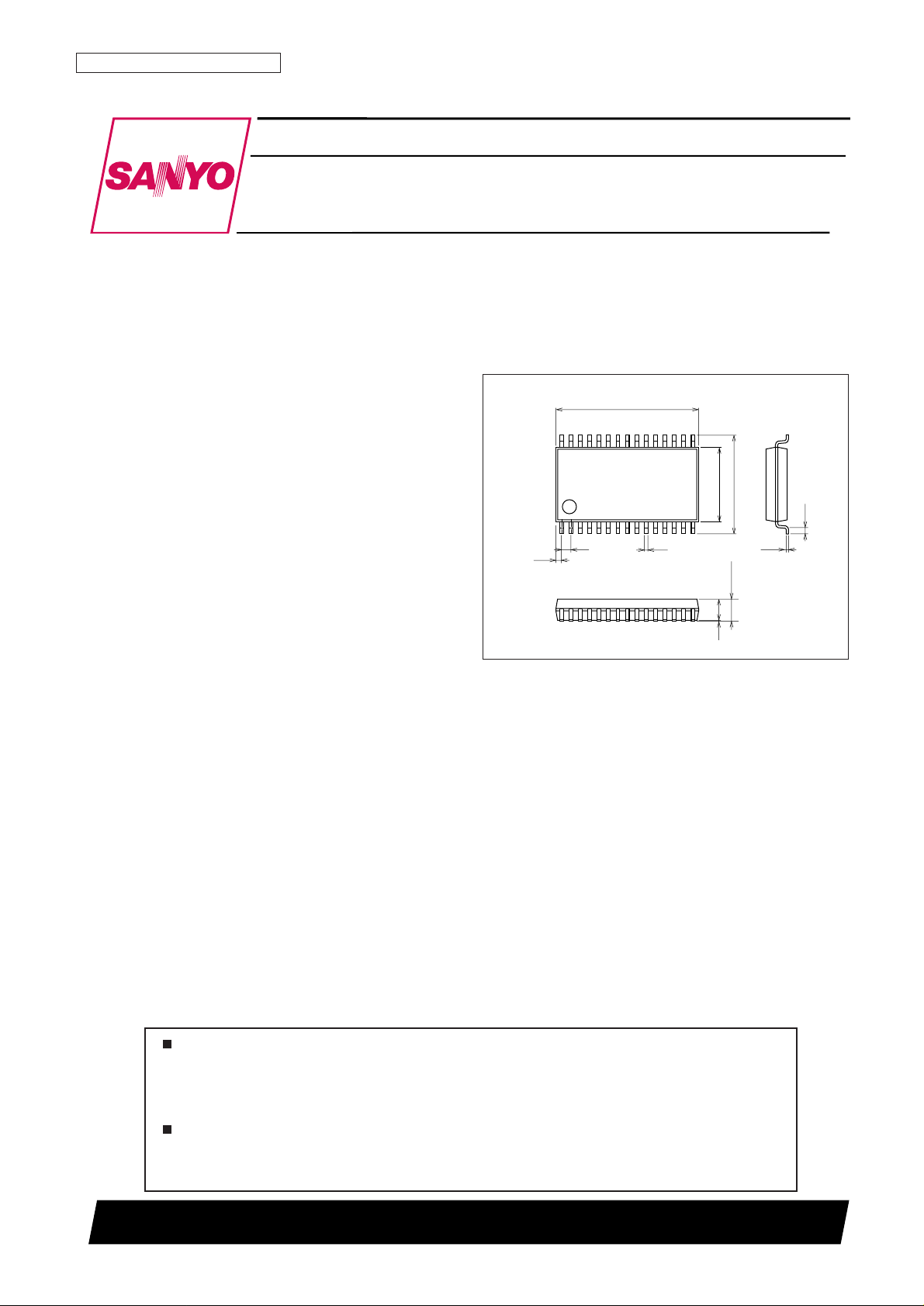
Package Dimensions
unit: mm
3073C-MFP30SD
1
15
30 16
1.0
15.2
0.4
0.65
10.5
7.9
0.25
(0.6)
2.45max
0.1
(2.25)
Preliminary
SANYO: MFP30SD
[LA2351M]
LA2351M
SANYO Electric Co.,Ltd. Semiconductor Company
TOKYO OFFICE Tokyo Bldg., 1-10, 1 Chome, Ueno, Taito-ku, TOKYO, 110-8534 JAPAN
7.5 Mbps Automotive LAN Transceiver
Monolithic Linear IC
Any and all SANYO products described or contained herein do not have specifications that can handle
applications that require extremely high levels of reliability, such as life-support systems, aircraft’s
control systems, or other applications whose failure can be reasonably expected to result in serious
physical and/or material damage. Consult with your SANYO representative nearest you before using
any SANYO products described or contained herein in such applications.
SANYO assumes no responsibility for equipment failures that result from using products at values that
exceed, even momentarily, rated values (such as maximum ratings, operating condition ranges, or other
parameters) listed in products specifications of any and all SANYO products described or contained
herein.
Page 2
No. 6955-2/4
LA2351M
Parameter Symbol Conditions Ratings Unit
Maximum supply voltage V
CC
max With no input signal 7.0 V
Ta ≤ 85°C
Allowable power dissipation Pd max Mounted on a printed circuit board 500 mW
(46.2
× 25.7 × 1.6 mm3, glass epoxy)
Operating temperature Topr –40 to +85 °C
Storage temperature Tstg –55 to +150 °C
Specifications
Maximum Ratings at Ta = 25°C
Parameter Symbol Conditions
Ratings
Unit
min typ max
Recommended supply voltage V
CC
5.0 V
Operating supply voltage range V
CCOP
4.75 5.25 V
D/A converter input
V
ol
Low-level input 0 0.5 V
V
oh
High-level input 2.4 3.3 V
Transmission control input
Vol Low-level input 0.5 V
Voh High-level input 2.4 V
Low-pass filter input amplitude Vlpfi 0.45 0.55 Vpp
Output driver input amplitude Vdrvi 0.45 0.55 Vpp
Receiver amplifier input signal amplitude
Vrxi 15 75 mVpp
range (differential)
Comparator input voltage range Vcpdci 0 3.5 V
Comparator input signal amplitude Vcpi 0.8 1.2 Vpp
Recommended Operating Conditions at Ta = 25°C
Parameter Symbol Conditions
Ratings
Unit
min typ max
Quiescent current Icco When not transmitting 50 70 mA
D/A converter output level Vdao
The deviation with respect to 0.5 V for
–1 0 1 dB
(111) - (001).
Low-pass filter
Output attenuation Vlpfo(9M)
The attenuation of a 9 MHz signal with
2.5 3 3.5 dB
respect to a 1 MHz signal.
Insertion loss Vlpfo(1M) f = 1 MHz –1 0 1 dB
Output driver
Output attenuation Vtxo(15M)
The attenuation of a 15 MHz signal with
0 2 3
respect to a 1MHz signal.
Differential amplification Vtxo(1M) f = 1 MHz –1.5 0 1.5
Receiver amplifier + noise rejection low-pass filter
Amplification Vnfo(1M) f = 1 MHz 25 dB
Frequency characteristics Vnfo(15M)
The Frequency characteristics of a 15 MHz
–3 dB
signal with respect to a 1 MHz signal.
Comparator
Low-level output amplitude Vcpdl 0.2 0.4 0.6 V
High-level output amplitude Vcpdh 3.9 4.2 4.3 V
Operating Characteristics at Ta = 25°C, VCC= 5 V
Page 3

No. 6955-3/4
LA2351M
Pin Functions
Pin No. Pin Function Description Note
1 V
CC
2 Comparator block power supply 5 V
2 CPD2 Comparator inverted output Vol = 0.4 V, Voh = 4.2 V (Maximum voltage: V
CC
2)
3 CPD1 Comparator noninverted output Vol = 0.4 V, Voh = 4.2 V (Maximum voltage: V
CC
2)
4 GND2 Comparator block ground Dedicated ground for the comparator block
5 CP1 Comparator input (+)
6 NFO Noise rejection filter output
7 CP2 Comparator input (-)
8 GND Ground System ground
9 FCC1 Transmission rate setting Low: 5 Mbps, High: 7.5 Mbps
10 BIASC Comparator bias Connect to ground through a capacitor
11 FADJ1
Noise rejection low-pass filter cutoff
Adjusted with a resistor to ground Standard setting: Open
frequency adjustment
12 FADJ2 Low-pass filter cutoff frequency adjustment Adjusted with a resistor to ground Standard setting: Open
13 GCNT Receiver amplifier amplification adjustment
Adjusted with a resistor to ground (capacitor coupled
Standard setting: 0 Ω
ground)
14 RXI2 Reception signal inverting input
15 RXI1 Reception signal noninverting input
16 BIAS2 Bias voltage
17 BIAS1 Bias voltage
18 TXO2 Transmission signal noninverted output
19 TXO1 Transmission signal inverted output
20 NC2 Unused
21 NC1 Unused
22 DRVI Output driver input
23 LPFO Low-pass filter output
24 V
CC
1 Power supply +5.0 V ± 5%
25 /TXEN Transmit/receive switching Low: transmit, High: receive (Vol = 0.5 V, Voh = 2.4 V)
26 LPFI Low-pass filter input
27 DAO D/A converter output 0.5 Vpp ± 1dB
28 TXI2 D/A converter input (MSB) Vol = 0.5 V, Voh = 2.4 V
29 TXI1 D/A converter input Vol = 0.5 V, Voh = 2.4 V
30 TXI0 D/A converter input (LSB) Vol = 0.5 V, Voh = 2.4 V
Page 4

PS No. 6955-4/4
LA2351M
Test Circuit
This catalog provides information as of May, 2001. Specifications and information herein are subject to
change without notice.
Specifications of any and all SANYO products described or contained herein stipulate the performance,
characteristics, and functions of the described products in the independent state, and are not guarantees
of the performance, characteristics, and functions of the described products as mounted in the customer’s
products or equipment. To verify symptoms and states that cannot be evaluated in an independent device,
the customer should always evaluate and test devices mounted in the customer’s products or equipment.
SANYO Electric Co., Ltd. strives to supply high-quality high-reliability products. However, any and all
semiconductor products fail with some probability. It is possible that these probabilistic failures could
give rise to accidents or events that could endanger human lives, that could give rise to smoke or fire,
or that could cause damage to other property. When designing equipment, adopt safety measures so
that these kinds of accidents or events cannot occur. Such measures include but are not limited to protective
circuits and error prevention circuits for safe design, redundant design, and structural design.
In the event that any or all SANYO products (including technical data, services) described or contained
herein are controlled under any of applicable local export control laws and regulations, such products must
not be exported without obtaining the export license from the authorities concerned in accordance with the
above law.
No part of this publication may be reproduced or transmitted in any form or by any means, electronic or
mechanical, including photocopying and recording, or any information storage or retrieval system,
or otherwise, without the prior written permission of SANYO Electric Co., Ltd.
Any and all information described or contained herein are subject to change without notice due to
product/technology improvement, etc. When designing equipment, refer to the “Delivery Specification”
for the SANYO product that you intend to use.
Information (including circuit diagrams and circuit parameters) herein is for example only; it is not
guaranteed for volume production. SANYO believes information herein is accurate and reliable, but
no guarantees are made or implied regarding its use or any infringements of intellectual property rights
or other rights of third parties.
V
CC
DATA OUT
TXI0
DAC
TXI1 TXI2
RADO
0.1µ
TXEN
V
V
CC
0.1µ
CC
3.3µ
0.1µ
0.1µ
30 29 28 27 26 25 24 23 22 21 20 19 18 17 16
DAC
Comparater
LPF
Driver Amp
Receiver Amp
Noise
Filter
1 2 3 4 5 6 7 8 9 10 11 12 13 14 15
3.3µ
0.1µ
0.1µ
OUTPUT
V
CC
3.3 V
COMP.
GND
0.1µ
33k
GND CUT_OFF
CONTRO
0.1µ
COMP
BIAS
0.1µ
0.1µ
0.1µ
0.1µ
2.2k
2.2k
V
CC
0.1µ
5.6k
330
330
5.6k
0.1µ
 Loading...